Flexoelectric electricity generation by crumpling graphene
←
→
Page content transcription
If your browser does not render page correctly, please read the page content below
Flexoelectric electricity generation by
crumpling graphene
Cite as: J. Appl. Phys. 129, 225107 (2021); https://doi.org/10.1063/5.0052482
Submitted: 31 March 2021 . Accepted: 19 May 2021 . Published Online: 14 June 2021

  Brahmanandam Javvaji,        Ranran Zhang,       Xiaoying Zhuang, and Harold S. Park

J. Appl. Phys. 129, 225107 (2021); https://doi.org/10.1063/5.0052482                     129, 225107

© 2021 Author(s).
Journal of                                                                                         ARTICLE            scitation.org/journal/jap
 Applied Physics

    Flexoelectric electricity generation by crumpling
    graphene
    Cite as: J. Appl. Phys. 129, 225107 (2021); doi: 10.1063/5.0052482
    Submitted: 31 March 2021 · Accepted: 19 May 2021 ·                                                                    View Online   Export Citation     CrossMark
    Published Online: 14 June 2021

    Brahmanandam Javvaji,1                    Ranran Zhang,1      Xiaoying Zhuang,1,2,a)        and Harold S. Park3

    AFFILIATIONS
    1
     Computational Science and Simulation Technology, Institute of Photonics, Faculty of Mathematics and Physics,
    Leibniz Universität Hannover, Appelstr. 11A, 30167 Hannover, Germany
    2
        Department of Geotechnical Engineering, College of Civil Engineering, Tongji University, 1239 Shanghai 200092, China
    3
        Department of Mechanical Engineering, Boston University, Boston, Massachusetts 02215, USA

    Note: This paper is part of the Special Topic on Trends in Flexoelectricity.
    a)
        Author to whom correspondence should be addressed: zhuang@iop.uni-hannover.de

    ABSTRACT
    We utilize atomistic simulations that account for point charges and dipoles to demonstrate that flexoelectricity, which arises from strain
    gradients, can be exploited to generate electricity from crumpled graphene sheets. Indentation of a circular graphene sheet generates
    localized developable (d)-cones, for which we verify the core radius and azimuthal angle with established theoretical models. We determine
    the voltage that can be generated based on the resulting electrostatic fields and compare the voltage generation to previous theoretical
    predictions that are scaled down to the nanoscale. In doing so, we find that the voltage generated from crumpling graphene exceeds, by
    about an order of magnitude, the expected voltage generation, indicating the benefit of exploiting the large strain gradients that are possible
    at the nanoscale. Finally, we demonstrate that crumpling may be a superior mechanism of flexoelectric energy generation as compared to
    bending of two-dimensional nanomaterials.

    Published under an exclusive license by AIP Publishing. https://doi.org/10.1063/5.0052482

    I. INTRODUCTION                                                             bonded electrons (π  σ interactions).32 This change in bonding due
                                                                                to strain gradients from bending leads to the generation of electrical
          Two-dimensional (2D) nanomaterials have been widely studied
    because of their novel physical properties.1–11 An emerging applica-        polarization via local electric fields and thus the emergence of flexoe-
                                                                                lectricity.12 Flexoelectricity has also been reported in other 2D mate-
    tion area for 2D materials is that of electromechanical energy
                                                                                rials.17 For example, the monolayer transition metal dichalcogenides
    generation12–18 due to their potential for nanoscale energy harvesting
                                                                                (TMDCs) exhibit a flexoelectric response that is one order of magni-
    and generation.19,20 In this vein, piezoelectricity, the best-known
                                                                                tude higher than graphene.12 Furthermore, Janus TMDCs show
    mechanism for converting mechanical deformation into electrical             exceptional bending flexoelectric properties related to the initial
    energy, has been studied in 2D materials.21–23 In contrast, flexoelec-      degree of asymmetry13 and exhibit flexoelectric constants that exceed
    tricity, for which the polarization of the material depends upon the        graphene and TMDCs. The flexoelectric properties of other recently
    strain gradient, has been less studied as an energy generation and          synthesized monolayers have also been investigated.16,33,34 These
    conversion mechanism for 2D materials.23–29 Because flexoelectricity        recent studies have demonstrated the promising potential of 2D
    depends on the strain gradient, it is, unlike piezoelectricity, theoreti-   materials for flexoelectric energy generation and conversion.
    cally possible in any material and has been recently studied in 2D                Here, we investigate the potential for generating electricity by
    materials.                                                                  crumpling 2D materials, specifically graphene. This work is moti-
          Graphene is a centrosymmetric material that does not exhibit          vated by recent experimental studies on electrical power generation
    piezoelectricity.30,31 However, bending graphene can induce a change        by crumpling thin polymer films35 and theoretical works on flexo-
    in hybridization from sp2 to sp3 , where the valence electrons of the       electric energy generation by crumpling thin sheets, such as paper,36
    carbon atoms develop bonding interactions with the neighboring              in which electricity was produced via the flexoelectric effect by

J. Appl. Phys. 129, 225107 (2021); doi: 10.1063/5.0052482                                                                                                 129, 225107-1
Published under an exclusive license by AIP Publishing
Journal of ARTICLE scitation.org/journal/jap
Applied Physics
crumpling thin circular sheets supported on a hoop via central works.12,31 All the simulations in this work were conducted using
forces created by a cone tip. Of specific interest is the formation of a the open-source MD code LAMMPS.40 The visual molecular
developable (d)-cone during the indentation, as the simplest example dynamics (VMD) package41 has been used to generate the atomic
of thin sheet crumpling, which generates strain gradients and thus snapshots.
the development of electrical polarization and voltage. Here, we The interactions between the CGS and both CNTs (the inden-
examine the potential of crumpling atomically thin sheets, specifically tor and hooper) were limited to van der Waals forces to avoid
monolayer graphene, as a means of electromechanical energy genera- bonded interactions between the CGS and CNTs, where the van der
tion at the nanoscale. We do this via classical molecular dynamic Waals forces were modeled using a Lennard–Jones potential.42 In
simulations that account for point charges and dipoles to investigate the initial simulation setup, db and dt are set as 0.33 nm at which the
the mechanisms driving the voltage generated from the indentation, CGS and the CNTs have minimum potential energy and thus no
and subsequent crumpling, of a monolayer graphene sheet. interaction forces. Both the CNT hooper and CNT indenter are
modeled as rigid bodies, while the CGS is allowed to slide, via the
van der Waals forces, over the CNT hooper in response to the CNT
II. SIMULATION METHOD indentor. The CNT hooper is fixed spatially throughout the indenta-
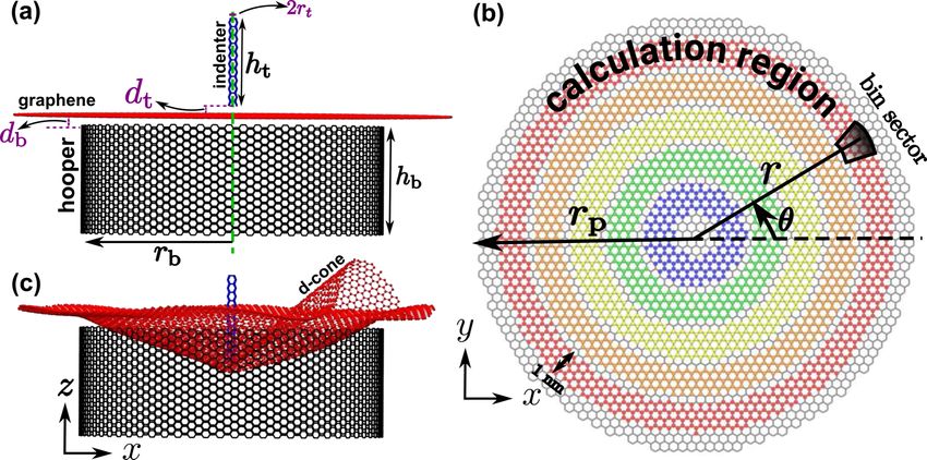
Figure 1(a) shows the simulation setup used to conduct the tion process.
atomistic simulations. We consider a circular graphene sheet (CGS) The CGS was initially equilibrated using the Nosé–Hoover
of radius r p placed on top of a carbon nanotube (CNT) of radius rb thermostat43,44 for about 100 000 steps with a time step of 0.5 fs at
with height hb at a distance of db . This CNT acts as a supporting a temperature of 0.1 K to minimize thermal fluctuations. The
hoop (called the hooper) for the CGS. Another CNT, which is used indenter CNT moves with a speed of 0.02 nm/ps toward the CGS,
to indent the CGS, with radius rt and height ht , is initially located where the atomic positions are integrated forward in time using a
at a distance dt from the CGS. The interatomic forces acting on standard velocity Verlet algorithm.45 The atomic coordinates along
each atom in the CGS were calculated using a combination of with the charge and dipole data are collected at every 1000
short-range bonded interactions and long-ranged charge–dipole steps during the time integration. We vary the CGS radius (r p )
(CD) interactions. The AIREBO potential37 was employed to from 7 to 10 nm to study the effect of the graphene sheet size
account for the short-range bonded interactions, while for the CD during the crumpling deformation and the resultant voltage gener-
interactions, each atom is assumed to carry a charge q and dipole ation. However, we varied the radius of both the indentor and
moment p.38,39 The minimization of charge–charge, charge–dipole, hooper CNTs to ensure the same percentage of the CGS is
and dipole–dipole interactions to the total system energy leads to indented, regardless of CGS diameter. About 25% of CGS atoms
the governing equations for obtaining the charge and dipole are supported by the hooper and 0.025% of CGS atoms are
moments for each atom. The complete details about the implemen- indented by the top CNT. The 100-fold reduction in the indented
tation of the CD model in conjunction with a classical molecular atoms as compared to the supported atoms is to mimic a sharp
dynamics (MD) simulation can be found in our previous indenter tip.
FIG. 1. (a) Schematic of the circular graphene sheet supported on CNT for deformation by indentation. (b) In-plane view of the setup in (a). Region used for calculation
highlighted with red color. Within this region, several bin sectors were constructed to evaluate physical quantities of interest. (c) represents the d-cone formation under
indentation.
J. Appl. Phys. 129, 225107 (2021); doi: 10.1063/5.0052482 129, 225107-2
Published under an exclusive license by AIP Publishing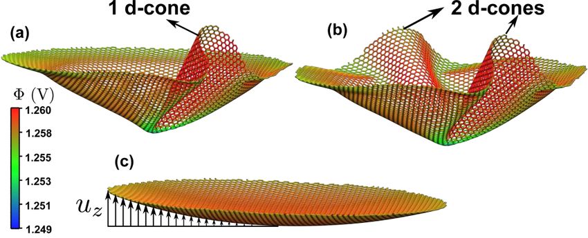
Journal of ARTICLE scitation.org/journal/jap
Applied Physics
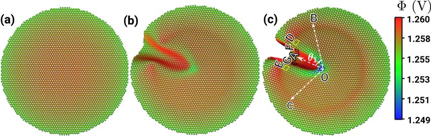
FIG. 2. Atomic snapshots of the 9 nm CGS when the indentation depth is (a) 0, (b) 1.546, and (c) 2.541 nm. Atoms in (a)–(c) are colored using the electrostatic potential
Φ for 9 nm CGS. Note the development of the d-cone in (b) and (c). Labels!
O, A, B, and C represent the CGS center or d-cone core, the d-cone tip, and the edges of the
d-cone, respectively. D,
! E, F, and G denote
! the!atom bins nearer to bin A. OA represents the bin sector with the largest z deflection and for this bin, we set θ as 0 . θ 1
is the angle between OA and either OB or OC .
We define several circular regions starting from the center of The initial thermally equilibrated atomic configuration of the CGS
the CGS. These regions have a width of about 1 nm and radius r in Fig. 2(a) shows small out-of-plane fluctuations near the edges, as
varying from 1 to r p -2 nm, as shown in Fig. 1(b). Furthermore, expected as the edges are not fixed. The low system temperature of
each region is subdivided into 60 bin sectors as highlighted in 0.1 K suppresses large edge fluctuations or ripples, which have an
Fig. 1(b). For these sectors, we averaged the atomic coordinates, amplitude of 0.1 nm in the z-(out of plane) direction. The indenta-
potential energy, voltage, charges, and dipole moments at a series tion induces deformation at the center of the CGS, which through
of indentation steps. The local curvature κ of the bin sector is esti- bond bending and stretching extends to deform the rest of the
mated from the derivatives of spline interpolations with respect to CGS. Figure 2(b) clearly indicates a non-uniform change of
the averaged x and y coordinates of each bin. At each indentation out-of-plane displacements in a confined portion of CGS. Further
step, we consider the atoms with minimum z- coordinates near to indentation increases the deformation and the atomic configuration
the core portion of the developable (d)-cone to define the center of in Fig. 2(c) clearly shows the formation of a developable cone
the CGS, which is labeled “O” in Fig. 2(c). Those atoms are used (d-cone) due to crumpling.
for measuring the depth and inner voltage ΦO . The tip deflection is The deformation in the graphene sheet changes the local elec-
the difference between the initial and indented z-coordinates for trostatic fields and thus induces polarization by altering the charges
atoms associated with O. Figure 1(c) represents the d-cone forma- and dipole moments through piezoelectricity and flexoelectricity.
tion due to the indentation of CGS. However, due to the absence of piezoelectricity in graphene, the
We define two dimensionless parameters to aid in the analysis. only electrical response we can measure is due to flexoelectricity.
The dimensionless parameter α1 is the ratio between depth and rb , The governing equation for the charges q and dipoles p in the
which can be interpreted as the dimensionless tip deflection. charge–dipole model is12
Another dimensionless parameter α2 ¼ Rc =rb , where Rc is the core
radius, and so α2 can be interpreted as the dimensionless core qq
X
N
qq
X
N
qp
radius. Using these two parameters, we further compare our simu- Tii qi þ Tij qj Tij pj ¼ χ i : (1)
lation results with the earlier reported models,36 which were per- j,i=j j,i=j
formed at significantly larger length scales. Finally, we note that the
electromechanical energy density is defined as the sum of the dot From Eq. (1), the electrostatic potential Φ associated with each
product between the polarization and the electric fields over the atom is written as
CGS area, while the strain energy density is the scalar valued tensor
qq p q
product of atomic stress and atomic strain over the same area of Φi ¼ Tii qi ¼ Φi þ Φi þ χ i , (2)
the CGS. The electromechanical energy density is equal to the elec- P
q qq
trical energy density stored in an energy harvester when subjected where Φi ¼ Nj,i=j Tij qj is the electrostatic
P potential on atom i
p qp
only to mechanical loads.46–48 due to the neighboring charges qj , Φi ¼ Nj,i=j Tij pj is the elec-
trostatic potential on atom i due to the neighboring dipoles pj ,
qq
III. RESULTS AND DISCUSSION Tii is the self-electrostatic potential for atom i to create a charge
qi , and χ i is the electron affinity of atom i. Equation (2) refers to
A. Verification of crumpling simulations the generation of electric charge qi due to the various electrostatic
We first demonstrate that our atomistic simulations of potentials Φi associated with atom i. From Eq. (2), we can calculate
graphene crumpling follow previous theoretical results.36,49,50 the electrostatic potential associated with each atom. By noting the
J. Appl. Phys. 129, 225107 (2021); doi: 10.1063/5.0052482 129, 225107-3
Published under an exclusive license by AIP Publishing
Journal of                                                                                                            ARTICLE               scitation.org/journal/jap
 Applied Physics

    time-history of Φ for every atom, we can estimate the voltage gen-                         CGS curvature κ with θ is shown in Fig. 3(a). κ is nearly constant
    erated due to the crumpling deformation.                                                   for bins with small out-of-plane displacements, which occur for
          Figures 2(a)–2(c) show the atomic configuration colored using                        bins away from the d-cone. However, κ changes rapidly near the
    Φ estimated from Eq. (2). In Fig. 2(a), initially, the inner atoms                         region where the d-cone forms. For r p =8 nm, κ shows an increase
    have Φ ¼ 1:258 V and outer edge atoms have Φ ¼ 1:255 V. The                                from 63 to 30 [corresponding atom bins are marked as B and
    atoms near the boundary exhibit lower electrostatic fields than the                        D in Fig. 2(c) and in the inset of Fig. 4(a)]. The positive rise of κ
    central atoms. The structural changes due to indentation alter the                         between B to D corresponds to the left portion of the d-cone,
    local electric fields near the central portion of CGS, which results                       where the out-of-plane (z) deflections increase rapidly. From there
    in highly localized changes in Φ (about 4 mV reduction) from                               κ decreases with increasing out-of-plane deflection and reaches a
    Figs. 2(a) to 2(b) due to the flexoelectric effect. Specifically, the ini-                 negative maxima at 0 , labeled as A, which corresponds to the
    tiation of the d-cone formation and increased bending in Fig. 2(b)                         d-cone region with the largest out-of-plane displacements [the
    leads to a change of hybridization (pyramidalization) from sp2 to                          central line of the d-cone O-A in Fig. 2(c)]. As θ increases, an
    sp3 for the atoms near the center, leading to a change in the bond                         effectively symmetric response of κ is observed, with similar
    angle from 120 to 117 with a 3% stretch in the bond lengths.                             responses seen for CGS with radius 7, 9, and 10 nm.
    These changes in the bond length and bond angles induce the                                      Note that the choice of the calculation region radius r is 4 nm,
    observed inhomogeneity in Φ that extends across the d-cone.                                which keeps the distance of separation between the bins O and A
          In Fig. 2(c), the core portion of the d-cone (labeled as O)                          the same across the different sized CGS, while all atomic configura-
    shows a decrease of Φ from 1.258 to 1.249 V of about 9 mV when                             tions were analyzed at α1 ¼ 0:545 to enable a consistent comparison
    compared to Fig. 2(a), where label A indicates the bin sector with                         for different CGS sizes. Importantly, we find that θ1 is about 62 for
    maximal outward deflection, where Φ rises 2 mV from 1.257 to                               all CGS we considered, which matches earlier theoretical and experi-
              !
    1.259 V. OA represents the connecting line between bins O and A,                           mental results where θ1 ranged from about 60 49 to 70 .50
    which is used to define θ to identify the relative positions of the                              To further validate our simulations, we explore the response
                                                            !
    other neighboring bins, as θ ¼ 0 corresponds to OA . From this                             to indentation as a function of the dimensionless tip deflection α1 .
    line, the atomic deformation as well as changes in Φ extends to the                        The core radius Rc is estimated from the locations of the bin
                                                                     !
    bins labeled as B and C, where the region between lines OB and                             sectors corresponding to the d-cone. The inset of Fig. 3(b) illus-
    !                                                               !
    OC covers the d-cone involved crumpled area. Near line OA , the                            trates selected bins as red color dots. Note that we consider only
    strain gradient-induced changes in the potential are clearly visible                       the x and y coordinates for these bins. We then established a
    with respect to the d-cone folding [in Figs. 2(b) and 2(c)].                               hyperbolic fitting51 across the coordinate set [shown as a blue line
    However, outside of this region, there are only small changes in                           in the inset of Fig. 3(b)], where Rc is the inverse curvature at the
    potential due to the relatively small deformations of the graphene                         vertex of the fitted hyperbola. This process is repeated for the
    atoms in response to the indentation.                                                      entire time-history of atomic configurations and all CGS systems.
          This is further verified by plotting the local curvature κ and Φ                     The variation of α2 is nearly constant for α1 less than 0.243
                                                         !
    across the different bin sectors defined from line OA . The resulting                      [Fig. 4(a)], which means that the indentation does not yield a

      FIG. 3. (a) The variation of curvature κ with bin angle θ for different r p when α1 ¼ 0:545, where the calculation region radius is 4 nm from O. (b) The variation of (a) α2
      or Rc with α1 when r p varies from 7 to 10 nm. The inset in (b) indicates the scheme for calculating core radius Rc . The blue line represents the fitting hyperbola.

J. Appl. Phys. 129, 225107 (2021); doi: 10.1063/5.0052482                                                                                                                 129, 225107-4
Published under an exclusive license by AIP Publishing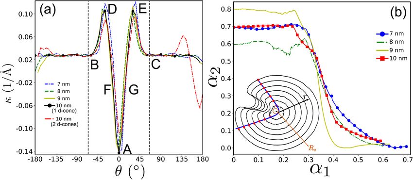
Journal of                                                                                                           ARTICLE               scitation.org/journal/jap
 Applied Physics

    significant deflection near the outer edges of the CGS. The initiation                    difference. For example, consider the CGS with r p ¼ 9 nm at
    of out-of-plane z deflection leads to a decrease in the distance of sep-                  α1 ¼ 0:462, where the total in-plane electric fields (Ex and Ey ) are
    aration between hyperbolic asymptotes, which leads to a decrease in                       about 30 times smaller than the out-of-plane electric field (Ez ). In
    the core radius. When α1 is above 0:25, α2 or Rc shows a decreasing                       total, the developed π  σ interactions increase the local electric
    trend in Fig. 3(b), which matches observed trends previously                              fields and thus the potential Φ for the associated atoms.
    obtained for thin films.36 These observations (Fig. 3) suggest that                             Between regions F and A, a 1.7 mV drop in the potential dif-
    our MD simulation results for monolayer graphene match previous                           ference is observed. In this region, the large deformations increased
    studies on d-cone formation in crumpled thin sheets.                                      the bond length by 0:614% and decreased the bond angle by
                                                                                              0:488%. The increase in the bond length again reduces the local
                                                                                              electric fields and decreases the voltage in this region as shown in
    B. Flexoelectric voltage generation                                                       Fig. 4(a). Because the deformation of the d-cone is symmetric
                                                                                                      !
          Figure 4(a) shows the bin averaged potential difference                             about OA , the changes in potential going from A to G and G to E
    Φ  ΦO with respect to θ when α1 ¼ 0:545 and where the calcula-                           are similar to those previously discussed in going from D to F and
    tion region radius is 4 nm from O. For the 8 and 9 nm CGS, the                            F to A.
    potential difference is constant for regions outside of the d-cone                              For the 7 nm CGS, in addition to the above observations, the
    due to the small deformations there. From bins represented by                             atoms in the calculation region are impacted by edge atom effects,
    labels B to D, there is a decrease in Φ  ΦO of about 1 mV. In this                       which cause an increase and then a decay in the developed poten-
    region, the bond angle decreases by 0:110%, while the bond length                         tial difference from the d-cone edges to the other portion of the
    increases by 0:363%. This increase in bond separation decreases the                       CGS. Overall, the variation of Φ  ΦO is significant within
    local electric fields, thus reducing the generated potential.                             θ  jθ1 j, which again indicates that the largest potential differences
          From region D to F, Φ  ΦO reaches 12.336 mV, despite the                           are confined to regions near the d-cone in Fig. 2(c). A zoom over
    average change in the bond length being only 0:033% and the                               one side of the d-cone [the inset of Fig. 4(a)] visualizes the voltage
    average change in angle being only 0:115%. Thus, the large poten-                         for bins A, B, D, and F more clearly.
    tial difference is driven by pyramidalization,52–54 in which                                    For the 10 nm CGS, we found that the number of d-cones that
    increased interactions between π and σ electrons take place due to                        a form exhibits some sensitivity to the initial conditions. For the
    increased curvature. Specifically, the changes in curvature tilt the σ                    10 nm CGS with a single d-cone (marked as 1 d-cone), Fig. 4(a)
    bonds and break the symmetry in the π orbitals, which induces an                          shows that it exhibits similar behavior to the smaller CGS consid-
    electron transfer and creates local electric fields. The bond tilt                        ered. However, the 10 nm CGS with multiple d-cones exhibits dif-
    changes the pyramidalization angle between the σ bonds to the π                           ferent behavior, which we now discuss. Specifically, for the 10 nm
    orbital axis vector, which is a function of bond angles between σ                         CGS with two d-cones, Fig. 4(a) (labeled as 2 d-cones) shows a
    bonds.55 The large in-plane electrical conductivity screens most of                       2 mV reduction in Φ  ΦO between bins B to C, which is smaller
    the generated in-plane electric fields, whereas there exist the                           than for the smaller radii CGS. In addition, we note there is a
    out-of-plane electric fields that involve the generation of voltage                       second rise in the potential difference starting from θ . 113 ,

      FIG. 4. (a) The variation of voltage Φ  ΦO with bin angle θ for different r p when α1 ¼ 0:545, where the calculation region radius is 4 nm from O. The inset in (a) indi-
      cates one side of the d-cone. Atomic coloring follows the color scale bar in Fig. 2. (b) The variation of ΦA  ΦO with α1 when r p varies from 7 to 10 nm. The inset in (b)
      represents the variation of Φ with α1 for 9 nm CGS.

J. Appl. Phys. 129, 225107 (2021); doi: 10.1063/5.0052482                                                                                                                129, 225107-5
Published under an exclusive license by AIP Publishing
Journal of                                                                                                   ARTICLE            scitation.org/journal/jap
 Applied Physics

    which represents the generation of a secondary d-cone for the                               Figure 4(b) shows the variation of potential difference ΦA  ΦO
    10 nm CGS. The associated curvature changes in Fig. 3(a) (labeled                     with respect to α1 . Here, we considered only the response of bin A,
    as 2 d-cones) further supports this observation. The rise of the                      which contains the maximum deflections due to the d-cone, for
    second d-cone further reduces the deformation near to the central                     studying the response with α1 . For α1 less than 0.1, there is no differ-
    portion of the CGS, which makes the average potential for O for the                   ence in the electrostatic potential between bins A and O. For α1
    10 nm CGS to be 1.251 V whereas it is 1.248 V for the other CGS at                    between 0.1 and 0.3, as shown in the inset of Fig. 4(b), there is no
    the same α1 . As a result, the total Φ  ΦO is smaller for the 10 nm                  observable change in potential for bin A. However, because the
    CGS with two d-cones as compared to the other CGS we considered.                      indenter deforms and stretches the atoms near the CGS center,
    Figures 5(a) and 5(b) visualizes the atomic configurations for 10 nm                  this results in a decrease of ΦO , leading to an increase in potential
    CGS with the development of one and two d-cones. For the 10 nm                        difference ΦA  ΦO . Starting at α1 ¼ 0:3, ΦA begins increasing
    CGS with two d-cones, the atoms associated with the secondary                         due to the formation of the d-cone. While the edges of the d-cone
    d-cone experienced enhanced charges, dipoles, and electrostatic                       (bins B and C) show no changes in potential, this indicates the locali-
    fields, which can be viewed as enhanced Φ for the atoms in the two                    zation of deformation near the d-cone seen in Fig. 2(c). Further
    d-cones in Fig. 5(b) when compared to Fig. 5(a). This is quantified                   indentation leads to larger potential differences ΦA  ΦO , though the
    using the comparison of energy densities between 9 and 10 nm CGS.                     rate of potential increase decreases. These trends are observed for all
    For the 10 nm CGS with two d-cones at α1 ¼ 0:545, the strain                          CGS we simulated.
    energy density is 1:341  106 J=m2 and the electrical energy                               The observed voltage variation shows a similar trend with
    density is 9:927  106 J=m2 . At nearly the same strain energy                       earlier theoretical predictions.36 We note that the potential differ-
    density, the 9 nm CGS yields 4:871  106 J=m2 as the electrical                      ence from our simulations on monolayer graphene is about 100
    energy density, which is 32% smaller than that in 10 nm case, which                   times smaller than the generated flexoelectric part of voltage from a
    indicates the importance of the secondary d-cone. Although the                        poly vinyldenefluoride (PVDF) thin film. Thus, even though the
    average potential for the 10 nm CGS is lower compared to the 9 nm                     flexoelectric constant for graphene (0:003 nC/m12) is about 1000
    CGS, the increase of contribution from the secondary d-cone atoms                     times smaller than PVDF (13 nC/m20), there is a 10 fold increase
    increase the total electrical energy density.                                         in the generation of voltage for crumpled graphene as compared to
          To understand why the voltage Φ  ΦO from the 10 nm CGS                         the scaled analytic theory. There are at least two important implica-
    is smaller than the 9 nm CGS despite the generation of more elec-                     tions of this. First, this is likely due to the larger strain gradients
    trical energy density due to the two d-cones, we consider atomic                      that are possible at the nanoscale for a comparable deformation
    insights from bond stretching and changes in the bond angle. The                      mode (d-cone based crumpling), which implies benefits of
    average change in the bond length and bond angle for atoms                            crumpling-based electromechanical energy conversion at the nano-
    between bins O and A for atomic configuration with α1 ¼ 0:545 is                      scale. Furthermore, nanoscale systems can sustain such large strain
    0.074 Å and 0:438 , respectively, for the 10 nm CGS with two                         gradients without creating atomic defects or cracks, which is benefi-
    d-cones. For the 10 nm CGS with one d-cone, we find the average                       cial for longer duration stability and durability. Finally, because
    change in the bond length as 0.113 Å and the bond angle as 0:673 .                   other 2D materials such as the TMDCs have both a significantly
    For the 9 nm CGS at the same α1 , these changes are 0.113 Å and                       larger flexoelectric constants and non-zero piezoelectric response as
    0:718 . The smaller changes in the atomic configuration for 10 nm                    compared to graphene,12,13 there may be additional enhancements in
    CGS with two d-cones results in smaller strain gradients, and thus                    nanoscale flexoelectric energy generation through optimal material
    the resulting potential difference is lower as compared to the 10 nm                  choices. Introducing the dopant mediated asymmetry in a composite
    CGS with one d-cone and the 9 nm CGS.                                                 material56,57 may further help one to improve the flexoelectric effect
                                                                                          under crumpling deformation.

                                                                                          C. Benefits of crumpling for nanoscale flexoelectric
                                                                                          energy generation
                                                                                                Finally, we discuss the potential benefits of crumpling gra-
                                                                                          phene for nanoscale flexoelectric energy generation by comparing
                                                                                          the response to the standard mode of flexoelectric energy genera-
                                                                                          tion, that of pure bending. To do so, we impose a displacement
                                                                                          field uz ¼ 12 K(x2 þ y2 ) to the atoms in the CGS, where K repre-
                                                                                          sents the strain gradient, and x and y represent the atom coordi-
                                                                                          nates in the x and y directions. In these simulations, only the CGS
                                                                                          is considered, i.e., there is no CNT indenter or hooper. A circular
                                                                                          region of atoms with a radius greater than r p -0.5 nm was selected
      FIG. 5. Atomic snapshots of the indented CGS of radius 10 nm with (a) one           as the boundary atoms for the given CGS with radius r p ; these
      d-cone (label 1 d-cone) and (b) two d-cones (label 2 d-cones). (c) Atomic view      boundary atoms are fixed whereas all other atoms are allowed to
      of 9 nm CGS under bending deformation. The radial increment of displacement         relax due to the prescribed deformation for 1000 time steps under
      field uz represent the applied bending deformation. The visualized atomic config-
      urations collected at the same strain energy density of 1:341  106 J=m2 .
                                                                                          thermostat condition, the point charges and dipole moments are
                                                                                          found for each atom using the charge–dipole model, after which

J. Appl. Phys. 129, 225107 (2021); doi: 10.1063/5.0052482                                                                                                 129, 225107-6
Published under an exclusive license by AIP Publishing
Journal of ARTICLE scitation.org/journal/jap
Applied Physics
the local electric field and electrostatic potentials are also deter- effect. Finally, we anticipate that other 2D materials, such as the
mined. Figure 5(c) shows the graphene atomic configuration under TMDCs, will exhibit superior flexoelectric energy generation under
bending deformation. crumpling as compared to graphene; we plan to present such com-
Using this information, we compared the electrical energy parisons in future work.
density for atomic configurations at the same strain energy density
for a 9 nm radius CGS deformed using crumpling and bending, fol- ACKNOWLEDGMENTS
lowing the bending methodology described in our previous works12,31
as well as in recent experiments.25 During the calculation of energy X. Zhuang would like to acknowledge the ERC Starting Grant
densities, we note that only the non-fixed interior atoms are used and (No. 802205) and NSFC (No. 11772234).
the number of atoms is the same for both crumpling and bending
simulations. The atomic configuration under crumpling deformation DATA AVAILABILITY
at α1 ¼ 0:545 gives an electrical energy density of 4:871 106 J=m2
The data that support the findings of this study are available
and a strain energy density of 1:341 106 J=m2 . Selecting an
from the corresponding authors upon reasonable request.
atomic configuration for bending deformation of the 9 nm CGS with
nearly the same strain energy density (1:381 106 J=m2 ) results in
an electrical energy density 1:5 106 J=m2 , which is about 70% REFERENCES
lower than for crumpling. 1
E. Pop, V. Varshney, and A. K. Roy, “Thermal properties of graphene:
The main difference between crumpling and bending is Fundamentals and applications,” MRS Bull. 37(12), 1273–1281 (2012).
2
related to the strain gradients. For bending, the displacement field S. Ghosh, W. Bao, D. L. Nika, S. Subrina, E. P. Pokatilov, C. N. Lau, and
uz is symmetric about the center of the CGS, which results in a A. A. Balandin, “Dimensional crossover of thermal transport in few-layer gra-
uniform strain gradient, and thus lower electric fields, charges and phene,” Nat. Mater. 9(7), 555 (2010).
dipole moments due to flexoelectricity. In crumpling, the out of
3
R. Fei and L. Yang, “Strain-engineering the anisotropic electrical conductance
of few-layer black phosphorus,” Nano Lett. 14(5), 2884–2889 (2014).
plane deformation uz is non-uniform about the CGS, and eventu- 4
S. Yu, X. Wu, Y. Wang, X. Guo, and L. Tong, “2D materials for optical modula-
ally results in the formation of a localized d-cone, which exhibits
tion: Challenges and opportunities,” Adv. Mater. 29(14), 1606128 (2017).
significant and non-uniform strain gradients, resulting in enhanced 5
Q. H. Wang, K. Kalantar-Zadeh, A. Kis, J. N. Coleman, and M. S. Strano,
local electric fields and flexoelectric response yielding larger voltage “Electronics and optoelectronics of two-dimensional transition metal dichalcoge-
generation. To quantify this, we first note that the voltage difference nides,” Nat. Nanotechnol. 7(11), 699 (2012).
between bins A and O (ΦA ΦO ) in the bending case is 0.566 mV, 6
P. Z. Hanakata, A. Carvalho, D. K. Campbell, and H. S. Park, “Polarization and
while it is 10.641 mV for crumpling. The average change in the valley switching in monolayer group-IV monochalcogenides,” Phys. Rev. B
bond length (0.009 Å) and the bond angle (0:336 ) in bending are 94(3), 035304 (2016).
also lower compared to crumpling. We also calculated the potential
7
R. C. Andrew, R. E. Mapasha, A. M. Ukpong, and N. Chetty, “Mechanical
difference ΦR ΦO , where ΦR represents the average potential for properties of graphene and boronitrene,” Phys. Rev. B 85(12), 125428 (2012).
8
B. Javvaji, P. Budarapu, V. Sutrakar, D. R. Mahapatra, M. Paggi, G. Zi, and
all atoms besides the boundary atoms and those in bin O. This dif-
T. Rabczuk, “Mechanical properties of graphene: Molecular dynamics simula-
ference is 1.52 mV for bending and 8.41 mV for crumpling, again tions correlated to continuum based scaling laws,” Comput. Mater. Sci. 125,
demonstrating the significant increase in flexoelectric energy gener- 319–327 (2016).
ation for crumpling compared to bending. Overall, this shows that 9
S. J. Kim, K. Choi, B. Lee, Y. Kim, and B. H. Hong, “Materials for flexible,
the uniform strain gradient from bending results in less localized stretchable electronics: Graphene and 2D materials,” Annu. Rev. Mater. Res. 45,
deformation, strain gradients, and thus generated flexoelectric 63–84 (2015).
voltage than crumpling. 10
Z. Sun, A. Martinez, and F. Wang, “Optical modulators with 2D layered mate-
rials,” Nat. Photonics 10(4), 227 (2016).
11
R. Mas-Ballesté, C. Gómez-Navarro, J. Gómez-Herrero, and F. Zamora, “2D
IV. CONCLUSION materials: To graphene and beyond,” Nanoscale 3(1), 20–30 (2011).
12
X. Zhuang, B. He, B. Javvaji, and H. S. Park, “Intrinsic bending flexoelectric
We utilized classical molecular dynamics coupled with the constants in two-dimensional materials,” Phys. Rev. B 99(5), 054105 (2019).
charge–dipole model to investigate the potential of flexoelectric 13
B. Javvaji, B. He, X. Zhuang, and H. S. Park, “High flexoelectric constants in
energy generation in graphene, the model 2D nanomaterial, due to Janus transition-metal dichalcogenides,” Phys. Rev. Mater. 3(12), 125402 (2019).
crumpling deformations. After verifying that our simulations quali- 14
L. J. McGilly, A. Kerelsky, N. R. Finney, K. Shapovalov, E.-M. Shih,
tatively reproduced previous predictions for d-cone characteristics, A. Ghiotto, Y. Zeng, S. L. Moore, W. Wu, Y. Bai, K. Watanabe, T. Taniguchi,
including core radius and non-dimensional indentation depth, we M. Stengel, L. Zhou, J. Hone, X. Zhu, D. N. Basov, C. Dean, C. E. Dreyer, and
examined the mechanisms controlling the flexoelectric energy con- A. N. Pasupathy, “Visualization of Moiré superlattices,” Nat. Nanotechnol.
version. First, we found that the voltage generated by crumpling 15(7), 580–584 (2020).
graphene is about an order of magnitude higher than is expected
15
V. I. Artyukhov, S. Gupta, A. Kutana, and B. I. Yakobson, “Flexoelectricity and
charge separation in carbon nanotubes,” Nano Lett. 20(5), 3240–3246 (2020).
from scaling macroscale relationships down to the nanoscale, indi- 16
B. Mortazavi, B. Javvaji, F. Shojaei, T. Rabczuk, A. V. Shapeev, and X. Zhuang,
cating the benefit of exploiting large strain gradients that are possi- “Exceptional piezoelectricity, high thermal conductivity and stiffness and prom-
ble in nanomaterials. Second, we found that the electrical energy ising photocatalysis in two-dimensional MoSi2 N4 family confirmed by first-
density and voltage generated in crumpling significant exceeds that principles,” Nano Energy 82, 105716 (2021).
observed in bending, which implies the benefits of crumpling 17
S. Kumar, D. Codony, I. Arias, and P. Suryanarayana, “Flexoelectricity in
rather than bending nanomaterials to maximize the flexoelectric atomic monolayers from first principles,” Nanoscale 13(3), 1600–1607 (2021).
J. Appl. Phys. 129, 225107 (2021); doi: 10.1063/5.0052482 129, 225107-7
Published under an exclusive license by AIP PublishingJournal of ARTICLE scitation.org/journal/jap
Applied Physics
18
T. Pandey, L. Covaci, and F. Peeters, “Tuning flexoelectricty and electronic 37
S. J. Stuart, A. B. Tutein, and J. A. Harrison, “A reactive potential for hydro-
properties of zig-zag graphene nanoribbons by functionalization,” Carbon 171, carbons with intermolecular interactions,” J. Chem. Phys. 112(14), 6472–6486
551–559 (2021). (2000).
19
J.-W. Jiang, Z. Qi, H. S. Park, and T. Rabczuk, “Elastic bending modulus of 38
A. Mayer, “Polarization of metallic carbon nanotubes from a model that
single-layer molybdenum disulfide (MoS2 ): Finite thickness effect,” includes both net charges and dipoles,” Phys. Rev. B 71(23), 235333 (2005).
Nanotechnology 24(43), 435705 (2013). 39
A. Mayer, “Formulation in terms of normalized propagators of a charge-dipole
20
Q. Deng, M. Kammoun, A. Erturk, and P. Sharma, “Nanoscale flexoelectric model enabling the calculation of the polarization properties of fullerenes and
energy harvesting,” Int. J. Solids Struct. 51(18), 3218–3225 (2014). carbon nanotubes,” Phys. Rev. B 75(4), 045407 (2007).
21
R. Hinchet, U. Khan, C. Falconi, and S.-W. Kim, “Piezoelectric properties in 40
S. Plimpton, “Fast parallel algorithms for short-range molecular dynamics,”
two-dimensional materials: Simulations and experiments,” Mater. Today 21(6), J. Comput. Phys. 117(1), 1–19 (1995).
611–630 (2018). 41
W. Humphrey, A. Dalke, and K. Schulten, “VMD: Visual molecular dynam-
22
C. Cui, F. Xue, W. J. Hu, and L. J. Li, “Two-dimensional materials with piezo- ics,” J. Mol. Graph. 14(1), 33–38 (1996).
electric and ferroelectric functionalities,” npj 2D Mater. Appl. 2(1), 18 (2018). 42
W. Jiang, Y. Zeng, Q. Qin, and Q. Luo, “A novel oscillator based on heteroge-
23
M. B. Ghasemian, T. Daeneke, Z. Shahrbabaki, J. Yang, and neous carbon@MoS2 nanotubes,” Nano Res. 9(6), 1775–1784 (2016).
K. Kalantar-Zadeh, “Peculiar piezoelectricity of atomically thin planar struc- 43
S. Nosé, “A unified formulation of the constant temperature molecular
tures,” Nanoscale 12, 2875–2901 (2020). dynamics methods,” J. Chem. Phys. 81(1), 511–519 (1984).
24
B. Wang, Y. Gu, S. Zhang, and L.-Q. Chen, “Flexoelectricity in solids: 44
W. G. Hoover, “Canonical dynamics: Equilibrium phase-space distributions,”
Progress, challenges, and perspectives,” Prog. Mater. Sci. 106, 100570 (2019). Phys. Rev. A 31(3), 1695–1697 (1985).
25 45
X. Wang, A. Cui, F. Chen, L. Xu, Z. Hu, K. Jiang, L. Shang, and J. Chu, W. C. Swope, H. C. Andersen, P. H. Berens, K. R. Wilson, W. C. Swope,
“Probing effective out-of-plane piezoelectricity in van der Waals layered materi- H. C. Andersen, P. H. Berens, and K. R. Wilson, “A computer simulation
als induced by flexoelectricity,” Small 15(46), 1903106 (2019). method for the calculation of equilibrium constants for the formation of physical
26
D. Tan, M. Willatzen, and Z. L. Wang, “Out-of-plane polarization in bent clusters of molecules: Application to small water clusters,” J. Chem. Phys. 76,
graphene-like zinc oxide and nanogenerator applications,” Adv. Funct. Mater. 637–649 (1982).
30(5), 1907885 (2020). 46
S. Chen, S. Gonella, W. Chen, and W. K. Liu, “A level set approach for
27
M. Willatzen, P. Gao, J. Christensen, and Z. L. Wang, “Acoustic gain in solids optimal design of smart energy harvesters,” Comput. Methods Appl. Mech. Eng.
due to piezoelectricity, flexoelectricity, and electrostriction,” Adv. Funct. Mater. 199(37–40), 2532–2543 (2010).
30, 2003503 (2020). 47
S. S. Nanthakumar, T. Lahmer, X. Zhuang, H. S. Park, and T. Rabczuk,
28
K. P. Dou, H. H. Hu, X. Wang, X. Wang, H. Jin, G.-P. Zhang, X.-Q. Shi, and “Topology optimization of piezoelectric nanostructures,” J. Mech. Phys. Solids
L. Kou, “Asymmetrically flexoelectric gating effect of Janus transition-metal 94, 316–335 (2016).
dichalcogenides and their sensor applications,” J. Mater. Chem. C 8, 48
A. Homayouni-Amlashi, T. Schlinquer, A. Mohand-Ousaid, and
11457–11467 (2020). M. Rakotondrabe, “2D topology optimization MATLAB codes for piezoelectric actu-
29
D. Bennett, “Flexoelectric-like radial polarization of single-walled nanotubes ators and energy harvesters,” Struct. Multidiscipl. Optim. 63(2), 983–1014 (2021).
from first-principles,” Electron. Struct. 3, 015001 (2021). 49
S. Chaïeb, F. Melo, and J.-C. Géminard, “Experimental study of developable
30
S. Chandratre and P. Sharma, “Coaxing graphene to be piezoelectric,” Appl. cones,” Phys. Rev. Lett. 80(11), 2354–2357 (1998).
Phys. Lett. 100(2), 12–15 (2012). 50
E. Cerda and L. Mahadevan, “Conical surfaces and crescent singularities in
31
B. Javvaji, B. He, and X. Zhuang, “The generation of piezoelectricity and flex- crumpled sheets,” Phys. Rev. Lett. 80(11), 2358–2361 (1998).
oelectricity in graphene by breaking the materials symmetries,” Nanotechnology 51
T. Liang and T. A. Witten, “Crescent singularities in crumpled sheets,” Phys.
29(22), 225702 (2018). Rev. E 71(1), 016612 (2005).
32
R. Gleiter, “Pi-sigma interactions: Experimental evidence and its consequences 52
T. Dumitrică, C. M. Landis, and B. I. Yakobson, “Curvature-induced polariza-
for the chemical reactivity of organic compounds,” Pure Appl. Chem. 59(12), tion in carbon nanoshells,” Chem. Phys. Lett. 360(1-2), 182–188 (2002).
1585–1594 (1987). 53
V. J. Surya, K. Iyakutti, H. Mizuseki, and Y. Kawazoe, “Modification of gra-
33
S. Park, J. Park, Y.-G. Kim, S. Bae, T.-W. Kim, K.-I. Park, B. H. Hong, phene as active hydrogen storage medium by strain engineering,” Comput.
C. K. Jeong, and S.-K. Lee, “Laser-directed synthesis of strain-induced crumpled Mater. Sci. 65, 144–148 (2012).
MoS2 structure for enhanced triboelectrification toward haptic sensors,” Nano 54
I. Nikiforov, E. Dontsova, R. D. James, and T. Dumitrică, “Tight-binding
Energy 78, 105266 (2020). theory of graphene bending,” Phys. Rev. B 89(15), 1–13 (2014).
34
F. J. Maier, M. Schneider, J. Schrattenholzer, W. Artner, K. Hradil, 55
R. C. Haddon, “Comment on the relationship of the pyramidalization angle at
A. Artemenko, A. Kromka, and U. Schmid, “Flexoelectricity in polycrystalline a conjugated carbon atom to the σ bond angles,” J. Phys. Chem. A 105(16),
TiO2 thin films,” Acta Mater. 190, 124–129 (2020). 4164–4165 (2001).
35
P. Kodali, G. Saravanavel, and S. Sambandan, “Crumpling for energy: 56
H. Ghasemi, H. S. Park, and T. Rabczuk, “A multi-material level set-based top-
Modeling generated power from the crumpling of polymer piezoelectric foils for ology optimization of flexoelectric composites,” Comput. Methods Appl. Mech.
wearable electronics,” Flexible Printed Electron. 2, 035005 (2017). Eng. 332, 47–62 (2018).
36
B. Wang, S. Yang, and P. Sharma, “Flexoelectricity as a universal mechanism 57
S. I. Kundalwal, V. K. Choyal, N. Luhadiya, and V. Choyal, “Effect of carbon
for energy harvesting from crumpling of thin sheets,” Phys. Rev. B 100, 035438 doping on electromechanical response of boron nitride nanosheets,”
(2019). Nanotechnology 31(40), 405710 (2020).
J. Appl. Phys. 129, 225107 (2021); doi: 10.1063/5.0052482 129, 225107-8
Published under an exclusive license by AIP PublishingYou can also read


