Graphene-based nanolaminates as ultra-high permeation barriers
←
→
Page content transcription
If your browser does not render page correctly, please read the page content below

www.nature.com/npj2dmaterials

ARTICLE                  OPEN

Graphene-based nanolaminates as ultra-high permeation
barriers
Abhay A. Sagade 1,6, Adrianus I. Aria 1,2, Steven Edge3, Paolo Melgari3, Bjoern Gieseking4, Bernhard C. Bayer5, Jannik C. Meyer5,
David Bird3, Paul Brewer4 and Stephan Hofmann 1

    Permeation barrier films are critical to a wide range of applications. In particular, for organic electronics and photovoltaics not only
    ultra-low permeation values are required but also optical transparency. A laminate structure thereby allows synergistic effects
    between different materials. Here, we report on a combination of chemical vapor deposition (CVD) and atomic layer deposition
    (ALD) to create in scalable fashion few-layer graphene/aluminium oxide-based nanolaminates. The resulting ~10 nm contiguous,
    flexible graphene-based films are >90% optically transparent and show water vapor transmission rates below 7 × 10⁻³ g/m2/day
    measured over areas of 5 × 5 cm2. We deploy these films to provide effective encapsulation for organic light-emitting diodes
    (OLEDs) with measured half-life times of 880 h in ambient.
    npj 2D Materials and Applications (2017)1:35 ; doi:10.1038/s41699-017-0037-z

INTRODUCTION                                                                               areas (>10 cm2) which most applications require the scenario is
Gas and water permeation barrier films play a vital part in                                 completely different. While continuous and large-area mono-layer
applications ranging from food and pharmaceutical packaging to                             or few-layer graphene films can now be fabricated by chemical
electronic devices.1 Many organic or electrode materials are highly                        vapor deposition (CVD),16–18 such atomic films are practically
sensitive to moisture and oxygen, hence, e.g., practically all                             prone to have defects including grain-boundaries when produced
organic optoelectronic applications such as organic light-emitting                         at high throughput. Recent literature on such CVD graphene films
diodes (OLEDs) require efficient encapsulation.2,3 The maximum                              highlights that permeation through defects can be mitigated by
allowable permeation rates depend on the required lifetimes for                            using more layers. Yet, layer-by-layer transferred few-layer
each particular application and hence these rates are constantly                           graphene stacks show WVTRs in the order of 10−1 g/m2/day,19–23
under debate.1,4–6 For example, organic optoelectronic devices                             which is at least two orders of magnitude too high to be suitable
generally have the most stringent requirements, and hence are                              for organic devices. Barrier membranes based on (exfoliated)
often used as benchmark application for ultra-barrier films.3,4 A                           graphene or graphene oxide flakes inevitably have to be much
common encapsulation for organic devices is a glass or metal foil                          thicker to compensate for the many possible permeation path-
which, however, is not suitable for an increasing range of                                 ways,24,25 which negates at least part of the advantages that 2D
applications where large-area, bendability or transparency is                              materials can offer. It remains unclear if high-quality few-layer
required. Atomic layer deposited (ALD) films such as alumina                                graphene films grown directly by CVD would show significantly
(AlOx) are reasonably good barrier layers. Depending on the                                lower WVTRs. The alternative is to decorate and block the defects
precursors used and post-deposition processing, they show water                            in graphene with polymers and metal oxides.26–28 These process
vapor transfer rates (WVTR)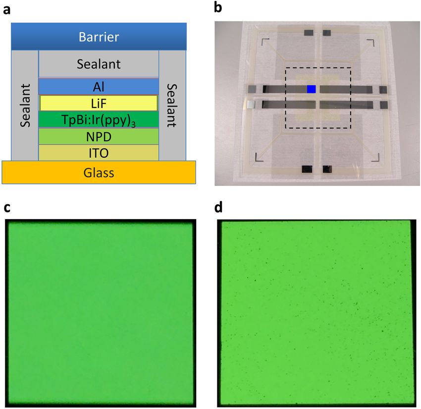
Graphene-based nanolaminates
                                                                      AA Sagade et al.
             2

                 Fig. 1 WVTR measurement. a Optical Ca-test set up utilized for the WVTR measurements. The inset shows a cross-section of the final device
                 stack. b Overview of WVTR values in context of barrier film thickness for various application requirements. The numbers next to square data
                 points are from reported literature references, while star data points are for present study. The dashed line indicates the base value measured
                 for comparative glass barriers fabricated in this investigation along with each batch of graphene-based barriers

                 thin ALD aluminium oxide (AlOx) films. It is found that these             sample reported previously (see Supplementary Table 1). WVTR of
                 nanolaminates show not only lower WVTRs but also more reliable,          such monolayer graphene (G/PEN) is measured to be 0.1 g/m2/
1234567890

                 reproducible performance over large areas compared to simple             day. While this value is comparable to previous reports,20,22 it
                 sequential layering of (transferred) graphene and ALD AlOx. We           should be noted that here our samples (25 cm2) are more than 6
                 demonstrate that these laminates encapsulate OLEDs reasonably            times larger in area (4 cm2). Our results show that monolayer
                 well with measured half-life times of 880 h in ambient.                  graphene and 10 nm of ALD alumina have similar WVTRs.
                                                                                          Regarding further relevant reference samples, we find that neither
                                                                                          a 40 nm ALD alumina coating on monolayer G/PEN nor a
                 RESULTS                                                                  monolayer graphene layer transferred onto a 40 nm AlOx/PEN
                 While WVTRs and barrier performance can be characterized by a            sample lead to any significant barrier performance improvement
                 range of techniques1,4 including MOCON, electrical and optical Ca        relative to the plain 40 nm AlOx/PEN reference. We relate this to
                 tests, etc. for each of them sample compatibility and preparation        defects in the graphene films being not sufficiently decorated/
                 can be a challenge. In particular, for novel material systems like       blocked as well as to the well-known challenge of reliably
                 graphene, reliability and accuracy of the measurements is non-           interfacing with graphene. A similar observation has been made
                 trivial. For meaningful measurements of low WVTRs, here we use           recently by Nam et al.30 Also, we find that the results delicately
                 two independent techniques with low detection limits, namely             depend on process (e.g., growth and transfer) details and hence
                 optical monitoring of Ca film thickness (Fig. 1a) and traceability        we found it difficult to develop a reliable process based on this
                 measurements based on cavity ring down spectroscopy (Supple-             standard route.
                 mentary Fig. 1), as described in the methods section. All results           We therefore establish here a modified growth process as
                 refer to a barrier film size of 5 × 5 cm2, handled and transferred in     highlighted in Fig. 2a. After the initial graphene CVD, we deposit a
                 air unless otherwise stated. As reference, we measure WVTRs of           10 nm AlOx film while the graphene is still on the Cu growth
                 AlOx films of various thicknesses grown by ALD (see methods) on           substrate (G/Cu). We then form a nanolaminate structure by
                 a polyethylene naphthalate (PEN) substrate. The ALD recipe is            carrying out another graphene CVD run onto the AlOx/G/Cu stack.
                 optimized to obtain a highly uniform, good quality film with a            The latter we refer to as second (2nd) growth and the resulting
                 refractive index of 1.65, indicative of high density alumina             structure as re-grown AlOx/graphene (RGA), see Supplementary
                 required for barrier applications.8 These alumina films are used          Fig. 2. In order to assure the initial ALD AlOx coating to be as
                 without further post-treatments such as annealing or O2 plasma.          uniform as possible, we use here a ALD process with 10 water pre-
                 We measure WVTRs for 10 and 40 nm AlOx/PEN films to be 0.1 and            pulses,28,31 which assists the nucleation of AlOx. Figure 3a, b shows
                 8.7 × 10⁻⁴ g/m2/day, respectively, at 22 °C/50% RH (relative             SEM images of the as-deposited 10 nm AlOx film on G/Cu. The
                 humidity). Lower WVTR values have been reported for AlOx, but            AlOx layer is seen to form continuously all over and not selectively
                 only for the alumina layer directly deposited on Ca by in situ           at grain boundaries or defects.27,28 Figure 3c shows cross-sectional
                 glovebox production lines without exposing to ambient.8 Figure           high-resolution TEM (HRTEM) analysis of the RGA structure. The
                 1b provides an overview of WVTR values in the context of barrier         2nd growth leads to additional graphene layer formation beneath
                 film thickness for various application requirements and measured          the AlOx at the existing G/Cu interface, while the AlOx film appears
                 in this study (see Supplementary Table 1 for details on all              to maintain its thickness. The thickness of the resulting graphene
                 samples).                                                                film is ~1 nm, indicating 3–4 layers of graphene. Plan-view TEM
                    Figure 2a is a schematic overview of the process flow used for         and selected area electron diffraction (SAED) measurements of
                 nanolaminate fabrication. Continuous monolayer graphene is               suspended nanolaminates reveal that during the 2nd CVD step
                 grown by CVD (see methods) and transferred via a typical wet             the initially amorphous ALD AlOx layer transforms into a
                 chemical process with PMMA. In the following we refer to this as         nanocrystalline film (Fig. 3d and Supplementary Fig. 3). Interest-
                 standard process (Fig. 2a). The growth parameters are optimized          ingly, the SAED pattern of this nanocrystalline film is not indicative
                 to obtain a large average graphene grain size of 100–200 µm,             of a crystalline Al2O3 phase but best matched to the rarely
                 which (to our knowledge) is larger than any graphene barrier             reported32,33 Al-oxycarbide Al2OC. This suggests structural

                 npj 2D Materials and Applications (2017) 35                               Published in partnership with FCT NOVA with the support of E-MRS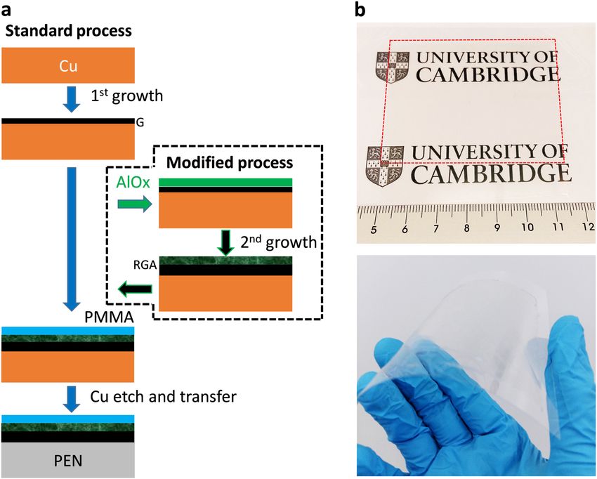
Graphene-based nanolaminates
                                                                       AA Sagade et al.
                                                                                                                                                 3

Fig. 2 Nanolaminate process. a Schematic of the process flow used for graphene and laminate samples. b Optical photographs of large area
7 × 7 cm2 RGA film on PEN substrate highlighting transparency and bendability

changes in the AlOx film upon the 2nd growth step, i.e. Al-             mechanisms of such buried interface graphene is beyond the
oxycarbide formation, hence here-after we refer to the nanocrys-       scope of this work.
talline phase in the RGA film as ‘AlOx-based film’. We emphasize            As a simple initial test of the permeation properties of the RGA
that carrying out a second growth step without the alumina, i.e.       films, we heated them on a hot plate at 200 °C in ambient while
just on the G/Cu, does not lead to the repair of graphene defects,     still on the Cu support along with only monolayer G/Cu and bare
rather at the given CVD conditions destroys the first graphene          Cu foil (Supplementary Fig. 8). The level of Cu oxidation will then
layer during the H2/Ar annealing step or during growth. Hence,         directly reflect the barrier properties of the films. While for Cu and
the process order is important to achieve synergistic effects          G/Cu samples a reddish color is observed within 15–20 s and
between the different materials (See Supplementary Figs. 4 and 5).     30–35 s, respectively, indicative of a rapid Cu oxidation, the RGA/
In the given sequence, the process promotes active bonding/            Cu samples do not show any sign of oxidation even after 30 min of
interaction between the graphene and AlOx-based film (Fig. 3d). In      heating. This is an immediate and positive indication that the RGA
our modified process the 10 nm AlOx layer serves multiple               nanolaminate is uniform and pin-hole free and can act as high-
purposes: (i) it acts as protecting layer to the monolayer graphene    quality moisture barrier.
during the second growth, (ii) it (initially being amorphous and          In contrast to previous reports on graphene barrier films which
not too thick) allows permeation of carbonaceous species for the       aimed at clean graphene layers with minimal polymer contamina-
subsequent second graphene growth at high temperature, (iii)           tion,19,20 here for WVTR measurement study we do not remove
after the second growth it acts as part of an effective                the PMMA layer and utilize it as: (a) protection during Ca oxidation
nanolaminate structure, and iv) it also acts as mechanical support     since Ca is known to form micron scale protrusions which can
in the handling of large-area graphene. Figure 2b shows optical        penetrate through the barrier film and damage it,37,38 (b)
images of such ~10 nm thin RGA layer of 7 × 7 cm2 in size,             insulating layer when used as encapsulation coating for electronic
transferred with PMMA on a PEN substrate. The sample is >90%           devices separating the conductive graphene, and (c) ease of
optically transparent (see Supplementary Fig. 6) and easily            sample handling. We note that the WVTR of 0.3-µm thick PMMA is
bendable (Supplementary Video 1).                                      several orders higher, hence it will not affect on the measured
   The 1st and 2nd growth samples are further probed by Raman          values of graphene-based laminates. In WVTR measurement via
spectroscopy after transfer onto 300 nm SiO2/Si substrates (Fig. 4).   the optical Ca test (see Fig. 1a), the spot size of used laser is large
For the 1st growth, the Raman spectra show an intensity ratio I2D/G    enough to cover cm2 area of sample rather a small spot around
of ∼2–3.7 with a small D peak (ID/G < 0.15) (see Supplementary Fig.    the defects. Hence, the WVTR values correspond to a practical
7) indicative of good quality monolayer graphene. The uniformity       average over the nanolaminate samples. The surface topography
of the growth is highlighted by the I2D/G map in Fig. 4b. On the       of these nanolaminate samples is smooth with a measured rms
other hand, RGA samples show an I2D/G ratio of ∼0.74-1.8 and ID/G      roughness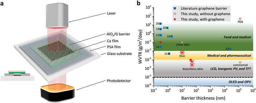
Graphene-based nanolaminates
                                                         AA Sagade et al.
4

    Fig. 3 Mircoscopy of graphene barrier films. a SEM image of continuous growth of 10 nm AlOx on a single graphene grain (dotted area) on Cu
    foil after 1st growth and a representative magnified area in (b). The cross-sectional HRTEM image in c shows the presence of few layer
    graphene below the AlOx-based layer after the 2nd growth, as illustrated in the inset. d Bright field TEM image of a suspended RGA film in
    plan-view, showing the nanocrystalline nature of the AlOx-based phase after the 2nd growth step. The inset shows the corresponding SAED
    pattern, which consists of sets of hexagonally arranged spots assigned to few layer graphene and a ring pattern corresponding to a
    nanocrystalline phase of the Al-oxycarbide Al2OC, as described in Supplementary Fig. 3. e Schematic highlighting the nanolaminate structure
    and coverage of graphene defects by AlOx-based layer. The scale bar in a is 10 μm, b is 0.5 μm, c is 5 nm, and d is 100 nm

    barrier properties of the AlOx (see above),30 the transfer of one       10−4 g/m2/day. The difference might be partly related to the
    PMMA/RGA layer on 40 nm AlOx/PEN showed ~ 3 times improved              distinct sample handling during preparation. This traceability
    performance with a measured WVTR of 2.5 × 10⁻⁴ g/m2/day (see            result is similar to results for 125-µm thick commercial barrier films
    Supplementary Fig. 10 and Table1).                                      which we used as benchmark (multi-stacked layers with few
       To explore the possibility of multi-stack laminates consisting of    microns of mechanical protections; see Fig. 1b and Supplementary
    RGA and AlOx, we focus on a 20 nm AlOx/RGA/20 nm AlOx/PEN               Table 1). In principle, the key mechanism of WVTR improvement in
    structure. Further, we compare the Ca test WVTR values to               the laminates is blocking the moisture paths, therefore sandwich-
    measurements in the traceability set up based on cavity ring down       ing one RGA layer between two AlOx layers (AlOx/RGA/AlOx) is
    spectroscopy. This sandwiched laminate showed a WVTR of 4.4 ×           expected to show improved barrier properties.
    10−3 g/m2/day at 38 °C/90% RH in the Ca test. In comparison, the           In order to validate the adaptability of the introduced RGA
    traceability measurement for such sample gave a value of 6.02 ×         barrier films, we use them here to encapsulate standard OLED

    npj 2D Materials and Applications (2017) 35                             Published in partnership with FCT NOVA with the support of E-MRS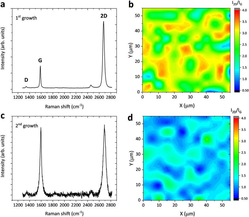
Graphene-based nanolaminates
                                                                       AA Sagade et al.
                                                                                                                                              5

Fig. 4   Spectroscopy of graphene barrier films. Raman spectroscopy of graphene after first (a,b) and second (c,d) growth

devices. The OLED stack (see methods) was made on glass                “sealing” of larger holes in graphene with a simple ALD coverage
substrate and subsequently a PMMA/RGA/PEN barrier was                  is challenging. In line with this previous literature, we show that
laminated onto it without using any additional mechanical              neither an ALD alumina coating onto graphene nor graphene
protection layers, as depicted in Fig. 5a–c and d show optical         transferred onto a AlOx film are reliable and effective means to
images of a 1 × 1 cm2 glowing OLED in ambient, as-fabricated and       straightforwardly achieve synergistic effects to significantly
after 1 week, respectively. For comparison, we also measured two       enhance barrier performance over practically required large areas.
more samples with 40 nm AlOx/PEN and a commercial barrier of           This is due to a range of reasons, including damage of the ALD
125 µm (as studied previously). The OLEDs were lit at 3000 cd/m2       oxide layer during subsequent transfer and poor adhesion of ALD
with 12 V bias and the luminescence measured over time to              oxide layers on the graphene.
extrapolate the half-life time. The observed half-life times of the       Our new route of forming a nanolaminate structure by carrying
40 nm AlOx and commercial barrier of 125 µm are 925 h and 1400         out another graphene CVD run (2nd growth, Fig. 2a) onto an AlOx/
h, respectively, while it is 880 h for ~10 nm RGA, demonstrating       G/Cu structure effectively leads to further graphene layer growth
the successful integration of the transparent RGA structure as         fed by precursor permeation through the existing film. We
effective moisture barrier layer.                                      speculate that important thereby are not only the additional
                                                                       graphene layers but also the “self-formation” of a compact and
                                                                       contiguous structure combining the graphene and AlOx-based
DISCUSSION                                                             film. This is also indicated by the suggested phase transformation
Here, we introduce a nanolaminate structure to improve on the          of the initially amorphous AlOx layer towards a nanocrystalline
shortcomings and challenges of effective large-area barrier            AlOx-based oxycarbide upon the 2nd CVD step (Supplementary
formation via regular sequential layering of (transferred) graphene    Fig. 3). Such RGA layers show WVTRs of 7 × 10⁻³ g/m2/day with
reported previously. These reports have highlighted the chal-          optical transparency of >90% while being only ~10 nm thin, which
lenges of controlled “layering” of transferred graphene including      is significantly better than values reported in previous literature
the deleterious effect of polymer contamination.19,20 A number of      (see Fig. 1b and Supplementary Table 1). This manifests proof-of-
different processes to improve the performance of polymer-based        the-concept effective heterogeneous interfacing. The introduced
barrier layers via the addition of graphene have been reported,39      layer structure could be used as repeat layer unit or as part of a
while O’Hern et al.26 have used polymer and ALD oxide deposition       further multi-layer structure analogue to current commercial
to “seal” practically unavoidable defects in larger-area monolayer     barrier films. Therefore, not only permeation but also a range of
graphene for nanofiltration applications. However, for barrier          other properties can be tuned including adhesion and haze. We
applications, in order to achieve low WVTRs the defects/pinholes       demonstrate one of such a possibility to form multi-layer stacks (of
in graphene cannot be effectively patched by polymers that show        50 nm) by sandwiching RGA layer between two 20 nm thin AlOx
inherent high WVTRs. Hence, a number of reports have looked at         layers which shows superior barrier properties with a WVTR of
the potential of ALD oxides, particularly AlOx, to decorate grain      6.02 × 10⁻⁴ g/m2/day, comparable to values for commercial barrier
boundaries and defects in graphene.27,30 Nevertheless, effective       layers of 125 µm thickness. While our approach is scalable and

Published in partnership with FCT NOVA with the support of E-MRS                             npj 2D Materials and Applications (2017) 35
Graphene-based nanolaminates
AA Sagade et al.
6
Fig. 5 OLED fabrication and encapsulation with RGA barrier. a Schematic of stacks of organic layers in OLED and b final device. Dotted region
shows the RGA barrier of 7 × 7 cm2 and blue box indicates the position of active OLED. Demonstration of glowing OLED of 1 × 1 cm2 area for
the endurance test in ambient: c just after fabrication and d 1 week later
more error-tolerant than previous approaches, high throughput The growth temperature was 970 °C. For the growth, CH4 at 0.1%
manufacturing and handling of very large area ultra-thin films still dilution in Ar was used to obtain a low nucleation density leading to an
requires further innovation to assure high yield (see Supplemen- larger average graphene grain size.40 A chamber pressure of 50 mbar was
tary Fig. 11). In summary, by combining catalytic CVD and ALD we maintained throughout the process.
For the re-growth, 10 nm AlOx was deposited on the G/Cu using a Beneq
have demonstrated >90% transparent, contiguous and bendable TFS 200 atomic layer deposition (ALD) tool. The precursors for Al and
graphene-based nanolaminate barrier films that show WVTRs oxygen were TMA and water, respectively, set at 300 sccm flow rate. A
below 7 × 10⁻³ g/m2/day while being ~10 nm thin and manually conformal growth of AlOx on G/Cu was optimized by utilizing few water
handled in ambient. We systematically benchmarked these WVTRs pulses which act as seed layer for the cyclic growth of the oxide.28,31
compared to existing literature and state-of-the-art barrier films
and demonstrated that the nanolaminate films can be effectively Transfer
integrated in OLEDs enabling half-life times of 880 h in ambient. The grown layers were transferred on planarized 125 µm thick PEN
These results highlight the potential of such heterogeneous substrate (Teijin DuPont Films™, roughnessGraphene-based nanolaminates
AA Sagade et al.
7
90% RH. Traceability measurements were performed at the NPL facility 8. Park, C. Y., An, J. S., Jang, H. J., Lee, J. H. & Choi, B. H. Growth behavior and
with a custom-built set-up based on cavity ring down spectroscopy6 (see improved water-vapor-permeation-barrier properties of 10-nm-thick single Al2O3
Supplementary Fig. 1). In addition, MOCON Aquatran-2 measurements layer grown via cyclic chemical vapor deposition on organic light-emitting
have been carried out for selective reference samples. diodes. Org. Electron. 15, 1717–1723 (2014).
9. Jung, H. et al. Al2O3 multi-density layer structure as a moisture permeation barrier
deposited by radio frequency remote plasma atomic layer deposition. J. Appl.
OLED fabrication Phys. 115, 073502 (2014).
The OLED devices were PHOLED (phosphorescent OLED) with a structure 10. Xiao, W. et al. A flexible transparent gas barrier film employing the method of
consisting of ITO(100 nm)/NPD(100 nm)/(TpBi:Ir(ppy)3)(80/20 nm)/LiF(1.4 mixing ALD/MLD-grown Al2O3 and alucone layers. Nanoscale Res. Lett. 10, 130
nm)/Al(100 nm) on a glass substrate. ITO was used as anode; NPD N,N (2011).
′-Di(1-naphthyl)-N,N′-diphenyl-4,4′-diamine (also known as N,N′-Bis 11. Nakano, Y., Yanase, T., Nagahama, T., Yoshida, H. & Shimada, T. Accurate and
(naphthalen-1-yl)-N,N′-bis(phenyl)benzidine (NPB)), serves as hole trans- stable equal-pressure measurements of water vapor transmission rate reaching
port layer material; TpBi, 1,3,5-tris(N-phenylbenzimidizol-2-yl)benzene was the 10−6 g m−2 day−1 range. Sci. Rep. 6, 35408 (2016).
used as a “Host” doped with a green phosphorescent dopant of Ir(ppy)3, 12. Meyer, J. et al. Al2O3/ZrO2 Nanolaminates as ultrahigh gas-diffusion barriers - A
Tris[2-phenylpyridinato-C2,N]iridium(III), commonly known as a green strategy for reliable encapsulation of organic electronics. Adv. Mater. 21,
phosphorescent emitter; LiF is used as electron injection layer material; 1845–1849 (2009).
and aluminium as a cathode. The whole OLED fabrication was performed 13. Berry, V. Impermeability of graphene and its applications. Carbon 62, 1–10 (2013).
in glovebox. The commercial barrier implemented was from OIKE Co. Ltd. 14. Miao, M., Nardelli, M. B., Wang, Q. & Liu, Y. First principles study of the perme-
ability of graphene to hydrogen atoms. Phys. Chem. Chem. Phys. 15, 16132–16137
Data availability (2013).
15. Tsetseris, L. & Pantelides, S. T. Graphene: An impermeable or selectively perme-
The authors declare that [the/all other] data supporting the findings of this able membrane for atomic species. Carbon 67, 58–63 (2014).
study are available within the paper [and its supplementary information 16. Hofmann, S., Braeuninger-Weimer, P. & Weatherup, R. S. CVD-enabled graphene
files]. Any additional data that support the findings of this study are
manufacture and technology. J. Phys. Chem. Lett. 6, 2714–2721 (2015).
available from the corresponding author upon reasonable request.
17. Wu, T. et al. Fast growth of inch-sized single-crystalline graphene from a con-
trolled single nucleus on Cu–Ni alloys. Nat. Mater. 15, 43–47 (2015).
18. Yan, Z., Peng, Z. & Tour, J. M. Chemical vapor deposition of graphene single
ACKNOWLEDGEMENTS crystals. Acc. Chem. Res. 47, 1327–1337 (2014).
We acknowledge funding via EPSRC-Innovate UK Grant (EP/M507751/1). B.C.B 19. Choi, K. et al. Reduced water vapor transmission rate of graphene gas barrier
acknowledges funding from the European Union’s Horizon 2020 research and films for flexible organic field-effect transistors. ACS Nano 9, 5818–5824 (2015).
innovation program under the Marie Skłodowska-Curie Grant Agreements 656214- 20. Wirtz, C., Berner, N. C. & Duesberg, G. S. Large-scale diffusion barriers from CVD
2DInterFOX. J.C.M. acknowledges support from the Austrian Science Fund (FWF, grown graphene. Adv. Mater. Interfaces 2, 1–5 (2015).
P25721-N20). We thank Philipp Braeuninger-Weimer, James Johnston and Sam Chan 21. Giesbers, A. J. M. et al. Defects, a challenge for graphene in flexible electronics.
for their technical assistance and useful discussions. Solid State Commun. 229, 49–52 (2016).
22. Seo, T. H. et al. Tailored CVD graphene coating as a transparent and flexible gas
barrier. Sci. Rep. 6, 24143 (2016).
AUTHOR CONTRIBUTIONS 23. Seo, H. K. et al. Laminated graphene films for flexible transparent thin film
A.A.S. and S.H. planned the experiments. A.A.S. and A.I.A. carried out growth. S.E., D.B. encapsulation. ACS Appl. Mater. Interfaces 8, (14725–14731 (2016).
and A.A.S. performed Ca tests. S.E. and P.M. carried out OLED experiments. B.G. and P.B. 24. Kim, H. W. et al. Selective gas transport through few-layered graphene and
contributed to traceability measurements. B.C.B. and J.C.M. performed plan-view TEM graphene oxide membranes. Science 342, 91–95 (2013).
and SAED characterization. A.A.S. and S.H. wrote the manuscript with inputs from all 25. Su, Y. et al. Impermeable barrier films and protective coatings based on reduced
authors. graphene oxide. Nat. Commun. 5, 4843 (2014).
26. O’Hern, S. C. et al. Nanofiltration across defect-sealed nanoporous monolayer
graphene. Nano Lett. 15, 3254–3260 (2015).
ADDITIONAL INFORMATION 27. Van Lam, D. et al. Healing defective CVD-graphene through vapor phase treat-
ment. Nanoscale 6, 5639 (2014).
Supplementary information accompanies the paper on the npj 2D Materials and
28. Aria, A. I. et al. Parameter space of atomic layer deposition of ultrathin oxides on
Applications website (https://doi.org/10.1038/s41699-017-0037-z).
graphene. ACS Appl. Mater. Interfaces 8, 30564–30575 (2016).
29. Aria, A. I. et al. Time evolution of the wettability of supported graphene under
Competing interests: The authors declare no competing financial interests.
ambient air exposure. J. Phys. Chem. C 120, 2215–2224 (2016).
30. Nam, T. et al. A composite layer of atomic-layer-deposited Al2O3 and graphene
Publisher's note: Springer Nature remains neutral with regard to jurisdictional claims for flexible moisture barrier. Carbon 116, 553–561 (2017).
in published maps and institutional affiliations. 31. Alexander-Webber, J. A. et al. Hysteresis-free encapsulated CVD graphene tran-
sistors via interface engineering of atomic layer deposited oxide. 2D Mater. 4, 1–9
(2016).
REFERENCES 32. Nakashima, Y., Shirai, T. & Takai, C. Synthesis of aluminum oxycarbide (Al2OC) by
1. Duncan, B., Urquhart, J. & Roberts, S. Review of measurement and modelling of selective microwave heating. J. Ceram. Soc. Jpn. 124, 122–124 (2016).
permeation and diffusion in polymers engineering. NPL Report DEPC MPR 012 33. Ryabkov, Y. I., Grass, V. E. & Sitnikov, P. A. Synthesis of aluminum mono-
(National Physical Laboratory, Middlesex, 2005). oxycarbide. Russ. J. Gen. Chem. 72, 165–167 (2002).
2. Park, J.-S., Chae, H., Chung, H. K. & Lee, S. I. Thin film encapsulation for flexible 34. Wu, Q. et al. Controllable poly-crystalline bilayered and multilayered graphene
AM-OLED: a review. Semicond. Sci. Technol. 26, 34001 (2011). film growth by reciprocal chemical vapor deposition. Nanoscale 7, 10357–10361
3. Lewis, J. S. & Weaver, M. S. Thin-film permeation-barrier technology for flexible (2015).
organic light-emitting devices. IEEE J. Sel. Top. Quantum Electron. 10, 45–57 35. Zhou, H. et al. Chemical vapour deposition growth of large single crystals of
(2004). monolayer and bilayer graphene. Nat. Commun. 4, 2096 (2013).
4. Visweswaran, B. et al. Diffusion of water into permeation barrier layers. J. Vac. Sci. 36. Yao, Y. et al. Controlled growth of multilayer, few-layer, and single-layer graphene
Technol. A 33, 31513 (2015). on metal substrates. J. Phys. Chem. C 115, 5232–5238 (2011).
5. Bird, D. et al. Production and measurement of large-area moisture barriers for 37. Klumbies, H. et al. Thickness dependent barrier performance of permeation
electronic applications. 6th Electronic System-Integration Technology Conference barriers made from atomic layer deposited alumina for organic devices. Org.
(ESTC) 1–6 (IEEE, Grenoble, 2016). Electron. 17, 138–143 (2015).
6. Brewer, P. J., Goody, B. A., Kumar, Y. & Milton, M. J. T. Accurate measurements of 38. Nehm, F. et al. Breakdown and protection of ALD moisture barrier thin films. ACS
water vapor transmission through high-performance barrier layers. Rev. Sci. Appl. Mater. Interfaces 7, 22121–22127 (2015).
Instrum. 83, 75118 (2012). 39. Seethamraju, S. et al. Million-fold decrease in polymer moisture permeability by a
7. Carcia, P. F., McLean, R. S., Reilly, M. H., Groner, M. D. & George, S. M. Ca test of graphene monolayer. ACS Nano 10, 6501–6509 (2016).
Al2O3 gas diffusion barriers grown by atomic layer deposition on polymers. Appl. 40. Braeuninger-Weimer, P., Brennan, B., Pollard, A. J. & Hofmann, S. Under-
Phys. Lett. 89, 3–6 (2006). standing and controlling Cu-catalyzed graphene nucleation: the role of
Published in partnership with FCT NOVA with the support of E-MRS npj 2D Materials and Applications (2017) 35Graphene-based nanolaminates
AA Sagade et al.
8
impurities, roughness, and oxygen scavenging. Chem. Mater. 28, 8905–8915 Commons license, and indicate if changes were made. The images or other third party
(2016). material in this article are included in the article’s Creative Commons license, unless
41. Chen, Y., Gong, X.-L. & Gai, J.-G. Progress and challenges in transfer of large-area indicated otherwise in a credit line to the material. If material is not included in the
graphene films. Adv. Sci. 3, 1500343 (2016). article’s Creative Commons license and your intended use is not permitted by statutory
regulation or exceeds the permitted use, you will need to obtain permission directly
from the copyright holder. To view a copy of this license, visit http://creativecommons.
Open Access This article is licensed under a Creative Commons org/licenses/by/4.0/.
Attribution 4.0 International License, which permits use, sharing,
adaptation, distribution and reproduction in any medium or format, as long as you give
appropriate credit to the original author(s) and the source, provide a link to the Creative © The Author(s) 2017
npj 2D Materials and Applications (2017) 35 Published in partnership with FCT NOVA with the support of E-MRSYou can also read