GS-EVB-HB-66516T-RN TECHNICAL MANUAL - GAN SYSTEMS
←
→
Page content transcription
If your browser does not render page correctly, please read the page content below
GS-EVB-HB-66516T-RN Technical Manual
_____________________________________________________________________________________________________________________

GS-EVB-HB-66516T-RN
Technical Manual

Visit www.gansystems.com for the latest version of this technical manual.

                        DANGER!
                        This evaluation kit is designed for engineering evaluation in a controlled
                        lab environment and should be handled by qualified personnel ONLY.
                        High voltage will be exposed on the board during the test and even brief
                        contact during operation may result in severe injury or death.

                        Never leave the board operating unattended. After it is de-energized,
                        always wait until all capacitors are discharged before touching the board.

                        CAUTION:
                        This product contains parts that are susceptible to damage by electrostatic
                        discharge (ESD). Always follow ESD prevention procedures when
                        handling the product.

GS-EVB-HB-66516T-RN Rev.210219             © 2021 GaN Systems Inc.                     www.gansystems.com               1

                            Please refer to the Evaluation Board/Kit Important Notice on page 27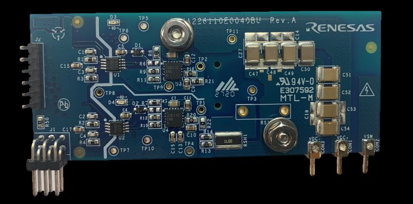
GS-EVB-HB-66516T-RN Technical Manual
_____________________________________________________________________________________________________________________
Overview
The GS-EVB-HB-66516T-RN is RTKA226110DE0040BU RAA226110
https://www.renesas.com/products/raa226110 gate drive demo board. This evaluation kit consists of two
GaN Systems 650V GaN Enhancement-mode HEMTs (E-HEMTs) and all necessary circuits including
half bridge gate drivers, isolated power supplies and optional heatsink to form a functional half bridge
power stage. It allows users to easily evaluate the GaN E-HEMT performance in any half bridge-based
topology, either with the universal mother board (P/N: GS665MB-EVB) or the users’ own system design.
The GS-EVB-HB-66516T-RN demo board provides a -3V turn-off voltage solution. A 0V turn-off solution
is easy to implement as there is no need for a negative power supply rail. For enhancement mode (E-
mode) GaN devices, the Vgs threshold voltage is 1.7V. In order to provide additional noise margin for
demanding applications, the GS-EVB-HB-66516T-RN demo board supplies -3V to the RAA226110 gate
driver. Although this increases the body diode reverse conduction voltage drop compared to a design
with a 0V pull-down, it can still be preferred in high power, high-speed gate drive applications.

Features:

    •    Serves as a reference design and evaluation tool as well as deployment-ready solution for easy in-
         system evaluation.
    •    Vertical mount style with height of 35mm, which fits in the majority of 1U design and allows
         evaluation of GaN E-HEMT in traditional through-hole type power supply boards.
    •    Current shunt position for switching characterization testing
    •    Universal form factor and footprint for all products

The daughter board and universal mother board ordering part numbers are below:
Table 1 Ordering part numbers

    Part Number                   GaN E-HEMT P/N:             Description
    GS-EVB-HB-66516T-                                         GaN E-HEMT 650V/60A, 25mΩ With
                                  GS66516T
    RN                                                        RAA226110 gate driver, -3V turn off voltage
    GS665MB-EVB                                               Universal 650V Mother Board

Control and Power I/Os:
The daughter board GS-EVB-HB-66516T-RN circuit diagram is shown in Figure 1. The control logic
inputs on the 2x3 pin header J1 are listed below:

GS-EVB-HB-66516T-RN Rev.210219             © 2021 GaN Systems Inc.                     www.gansystems.com               2

                            Please refer to the Evaluation Board/Kit Important Notice on page 27
GS-EVB-HB-66516T-RN Technical Manual
_____________________________________________________________________________________________________________________
Table 2 Control pins

   Pin             Descriptipon
   ENABLE          Enable input. It is internally pulled up to VCC, a logic low disables all of the PWM
                   gate drive outputs.
   +5V             +5V auxillary power supply input for logic circuit and gate driver. On the daughter
                   board there are 2 isolated 5V to 9V DC/DC power supplies for top and bottom
                   switches.
   VDRV            Not used. VDRV can be connected to VCC though R43. R43 is DNP by default.
   PWMH_IN         High side PWM logic input for top switch Q1. It is compatible wth 3.3V and 5V
   PWML_IN         Low side PWM logic input for bottom switch Q2. It is compatible wth 3.3V and 5V
   0V              Logic inputs and gate drive power supply ground return.

The 3 power pins are:
    • VDC+: Input DC Bus voltage
    • VSW: Switching node output
    • VDC-: Input DC bus voltage ground return. Note that control ground 0V is isolated from VDC-

VCC

ENABLE                             Iso . DC /DC

PWMH                                                                                                  VDC +
                                     Isolator         RAA226110                 Q1
PWML
                                    IL611-1E          Gate Driver

                                   Iso . DC /DC
                                                                                                      VSW

                                      Isolator        RAA226110                 Q2         C4 - 10
                                     IL611-1E         Gate Driver

                                                                                 shunt                VDC -

                       Figure 1 GS-EVB-HB-66516T-RN Evaluation Board Block Diagram

GS-EVB-HB-66516T-RN Rev.210219             © 2021 GaN Systems Inc.                     www.gansystems.com               3

                            Please refer to the Evaluation Board/Kit Important Notice on page 27
GS-EVB-HB-66516T-RN Technical Manual
_____________________________________________________________________________________________________________________
GS-EVB-HB-66516T-RN half bridge daughter board

                                                                                                            B
                                                                         A

                     C
                                                                               E
                                                                    F
                                       D

                                    Figure 2 GS-EVB-HB-66516T-RN top side

                                        Heat sink location

                                                                                                                G

                                  Figure 3 GS-EVB-HB-66516T-RN bottom side

    A.   2x GaN Systems 650V E-HEMT GS66516T, 60A/25mΩ.
    B.   Decoupling capacitors C14-C17 and C47-C54.
    C.   Signal isolator IL611-1E.
    D.   GaN driver RAA226110.
    E.   OCP shunt.
    F.   TP1(gate) and TP4(source) test points for bottom Q2 VGS.
    G.   5V-12V isolated DC/DC gate drive power supply

GS-EVB-HB-66516T-RN Rev.210219             © 2021 GaN Systems Inc.                     www.gansystems.com               4

                            Please refer to the Evaluation Board/Kit Important Notice on page 27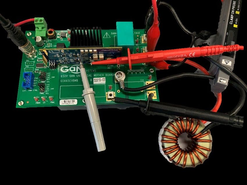
GS-EVB-HB-66516T-RN Technical Manual
_____________________________________________________________________________________________________________________
GaN E-HEMTs:
    •    This daughter board includes two GaN Systems E-HEMT GS66516T, 60A/25mΩ in a GaNPx™ B
         type package. The large S pad serves as source connection and thermal pad. Pin 4 is the kelvin
         source connection for gate drive return.

                                      Figure 4 Package outline of GS66516T

Gate driver circuit:
    •    Renesas RAA226110 low-side gate driver is chosen for this design. This driver provides 5.8V gate
         drive with 3.8V UVLO. It supports the 5.8V turn on and -3V/0V turn off. It has separated source
         and sink drive outputs which eliminates the need for an additional diode. OCP is also integrated
         in the driver.
    •    RAA226110 provides a configurable source current(0.3A/0.75A/2A) to adjust the slew rate of
         GS66516T without gate resistor to minimize the gate loop. The turn off speed can be directly
         controlled by the gate resistor Rg_off (R22).

                                             Figure 5 Gate driver circuit
Gate drive power supply:
    •    5V-12V isolated DC/DC converters are used for gate drive. The RAA226110 accepts 4.5V to 18V
         VDD input voltage.

GS-EVB-HB-66516T-RN Rev.210219             © 2021 GaN Systems Inc.                     www.gansystems.com               5

                            Please refer to the Evaluation Board/Kit Important Notice on page 27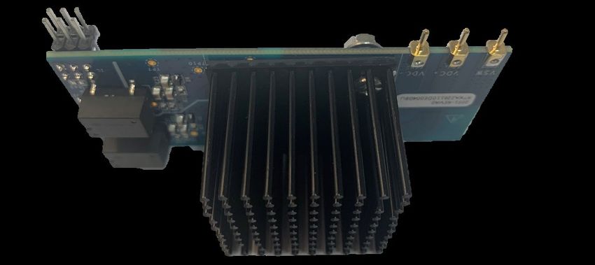
GS-EVB-HB-66516T-RN Technical Manual
_____________________________________________________________________________________________________________________

                                         Figure 6 Gate drive power supply

Current shunt:
    •    The board provides an optional current shunt position E (Figure2) between the source of Q2 and
         power ground return. This allows drain current measurement for switching characterization test
         such as Eon/Eoff measurement.

Circuit modification for current shunt
    •    To properly measure device current with current shunt, the OCP function has to be disabled by
         removing resistor R13 and R14, and make connection to short pin 7(ISNSN) and pin 8(ISNSP) of
         the RAA226110, as shown in figure 7.
    •    The shunt resistor RSH1 also needs to be removed.

                             Figure 7 Circuit modification for current measurement

Measurement with current shunt:

    1.   When measuring VSW with current shunt, ensure all channel probe grounds and current shunt
         BNC output case are all referenced to the source end of Q2 before the current shunt. The
         recommended setup of probes is shown as below.

GS-EVB-HB-66516T-RN Rev.210219             © 2021 GaN Systems Inc.                     www.gansystems.com               6

                            Please refer to the Evaluation Board/Kit Important Notice on page 27
GS-EVB-HB-66516T-RN Technical Manual
_____________________________________________________________________________________________________________________
    2.   The output of coaxial current shunt can be connected to oscilloscope via 50Ω termination
         impedance to reduce the ringing.
    3.   The measured current is inverted and can be scaled by using: Id=Vid/Rshunt.

                         Figure 8 Recommended probe connection with current shunt
Thermal design:

    1.   GS66516T has a thermal pad at the top side for heat dissipation.
    2.   A heatsink (35x35mm size) can be attached to the top side of board for optimum cooling. Thermal
         Interface Material (TIM) is needed to provide electrical insulation and conformance to the top of
         the GaN device surface. The daughter board evaluation kit is shipped with a sample 35x35mm
         fin heatsink (not installed), although other heatsinks can also be used to fit users’ system design.
    3.   A thermal tape type TIM (Berguist® Bond-Ply 100) is chosen for its easy assembly. The supplied
         heatsink has the thermal tape pre-applied so simply peel off the protective film and attach the
         heatsink to the back of board as marked in Figure 3.
    4.   Two optional mounting holes as shown in Figure 9 are provided for mounting customized
         heatsink using screws.
    5.   Using the supplied heatsink and TIM, the overall junction to ambient thermal resistance RthJ-A is
         ~9°C/W with 500LFM airflow.
    6.   Forced air cooling is recommended for power testing.

GS-EVB-HB-66516T-RN Rev.210219             © 2021 GaN Systems Inc.                     www.gansystems.com               7

                            Please refer to the Evaluation Board/Kit Important Notice on page 27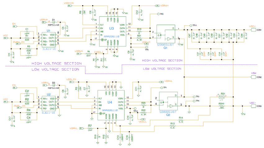
GS-EVB-HB-66516T-RN Technical Manual
_____________________________________________________________________________________________________________________
Figure 9 The daughter board with heatsink attached
CAUTION:
There is no on-board over-temperature protection. Device temperature must
be closely monitored during testing. Never operate the board with device
temperature exceeding TJ_MAX (150°C)
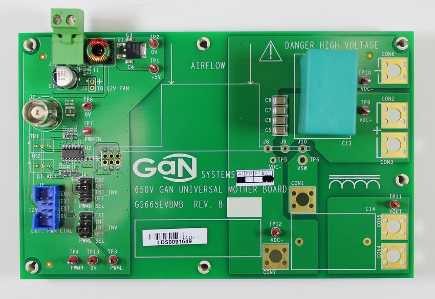
Using GS-EVB-HB-66516T-RN with universal mother board GS665MB-EVB
12V INPUT
Airflow direction
(+)
5V Power Supply
VDC-
CIN
For Ext. Daughter Board
12VDC Fan VDC+
Probing point for VSW
VSW
PWM control & dead VDC- VOUT
Optional Cout
time circuit
Figure 10 650V universal mother board GS665MB-EVB
GaN Systems provides a universal 650V mother board (ordering part number: GS665MB-EVB, sold
separately) that can be used as the basic evaluation platform for all the daughter boards.
GS-EVB-HB-66516T-RN Rev.210219 © 2021 GaN Systems Inc. www.gansystems.com 8
Please refer to the Evaluation Board/Kit Important Notice on page 27
GS-EVB-HB-66516T-RN Technical Manual
_____________________________________________________________________________________________________________________
The universal 650V mother board evaluation kit includes following items:
    1. Mother board GS665MB-EVB
    2. 12VDC Fan

12V input:
The board can be powered by 9-12V on J1. On-board voltage regulator creates to 5V for daughter board
and control logic circuits. J3 is used for external 12VDC fan.

PWM control circuit:

                                    Figure 11 PWM control input and dead time circuit
                                                +5V

                                                         C9

                                                        0.1uF
                                                        C10
   J7                             TP7     U2A
                                              14

                                                        1uF
112538                     R1
         1                                1                                                                           U2B
                                                                         0V                   D1 PMEG2005EB
                                                              3                                                  4                    R3
                           49R9           2                                                                                      6
                     R2
5
4
3
2

             R4                                                                                    SOD523        5
                     100R                                         D2 PMEG2005EB                                                       49R9
             100R                               74VHC132                                          R5
                     R1206
                                              7

             R1206
                     DNP                                                                                             74VHC132        PWM
             DNP                   TP8                                 SOD523
                                                                                               1K00
                                                                                                                                     OUTPUT
                                                                                             2K    TR1                C11
                                                                        R6
                                                                                                                      100pF
                                                                                                    DNP
                                                                       1K00
                                                                  2K      TR2
    0V                                          0V
                                                                                                  U2C            0V U2D
                                                                        DNP          C12     9                    12                  R7
                                                                                     100pF                   8                   11
                                                                                             10                  13
                                                                                                                                      49R9
                                                                                0V                                                   INVERTED
                                                                                                  74VHC132            74VHC132
                                                                                                                                     PWM OUTPUT
                             Figure 12 On board dead time generatrion circuit
The top and bottom switches PWM inputs can be individually controlled by two jumpers J4 and J6. Users
can choose between a pair of complementary on-board internal PWM signals (non-inverted and inverted,
controlled by J7 input) with dead time or external high/low side drive signals from J5 (users’ own control
board).

GS-EVB-HB-66516T-RN Rev.210219                        © 2021 GaN Systems Inc.                             www.gansystems.com                  9

                                  Please refer to the Evaluation Board/Kit Important Notice on page 27
GS-EVB-HB-66516T-RN Technical Manual
_____________________________________________________________________________________________________________________
An on-board dead time generation circuit is included on the mother board. Dead time is controlled by
two RC delay circuits, R6/C12 and R5/C11. The default dead time is set to about 100ns. Additionally two
potentiometer locations are provided (TR1/TR2, not included) to allow fine adjustment of the dead time if
needed.

               WARNING!
               ALWAYS double check the jumper setting and PWM gate drive signals
               before applying power. Incorrect PWM inputs or jumper settings may cause
               device failures

Test points:
Test points are designed in groups/pairs to facilitate probing:

  Test points             Name                               Description
  TP1/TP2                 +5V/0V                             5V bias power
  TP7/TP8                 PWMIN/0V                           PWM input signal from J7
  TP4/TP3/TP13            PWMH/PWML/0V                       High/low side gate signals to daughter board
  TP9/TP10                VDC+/VDC-                          DC bus voltage
  TP11/TP12               VOUT/VDC-                          Output voltage
  TP6/TP5                 VSW/VDC-                           Switching node output voltage (for HV oscilloscope
                                                             probe)

Power connections:

CON1-CON7 mounting pads are designed to be compatible with following mounting terminals:
  • #10-32 Screw mount,
  • Banana Jack PCB mount (Keystone P/N: 575-4), or
  • PC Mount Screw Terminal (Keystone P/N: 8191)

Output passives (L and C14)

An external power inductor (not included) can be connected between VSW (CON1) and VOUT (CON4/5)
or VDC+ (CON2/3) for double pulse test. Users can choose their inductor size to meet the test
requirement. Generally it is recommended to use a power inductor with low inter-winding capacitance to
obtain best switching performance. For the double pulse testing we use 2x 60uH/40Amp inductor (CWS,
P/N: HF467-600M-40AV) in series. C14 is designed to accommodate a film capacitor as output filter.

GS-EVB-HB-66516T-RN Rev.210219             © 2021 GaN Systems Inc.                    www.gansystems.com                10

                            Please refer to the Evaluation Board/Kit Important Notice on page 27
GS-EVB-HB-66516T-RN Technical Manual
_____________________________________________________________________________________________________________________
Double pulse test mode
CON3
VDC+ PWM +5V
INPUT
CON2 (J7)
LOUT 0V
+6V
+ Q1
IL VGL
VDS 0V
400V DC VSW
VDS
CON1 CON4 CON5
ISW
Q2
VGL
CON6 CON7
IL
VDC-
TON1
t0 t1 t2 t3
Figure 13 Double pulse test setup
Double pulse test allows easy evaluation of device switching performance at high voltage/current
without the need of actually running at high power. It can also be used for switching loss (Eon/Eoff)
measurement and other switching characterization parameter test.
The circuit configuration and operating principle can be found in Figure 13:
1. The output inductor is connected to the VDC+.
2. At t0 when Q2 is switched on, the inductor current starts to ramp up until t1. The period of first
pulse Ton1 defines the switching current ISW = (VDS*TON1) / L.
3. t1-t2 is the free wheeling period when the inductor current IL forces Q1 to conduct in reverse.
4. t1 (turn-off) and t2 (turn-on) are of interest for this test as they are the hard switching transients
for the half bridge circuit when Q2 is under high switching stress.
5. The second pulse t2-t3 is kept short to limit the peak inductor current at t3.
The double pulse signal can be generated using a programmable signal generator or microcontroller/DSP
board. As this test involves high switching stress and high current, it is recommended to set the double
pulse test gate signal as single trigger mode or use long repetition period (for example >50-100ms) to
avoid excess stress on the switches. Q1 can be kept off during the test or driven synchronously (J4 set to
OFF or INT_INV) and Q2 is set to INT (or EXT position if PWM signal is from J5).
WARNING!
Limit the maximum switching test current to 30A and ensure maximum drain
voltage including ringing is below 650V for pulse testing. Exceeding this limit
may cause damage to the devices.
GS-EVB-HB-66516T-RN Rev.210219 © 2021 GaN Systems Inc. www.gansystems.com 11
Please refer to the Evaluation Board/Kit Important Notice on page 27GS-EVB-HB-66516T-RN Technical Manual
_____________________________________________________________________________________________________________________
Buck/Standard half bridge mode
CON3 This is standard half bridge configuration that can be used in
VDC+
following circuits :
CON2
LOUT • Synchronous Buck DC/DC
+ Q1 • Single phase half bridge inverter
CON5
• ZVS half bridge LLC
400V DC VSW CON4
CON1 • Phase leg for full bridge DC/DC or
Q2
COUT RLoad • Phase leg for a 3-phase motor drive
Jumper setting:
CON6
VDC- • J4 (Q1): INT
CON7 • J6 (Q2): INT_INV
Boost mode
When the output becomes the input and the load is
VDC+
attached between VDC+ and VDC-, the board is
CON2 CON3 converted into a boost mode circuit and can be used for:
LIN
• Synchronous Boost DC/DC
Q1
• Totem pole bridgeless PFC
CON5 VIN
VSW CON4 Jumper setting:
CON1 • J4 (Q1): INT_INV
Q2
INPUT
• J6 (Q2): INT
CON6
CON7
VDC-
GS-EVB-HB-66516T-RN Rev.210219 © 2021 GaN Systems Inc. www.gansystems.com 12
Please refer to the Evaluation Board/Kit Important Notice on page 27GS-EVB-HB-66516T-RN Technical Manual
_____________________________________________________________________________________________________________________
Using GS-EVB-HB-66516T-RN in system:
The daughter board allows users to easily evaluate the GaN performance in their own systems. Refer to
the footprint drawing of GS-EVB-HB-66516T-RN as shown below:
8 9
1 3 5 7
2 4 6
1. All units are in mm.
2. Pin 1-6: Dia. 1mm
3. Pin 7-9: 1.91mm (75mil) mounting hole for Mill-max Receptacle P/N: 0312-0-15-15-34-27-10-0.
Figure 14 Recommended footprint drawing of daughter board GS665XXX-EVBDB
GS-EVB-HB-66516T-RN Rev.210219 © 2021 GaN Systems Inc. www.gansystems.com 13
Please refer to the Evaluation Board/Kit Important Notice on page 27GS-EVB-HB-66516T-RN Technical Manual
_____________________________________________________________________________________________________________________
Quick Start procedure –Pulses test
Follow the instructions below to quickly get started with your evaluation of GaN E-HEMT. Equipment
and components you will need:
• Four-channel oscilloscope with 500MHz bandwidth or higher
• high bandwidth (500MHz or higher) passive probe
• high bandwidth (500MHz) high voltage probe (>600V)
• AC/DC current probe for inductor current measurement
• 12V DC power supply
• Signal generator capable of creating testing pulses
• High voltage power supply (0-400VDC) with current limit.
• External power inductor (recommend toroid inductor 50-200uH)
1. Check the position E (figure2) on daughter board GS-EVB-HB-66516T-RN.
2. Install GS-EVB-HB-66516T-RN on the mother board. Press all the way down until you feel a click.
Connect probe between TP8 (low side GaN gate) and TP3 (low side GaN source) for gate voltage
measurement in the daughter board.
3. Set up the mother board:
a. Connect 12VDC bias supply to J1.
b. Connect PWM input gate signal (0-5V) to J7. If it is generated from a signal generator ensure
the output mode is high-Z mode.
c. Set J4 to OFF position and J7 to INT.
d. Set High voltage (HV) DC supply voltage to 0V and ensure the output is OFF. Connect HV
supply to CON2 and CON6.
e. Use HV probe between TP6 and TP5 for Vds measurement.
f. Connect external inductor between CON1 and CON3. Use current probe to measure inductor
current IL.
4. Set up and check PWM gate signal:
a. Turn-on 12VDC power.
b. Check the 2 LEDs on the daughter board. They should be turned on indicating the isolated
9V is present.
c. Set up signal generator to create the waveforms as shown in Figure 13. Use equation ISW =
(VDS*TON1) / L to calculate the pulse width of the first pulse and ensure the Isw_max is ≤40A at
400VDC.
d. Set the operation mode to either single trigger or Burst mode with repetition period of 100ms.
e. Turn on the PWM output and check on the oscilloscope to make sure the GaN gate drive
voltage waveform is present and matches the PWM input.
5. Power-on:
a. Turn on the output of the HV supply. Start with low voltage and slowly ramp the voltage up
until it reaches 400VDC. During the ramping period closely observe the the voltage and
current waveforms on the oscilloscope.
6. Power-off:
GS-EVB-HB-66516T-RN Rev.210219 © 2021 GaN Systems Inc. www.gansystems.com 14
Please refer to the Evaluation Board/Kit Important Notice on page 27GS-EVB-HB-66516T-RN Technical Manual
_____________________________________________________________________________________________________________________
a. After the test is complete, slowly ramp down the HV supply voltage to 0V and turn off the
output. Then turn off the 12V bias supply and signal generator output.
12VDC Vdc+/Vdc-
PWM in
Inductor
Figure 15 Pulses test setup example
GS-EVB-HB-66516T-RN Rev.210219 © 2021 GaN Systems Inc. www.gansystems.com 15
Please refer to the Evaluation Board/Kit Important Notice on page 27GS-EVB-HB-66516T-RN Technical Manual
_____________________________________________________________________________________________________________________
Test results – GS66516T-EVBDB
Pulses test (VDS=400V, IMAX = 33A, Lp=120uH, RG(ON)=0Ω, Igsel is connected to VDRV , Gate driver current is 0.3A,
RG(OFF)=1Ω, 8 pulses, periode=4us, duty=40%):
Vds_low side
I_inductor
V_gate
I_inductor
V_ds_L
V_gate
Figure 16 400V/33A pulses test waveform
Figure 16 shows the hard switching on waveforms at 400V/33A. A Vds dip can be seen due to the rising
drain current (di/dt in the power loop ΔV=Lp*di/dt, where Lp is the total power loop inductance). After
the drain current reaches the inductor current, the Vds starts to fall. The Vgs undershoot spike is caused
by the miller feedback via Cgd under negative dv/dt.
GS-EVB-HB-66516T-RN Rev.210219 © 2021 GaN Systems Inc. www.gansystems.com 16
Please refer to the Evaluation Board/Kit Important Notice on page 27GS-EVB-HB-66516T-RN Technical Manual
_____________________________________________________________________________________________________________________
Due to the low gate charge and small RG(OFF) , GaN E-HEMT gate has limited control on the turn-off
dv/dt. Instead the Vds rise time is determined by how fast the turn-off current charges the switching
node capacitance (Coss).
The low Coss of GaN E-HEMT and low parasitic inductance of the GaNPX™ package, together with an
optimized PCB layout, enables a fast and clean turn-off. Even with dv/dt greater than 100V/ns, expect
only 50V of overshoot on the turn-off Vds waveform. The measured rise time is 4ns at 400V and 33A hard
turn-off.
The OCP setpoint is 40A. Due to ringing on the current sensing signal, the actual OCP trigger point is 33A. After
the OCP occurs, the driver will be locked with Gate pulled low regardless of the PWM input. To reset the OCP,
the gate driver power supply must be restarted.
Synchronous Buck Test (L=120uH, VIN=400V, VOUT=80V, D=20%, FSW=100 kHz, POUT =300W)
V_ds_L
I_inductor
PWM
Figure 17 Buck test waveform (Pout=300W)
GS-EVB-HB-66516T-RN Rev.210219 © 2021 GaN Systems Inc. www.gansystems.com 17
Please refer to the Evaluation Board/Kit Important Notice on page 27GS-EVB-HB-66516T-RN Technical Manual
_____________________________________________________________________________________________________________________
Appendix A – GS-EVB-HB-66516T-RN
Circuit schematics
GS-EVB-HB-66516T-RN Rev.210219 © 2021 GaN Systems Inc. www.gansystems.com 18
Please refer to the Evaluation Board/Kit Important Notice on page 27GS-EVB-HB-66516T-RN Technical Manual
_____________________________________________________________________________________________________________________
Assembly Drawing
GS-EVB-HB-66516T-RN Rev.210219 © 2021 GaN Systems Inc. www.gansystems.com 19
Please refer to the Evaluation Board/Kit Important Notice on page 27GS-EVB-HB-66516T-RN Technical Manual
_____________________________________________________________________________________________________________________
PCB layout
Top Layer
Mid Layer 1
GS-EVB-HB-66516T-RN Rev.210219 © 2021 GaN Systems Inc. www.gansystems.com 20
Please refer to the Evaluation Board/Kit Important Notice on page 27GS-EVB-HB-66516T-RN Technical Manual
_____________________________________________________________________________________________________________________
Mid Layer 2
Bottom Layer
GS-EVB-HB-66516T-RN Rev.210219 © 2021 GaN Systems Inc. www.gansystems.com 21
Please refer to the Evaluation Board/Kit Important Notice on page 27GS-EVB-HB-66516T-RN Technical Manual
_____________________________________________________________________________________________________________________
Bill of Materials
Item Part
Quantity Value PCB Footprint
Number Reference
1 1 16PF C1 CAP_0603
2 1 16PF C2 CAP_0603
3 1 16PF C3 CAP_0603
4 1 16PF C4 CAP_0603
5 1 0.1UF C5 CAP_0603
6 1 0.1UF C6 CAP_0603
7 1 0.1UF C7 CAP_0603
8 1 0.1UF C8 CAP_0603
9 1 4.7UF C9 CAP_0603
10 1 4.7UF C10 CAP_0603
11 1 4.7UF C11 CAP_0603
12 1 4.7UF C12 CAP_0603
13 1 1000PF C13 CAP_0603
14 1 1UF C14 CAP_2220
15 1 0.1UF C15 CAP_0603
16 1 1000PF C16 CAP_0603
17 1 0.1UF C17 CAP_0603
18 1 1UF C18 CAP_2220
19 1 4.7UF C19 CAP_0805
20 1 4.7UF C20 CAP_0805
21 1 4.7UF C21 CAP_0805
22 1 4.7UF C22 CAP_0805
23 1 4.7UF C23 CAP_0805
24 1 4.7UF C24 CAP_0805
25 1 4.7UF C25 CAP_0805
26 1 4.7UF C26 CAP_0805
27 1 1UF C27 CAP_2220
28 1 0.1UF C47 CAP_1812
29 1 0.1UF C48 CAP_1812
30 1 0.1UF C49 CAP_1812
31 1 0.1UF C50 CAP_1812
32 1 0.1UF C51 CAP_1812
33 1 0.1UF C52 CAP_1812
34 1 0.1UF C53 CAP_1812
35 1 0.1UF C54 CAP_1812
36 1 TEST_POINT CON1 TP-48S125P
37 1 TEST_POINT CON2 TP-48S125P
38 1 TEST_POINT CON3 TP-48S125P
39 1 SM_SCHOTTKY D1 SOD323
40 1 SM_SCHOTTKY D2 SOD323
41 1 SM_LED D3 LED_LTST-C190KGKT
42 1 SM_LED D4 LED_LTST-C190KGKT
43 1 MM3Z9V1ST1G D5 SOD323
44 1 MM3Z9V1ST1G D6 SOD323
45 1 ATS_54350X HS1 HSK_COOL_ATS-54350X-C1-R0_MT2
46 1 CONN6 J1 CON_HDR_3X6_100_RA
GS-EVB-HB-66516T-RN Rev.210219 © 2021 GaN Systems Inc. www.gansystems.com 22
Please refer to the Evaluation Board/Kit Important Notice on page 27GS-EVB-HB-66516T-RN Technical Manual
_____________________________________________________________________________________________________________________
47 1 CONN6 J2 CONN-1X6
48 1 GS66516T Q1 GAN_TRANSISTOR_GS66516T
49 1 GS66516T Q2 GAN_TRANSISTOR_GS66516T
50 1 820 R1 RES_0603
51 1 820 R2 RES_0603
52 1 820 R3 RES_0603
53 1 820 R4 RES_0603
54 1 10K R5 RES_0603
55 1 DNP R6 RES_0603
56 1 DNP R7 RES_0603
57 1 10K R8 RES_0603
58 1 0 R9 RES_0603
59 1 0 R10 RES_0603
60 1 1M R11 RES_0603
61 1 1M R12 RES_0603
62 1 5.6 R13 RES_0603
63 1 5.6 R14 RES_0603
64 1 0 R19 RES_0603
65 1 0 R20 RES_0603
66 1 3.3K R21 RES_0603
67 1 3.3K R22 RES_0603
68 1 3.3K R28 RES_0603
69 1 3.3K R29 RES_0603
70 1 3.3K R30 RES_0603
71 1 3.3K R31 RES_0603
72 1 1K R32 RES_0603
73 1 1K R33 RES_0603
74 1 DNP R43 RES_0603
75 1 3.3K R50 RES_0603
76 1 .1 RS1 RES_SHUNT_SDN-XXX
77 1 .001 RSH1 RES_RHOM_PML100
78 1 TEST_POINT TP1 TP_41C60P
79 1 TEST_POINT TP2 TP_41C60P
80 1 TEST_POINT TP3 TP_41C60P
81 1 TEST_POINT TP4 TP_41C60P
82 1 TEST_POINT TP5 TP_41C60P
83 1 TEST_POINT TP6 TP_41C60P
84 1 TEST_POINT TP7 TP_41C60P
85 1 TEST_POINT TP8 TP_41C60P
86 1 TEST_POINT TP9 TP_41C60P
87 1 TEST_POINT TP10 TP_41C60P
88 1 TEST_POINT TP11 TP_41C60P
89 1 IL611 U1 MSOP8_118_256
90 1 IL611 U2 MSOP8_118_256
91 1 RAA226110 U3 QFN16_157X157_256_EP
92 1 RAA226110 U4 QFN16_157X157_256_EP
93 1 PES1 U5 PKG_CUI_5-8PIN_8P3MMX11P20MM
94 1 PES1 U6 PKG_CUI_5-8PIN_8P3MMX11P20MM
GS-EVB-HB-66516T-RN Rev.210219 © 2021 GaN Systems Inc. www.gansystems.com 23
Please refer to the Evaluation Board/Kit Important Notice on page 27U1 +5V
J1 VAUX +12V TP1
MC7805
Circuit schematics
1 T1 1 3
4
3
IN OUT FOOTPRINT FOR GS665XX-EVBDB
GND
C1
C2 C3
2 220uF 25V C4 +5V VCC
10u
4
CAPAL-PANA-F 1uF 25V 10u
C0805 TP2
1
2
C0805
CMC-08 J2 +5V
VAUX 12V IN TP4 ENABLE
PWMH_IN 1 2 VDRV
PWNL_IN 3 4
VAUX_RTN J4 5 6
1 0V TP3
2 1 PWM_EXT_H
GS-EVB-HB-66516T-RN Rev.210219
2 +5V PWM_INT 0V
J5 PWM_INT_INV
J3 TP5 VDC- 1
J8
Appendix B - GS665MB-EVB
TO 12V FAN 1 2
3 4 C5 C6 C7
+12V TP13 C8 1
5 6 J6 0.1uF 1kV J9
7 8 0V
PWM_EXT_L C1812 VDC+
PWM_INT VSW 1
PWM_INT_INV J10
0V 0V
0V TP6
1
+5V EXTERNAL PWM INPUT
TO DSP/MCU CONTROL BOARD 0V
C9
PWM INPUT SELECTION VSW
0.1uF POS 1: EXT. PWM SIGNAL
C10
CON1
J7 TP7 U2A POS 2/3: INTERNAL PWM SIGNAL
14
1uF
112538 R1
1 1 U2B
0V D1 PMEG2005EB POS 4: OFF
3 4 R3
49R9 2 6
5
4
3
2
R2 5
R4 SOD523
100R D2 PMEG2005EB 49R9
100R 74VHC132 R5
7
R1206
R1206
© 2021 GaN Systems Inc.
DNP 74VHC132 PWM VDC_P CON5
DNP 1K00 CON4
TP8 SOD523 OUTPUT CON2 CON3
2K TR1 C11
R6
100pF
DNP
1K00 VOUT
2K TR2
0V 0V
1
U2C 0V U2D
1
TP11
1
1
DNP C12 9 12 R7 TP-KEY STONE-5010
100pF 8 11 TP9
10 13 VDC+ VOUT
49R9
0V INVERTED TP-KEY STONE-5010
74VHC132 74VHC132
PWM OUTPUT
C13 C14 TP12
ON BOARD DEAD TIME GENERATION CIRCUIT TP-KEY STONE-5010
10uF 700V 10uF 700V
USE TR1 AND TR2 TO ADJUST DEAD TIME TP10
VDC- DNP
TP-KEY STONE-5010
Please refer to the Evaluation Board/Kit Important Notice on page 27
NOTES - UNLESS OTHERWISE SPECIFIED
1
1
1. ALL SMD RESISTORS AND CAPACITORS ARE 0603 SIZE M1 M2 M3 M4
2. DO NOT INSTALL TR1,TR2,R2,R3 AND C14
VDC_N
PCB STANDOFF 4.75MM MNT HOLE CON7
www.gansystems.com
CON6
KEYSTONE 8839-8834
_____________________________________________________________________________________________________________________
GS-EVB-HB-66516T-RN Technical Manual
24GS-EVB-HB-66516T-RN Technical Manual
_____________________________________________________________________________________________________________________
Assembly drawing
Assembly Top
Assembly Bottom
GS-EVB-HB-66516T-RN Rev.210219 © 2021 GaN Systems Inc. www.gansystems.com 25
Please refer to the Evaluation Board/Kit Important Notice on page 27GAN SYSTEMS 650V GAN UNIVERSAL MOTHER BOATRD
BOARD P/N: GS665EVBMB
Bill of Materials
Revision B1
Last Update 6/30/2016
Quantity Reference Description Value Manufacturer Part number Assembly Note
1 PCB PCB bare 2-layer 2oz Cu.
CON1,CON2,CON3,CON4,C
1 7 ON5,CON6,CON7 TERMINAL SCREW VERTICAL PC MNT CON-10-32-SCRWMNT KEYSTONE 8191 DO NOT INSTALL
2 1 C1 CAP ALUM 220UF 20% 25V SMD 220uF 25V Panasonic EEE-FK1E221P
GS-EVB-HB-66516T-RN Rev.210219
3 1 C2,C10 GENERIC 1UF/25V, 10% X7R SMD 0603 1uF TAIYO YUDEN TMK107B7105KA-T
4 2 C3,C4 GENERIC 10UF/25V, 10% SMD 0805 10uF TAIYO YUDEN TMK212BBJ106KG-T
5 4 C5,C6,C7,C8 GENERIC 0.1uF/1000V, SMD 1812 0.1uF 1kV KEMET C1812C104KDRAC7800
6 1 C9 GENERIC 0.1UF/25V, 10% X7R SMD 0603 0.1uF TAIYO YUDEN TMJ107BB7104KAHT
7 2 C11,C12 GENERIC 100PF/25V 5% NP0 SMD 0603 100pF KEMET C0603C101J3GACTU
CAP FILM 10UF/600VDC 5%, 27.5MM LEAD
8 1 C13,C14 SPACING 10uF 700V KEMET C4AEHBU5100A11J DO NOT INSTALL C14
9 2 D1,D2 DIODE SCHOTTKY 20V 500MA SOD523 PMEG2005EB NXP PMEG2005EB,115
10 1 J1 TERM BLOCK HDR 2POS R/A 5.08MM CON-TERM-BLK-2POS-RA TE CONNECTIVITY 796638-2
11 1 J1-PLUG TERM BLOCK BLUG 2POS 5.08MM TE CONNECTIVITY 796634-2
12 1 J2 CONN RCPT 6POS .100 DBL STR PCB CON-RCPT-2X3-BOT HARWIN M20-7850342 MOUNT FROM BOTTOM SIDE
CONNECTOR FOR 12V FAN, DO NOT
13 1 J3 CON-2POS INSTALL
14 2 J4,J6 CONN HEADER 8POS DUAL VERT PCB CON-JMP-4POS HARWIN M20-9980445
© 2021 GaN Systems Inc.
15 1 J5 CONN 8-POS, DUAL ROW 2.54MM CON-HDR-4X2 AMPHENOL 75869-132LF
16 1 J7 CONN BNC JACK STR 50 OHM PCB 112538 AMPHENOL 112538
MATING SOCKET FOR MILLMAX
17 3 J8,J9,J10 CONN RECEPT PIN .032-.046" .075" CON-RCPT-EDGEMNT MILLMAX 0312-0-15-15-34-27-10-0 EDGE MNT PIN
18 3 R1,R3,R7 generic 1% smd 0603 49R9 VISHAY DALE CRCW060349R9FKEA
19 2 R2,R4 generic 1% smd 1206 100R DO NOT INSTALL
20 2 R5,R6 generic 1% snd 0603 1K00 VISHAY DALE CRCW06031K00FKEA
TP1,TP2,TP3,TP4,TP7,TP8,
21 11 TP9,TP10,TP11,TP12,TP13 TEST POINT PCB TP-KEYSTONE-5010 KEYSTONE 5010
22 2 TR1,TR2 2K RECOM CMC-08 DO NOT INSTALL
23 1 T1 COMM MODE CHOKE 5.2A T/H CMC-08
Please refer to the Evaluation Board/Kit Important Notice on page 27
24 1 U1 IC REG LDO 5V 1A DPAK MC7805 ON SEMI MC7805BDTRKG
25 1 U2 1 IC GATE NAND 4CH 2-INP 14-SOIC 74VHC132 FAIRCHILD 74VHC132MX
Off the board components:
PCB SPACER, INSTALL FROM
26 6 M1,M2,M3,M4,M5,M6 PCB STANDOFF NYLON STACKABLE 4.75M MECH-STDOFF-KEYSTONE-88KEYSTONE 8833 BOTTOM SIDE
SUPPLY LOOSE, DO NOT INSTALL
www.gansystems.com
27 1 FAN FAN AXIAL 38X20MM 12VDC WIRE SUNON FANS PMD1238PKB1-A.(2).GN ON THE ASSEMBLY
INSTALL ON J4 "INT" POSITION AND
28 2 JUMPER JUMPER SHUNT GENERIC TE CONNECTIVITY 382811-8 J6 "INT_INV" POSITION
_____________________________________________________________________________________________________________________
GS-EVB-HB-66516T-RN Technical Manual
26GS-EVB-HB-66516T-RN Technical Manual
_____________________________________________________________________________________________________________________
Evaluation Board/kit Important Notice
GaN Systems Inc. (GaN Systems) provides the enclosed product(s) under the following AS IS conditions:
This evaluation board/kit being sold or provided by GaN Systems is intended for use for ENGINEERING
DEVELOPMENT, DEMONSTRATION, and OR EVALUATION PURPOSES ONLY and is not considered by GaN
Systems to be a finished end-product fit for general consumer use. As such, the goods being sold or provided are
not intended to be complete in terms of required design-, marketing-, and/or manufacturing-related protective
considerations, including but not limited to product safety and environmental measures typically found in end
products that incorporate such semiconductor components or circuit boards. This evaluation board/kit does not fall
within the scope of the European Union directives regarding electromagnetic compatibility, restricted substances
(RoHS), recycling (WEEE), FCC, CE or UL, and therefore may not meet the technical requirements of these directives,
or other related regulations.
If this evaluation board/kit does not meet the specifications indicated in the User’s Guide, the board/kit may be
returned within 30 days from the date of delivery for a full refund. THE FOREGOING WARRANTY IS THE
EXCLUSIVE WARRANTY MADE BY THE SELLER TO BUYER AND IS IN LIEU OF ALL OTHER WARRANTIES,
EXPRESSED, IMPLIED, OR STATUTORY, INCLUDING ANY WARRANTY OF MERCHANTABILITY OR FITNESS
FOR ANY PARTICULAR PURPOSE. EXCEPT TO THE EXTENT OF THIS INDEMNITY, NEITHER PARTY SHALL
BE LIABLE TO THE OTHER FOR ANY INDIRECT, SPECIAL, INCIDENTAL, OR CONSEQUENTIAL DAMAGES.
The user assumes all responsibility and liability for proper and safe handling of the goods. Further, the user
indemnifies GaN Systems from all claims arising from the handling or use of the goods. Due to the open construction
of the product, it is the user’s responsibility to take any and all appropriate precautions with regard to electrostatic
discharge.
No License is granted under any patent right or other intellectual property right of GaN Systems whatsoever. GaN
Systems assumes no liability for applications assistance, customer product design, software performance, or
infringement of patents or any other intellectual property rights of any kind.
GaN Systems currently services a variety of customers for products around the world, and therefore this
transaction is not exclusive.
Please read the User’s Guide and, specifically, the Warnings and Restrictions notice in the User’s Guide prior to
handling the product. Persons handling the product(s) must have electronics training and observe good
engineering practice standards.
This notice contains important safety information about temperatures and voltages. For further safety concerns,
please contact a GaN Systems’ application engineer.
GS-EVB-HB-66516T-RN Rev.210219 © 2021 GaN Systems Inc. www.gansystems.com 27
Please refer to the Evaluation Board/Kit Important Notice on page 27GS-EVB-HB-66516T-RN Technical Manual
_____________________________________________________________________________________________________________________
In Canada: In Europe: In the United States:
GaN Systems Inc. GaN Systems Ltd., German Branch GaN Systems Corp.
1145 Innovation Drive Suite 101 Terminalstrasse Mitte 18, 2723 South State Street, Suite 150,
Ottawa, Ontario, Canada K2K 3G8 85356 München, Germany Ann Arbor, MI. USA 48104
T +1 613-686-1996 T +49 (0) 8165 9822 7260 T +1 248-609-7643
www.gansystems.com
Important Notice – Unless expressly approved in writing by an authorized representative of GaN Systems, GaN Systems components are not designed, authorized or
warranted for use in lifesaving, life sustaining, military, aircraft, or space applications, nor in products or systems where failure or malfunction may result in personal injury,
death, or property or environmental damage. The information given in this document shall not in any event be regarded as a guarantee of performance. GaN Systems hereby
disclaims any or all warranties and liabilities of any kind, including but not limited to warranties of non-infringement of intellectual property rights. All other brand and product
names are trademarks or registered trademarks of their respective owners. Information provided herein is intended as a guide only and is subject to change without notice.
The information contained herein or any use of such information does not grant, explicitly, or implicitly, to any party any patent rights, licenses, or any other intellectual
property rights. General Sales and Terms Conditions apply.
© 2009-2015 GaN Systems Inc. All rights reserved.
GS-EVB-HB-66516T-RN Rev.210219 © 2021 GaN Systems Inc. www.gansystems.com 28
Please refer to the Evaluation Board/Kit Important Notice on page 27You can also read