Instytut Technologii Elektronowej
←
→
Page content transcription
If your browser does not render page correctly, please read the page content below
Instytut Technologii Elektronowej

    Research Activities and Opportunities
     for Collaboration (Division of Silicon
 Microsystem and Nanostructure Technology)
                                                                                                Dr. Tomasz Bieniek
  1
                                   Tomasz Bieniek, Grzegorz Janczyk
Successful R&I in Europe 2019 - 10th European Networking Event am 14-15.02.2019 in Düsseldorf   tbieniek@ite.waw.pl
Instytut Technologii Elektronowej (ITE)
Institute of Electron Technology (ITE) is a public, Polish, non-profit research organization,
located in Warsaw (Piaseczno, Krakow), Poland, carrying out applied research and close-
to-market innovation (TRL 3 to 8) in microelectronics, photonics and microsystem domain.

      Photonics      Integrated      Micro-      Si- Microsystem      Micro- and      Materials and       Design and       Certification
                      Circuits     Electronics          and        Nanotechnology    Semiconductor      diagnostics of
                    and Systems     (Krakow)      Nanostructure    of Wide Bandgap     Structures         electronic
                       Design                      Technology      Semiconductors      Research

                  *
                                                                                                      nanostructures and
                                                   (Piaseczno)                                           components

 The mission of the Institute is to conduct the basic and applied rese-
 arch in the field of semiconductor electronics and physics in order to
 develop and commercialize innovative micro- and nanotechnologies
 and their applications in semiconductor microelectronics, optoelec-
 tronics, photonics and micromechanics.
 * Integrated Circuits & Systems Development – the R&D Activities and Collaboration Opportunities for customized sensor networks, power electronics
 and telemedicine by G. Janczyk, session ICT, 14:15, room Amsterdam 1
                                                                                                                                           Dr. Tomasz Bieniek
Successful R&I in Europe 2019 - 10th European Networking Event am 14-15.02.2019 in Düsseldorf                                              tbieniek@ite.waw.pl
  2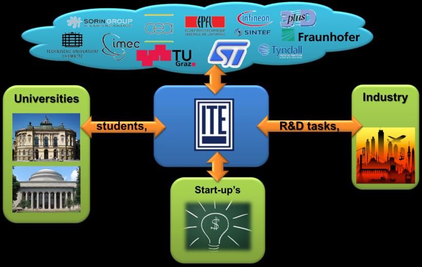
Area of Interest & R&D Domains
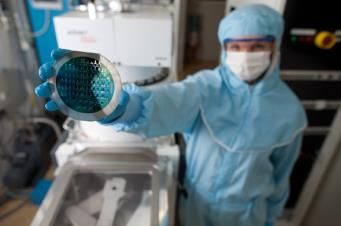
Silicon technological R&D line with full CMOS and MEMS processes:
• Total Clean Room Area approx. 1200 sq. m. , • Silicon wafers – mainly 100mm and 150mm
• Cleanliness class 1000 and 100 up to 10 (lithography) • Lithography linewidth 0.9 µm (e-beam 30-100nm)
R&D Domains: Full set of CMOS/MEMS technology &
• MEMS/MOEMS devices based on silicon micromachining measurement equipment including:
• Sensors and Actuators (based on silicon and non-silicon • Full Photolithography cluster (incl. 3D photoresist
technology) deposition)
• Advanced CMOS (FDSOI) technologies • Laser mask & direct writing tool.,
• Silicon micro- and nano-probes • Mask shop (mask fabrication, up to 6”)
• Bio-compatible microelectrodes for medical implants • Deep Silicon RIE (bosch process, cryo proc.)
• MEMS/MOEMS design, modeling & simulation • Plasma cluster (etching, PECVD, 5 reactors)
• Customer specific detectors and photodiodes (incl. • Thermal processes cluster (ox.; diff; anneal)
avalanche) • Metallization cluster (Al, alloys, Au, Pt, Ti, Cr, others)
• Energy harvesting devices (mechanical, thermal, photo) • CVD cluster (incl. LPCVD, low. temp. dep)
• Integration of various silicon and non-silicon micro- • Assembly cluster (cutting/wire & die bonders)
technologies • Wet chemistry processing cluster (clean/etching)
• Characterization (optical, electrical, mechanical, etc…) • Ion implantation (ion beam, immersion plasma)
• Assembling, bonding, heterogenous integration • Characterization & diagnostic (opto, elect. SEM, …)
We are FLEXIBLE & customer oriented !!!!
Dr. Tomasz Bieniek
Successful R&I in Europe 2019 - 10th European Networking Event am 14-15.02.2019 in Düsseldorf tbieniek@ite.waw.pl
3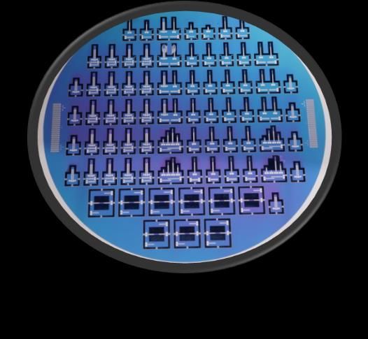
Area of Interest and Partner Profiles
  Offered activities:
  •   Partnership in research (H2020, ECSEL, bilateral) – ICT, materials, IoT, power
  •   Partnership in business
  Our role: partner, coordinator, subcontractor, R&D
  Specialized services in:
  •   Design (product, module, component), synthesis
  •   Technology processing
  •   Measurements, characterization
  •   Packaging, assembly, integration
  •   Testing
  •   Low volume production
  Prototype technology for specialized devices:
  •   Sensors, detectors, microsystems, readout IC
  •   Signal processing
  •   Data processing etc…
  •   Certification services

                                                                                                Dr. Tomasz Bieniek
Successful R&I in Europe 2019 - 10th European Networking Event am 14-15.02.2019 in Düsseldorf   tbieniek@ite.waw.pl
  4
Reference projects:
 Centrum Nanoelektroniki, Mikrosystemów i Fotoniki, Wykorzystanie działalności badawczo-rozwojowej w
 gospodarce (Strategia rozwoju Polski Centralnej do roku 2020 z perspektywą 2030, 2018 – 2020, 70MPLN
 ~16MEuro)
 REACTION - first and euRopEAn siC eigTh Inches pilOt line (2018 – 2022) ECSEL H2020
 R3-PowerUP - 300mm Pilot Line for Smart Power and Power Discretes (2017 - 2021) ECSEL H2020
 Lab4MEMS-II - Micro-Optical MEMS, micro-mirros and pico-projectors (2014 – 2018) ENIAC JU (ECSEL)
 SESBE - Smart Elements for Sustainable Building Envelopes (2013 2017) FP7
 CarriCool - Modular Interposer System Architecture providing scalable Heat Removal, …(2014 – 2017) FP7
 Lab4MEMS - LAB FAB for smart sensors and actuators MEMS (2013 – 2016) ENIAC JU (ECSEL)
 Nanoheat - MultidomaiN plAtform for iNtegrated MOre-tHan-MoorE/Beyond CMOS systems … (2012 – 2016) FP7
 SIMS - Scientific Infrastructure Management Support (2013 – 2015) Operational Programmes Human Capital
 SMAC - SMArt systems Co-design (2011 – 2015) FP7
 PARSIMO - Partitioning and modelling of system-in-package (2011 – 2014) ENIAC JU (ECSEL)
 SmartFrame (2011 – 2014) ERDF
 e-BRAINS - Best-Reliable Ambient Intelligent Nano Sensor Systems (2010 – 2014) FP7
 Nano-Tec - Nano Ecosystems Technology and Design for Nanoelectronics (2010 – 2013) FP7
 MINTE – Mikrosystemy i nanotechnologie elektroniczne dla innow. gosp. (2009 – 2013) POIG
 MNS-DIAG - Mikro- i Nano Systemy w Chemii i Diagnostyce Biomedycznej (2007 – 2013) POIG
 CORONA - Customer-Oriented Product Engineering of Micro and Nano Devices (2008 – 2011) FP7
 SE2A - Nanoelectronics for Safe, Fuel Efficient and Environment Friendly Autom. Sol. (2009 – 2011)
 e-CUBES, INTEGRAMplus, SUCIMA…..
 and many more: http://www.ite.waw.pl/en/projekty/european-projects/

                                                                                                          Dr. Tomasz Bieniek
Successful R&I in Europe 2019 - 10th European Networking Event am 14-15.02.2019 in Düsseldorf             tbieniek@ite.waw.pl
  5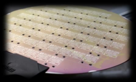
Instytut Technologii Elektronowej
   Division of Silicon Microsystem and Nanostructure Technology
   Dr. Tomasz Bieniek
   tel.: +48 22 279 32 00
   email: tbieniek@ite.waw.pl

   Department of Integrated Circuits and Systems Design
   Dr. Grzegorz Janczyk
   Tel.: +48 22 548 78 50
   email: janczyk@ite.waw.pl

                                     www.ite.waw.pl
                https://www.youtube.com/user/ElectronTechnology

                                                                                                Dr. Tomasz Bieniek
Successful R&I in Europe 2019 - 10th European Networking Event am 14-15.02.2019 in Düsseldorf   tbieniek@ite.waw.pl
  6
You can also read