Net Ties and How to Use Them
←
→
Page content transcription
If your browser does not render page correctly, please read the page content below
Net Ties and How to Use Them

Summary
                      The Net Tie is a component type which allows for shorting together various nets in
                      a design. The graphic for the symbol can be as simple as two component pins
                      representing a virtual component between nets or as complex as mutipul pins (as
                      many as desired) to connect mutipul nets together with complex graphics to
                      elaborate on the specific application. Specifying the componet Type as Net Tie
                      allows placing copper features between PCB footprint pads in order to facilitate
                      connecting (shorting) various nets together at very specific locations on the PCB.

                      Some examples of where to use a Net Tie component would be (however not
                      limited to) connecting two polygons of differing ground nets together at a specific
                      place (AGND and DGND for instance), connecting mutipul nets together for length
                      tuning, or allowing component pads to be intially shorted together, later removing
                      the shorting copper for placemant of an actual component. Applications are limited
                      only to the imagine of the circuit designer; some of them will be explored here.

Question:
What is a Net Tie and how can it be used?

Procedure:
Defining a Net Tie component is simply a matter of specifying Net Tie in the Type field of the Component
Properties dialog.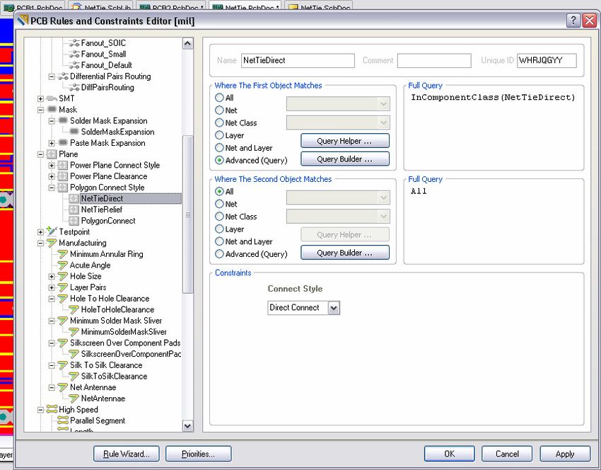
There are two types of Net Ties, Net Tie and Net Tie (In BOM). Each type is available on the pull down
options for Type in the Component Properties dialog. When using a Net Tie the component schematic
symbol graphic is attached to a specific type of footprint containing copper features connecting (shorting)
the pads together. Net connectivity between the schematic symbol pins and PCB footprint pads is
established in the customary way; however, no line item will appear for this component in the Bill Of
Materials (BOM). Using the Net Tie (In BOM) allows materials such as two pin headers to be called out in
the BOM. Both types will be explored in this How To document.

The simplest form of a net tie is a two pin component associated with a two pad footprint in which the
pads are connected together with copper features.

As with other schematic symbol Types, the                (Below) A Net Tie Footprint possibly used to
display of symbol pin designators and display            short two polygons of differing net names.
names are optional, schematic wiring between
pins determines net connectivity, and there is a
pin to pad connectivity established between the
schematic and PCB. The graphic for a Net Tie
component is arbitrary and in some cases
unnecessary. For instance a two pin Net Tie
component may be represented to look like a
piece of wire in a schematic sheet (totally hiding
its existence).

                                                         (Below) Net Tie In BOM used to designate a two
                                                         pin header with the pins initially shorted together.
                                                         This component would call out the header part in
                                                         the BOM. The shorting copper may be removed
                                                         at a later date to allow the application of an
                                                         optional shorting jumper.

Examples of two pin Net Tie Schematic Symbols
While routing to the pads of a Net Tie footprint the Design Rule Checks (DRC) allows routing the nets associated with each pad to other same net copper features without flagging a violation; allowing the connecting (shorting) copper feature of the footprint to connect the two differing nets. If the two track ends from differing nets short together across the footprint the DRC will flag a violation. This is due to the short circuit being generated between two differing nets outside the constraints of the Net Tie footprint. Net Tie components allow establishing a connection between two differing nets at and only at the location of the of the Net Tie footprint on the PCB. The DRC will flag any other short circuit violation between these differing nets elsewhere in the design. Below: Net Ties can be setup to allow routing two differing nets together with various track widths.
Below: Net Tie components can be created to allow routing between various routing layers by
incorporating through hole (Multilayer) pads.

Below: Net Tie footprints can be created to allow shorting between nets and later the shorting copper
may be removed allowing components to be placed between nets. In this example there is an 0805 and
a 0602 footprint placed on top of each other with a shorting copper feature placed between them. This
will allow the designer options for component placement at a later time. In this example the short may be
replaced with a surface mount resistor or inductor.
Planar inductors pose a special challenge. When various windings of the inductor are placed directly on
the PCB each winding is composed of routing tracks creating the various inductor coils. Each coil is a
continuous copper track with differing nets at each end of the winding. The inductor winding track
typically introduces a short circuit between each of the nets on the ends of the winding resulting in a DRC
violation.

The solution that Altium Designer provides is to place a Net Tie component in series with the inductor
windings. This provides a means of connecting differing nets, one net representing the winding and one
side of the electrical circuit and the other net being the second electrical connection.

Below: Is a circuit bridging two differing ground nets with a planar inductor winding. The Net Tie
component provides a means of tying AGND to the EGND net which is extant through out the planar
winding.

In this example silkscreen and reference designators have been shown to illustrate the placement of the
components, however, these features may be left off the actual design to elevate clutter and confusion in
a high density design.
Net Tie components may be used to connect polygons of differing nets to allow shorting at one and only
one place. Other short circuits between these two nets will be flagged a violations by the DRC.
In the following example multiple Net Tie
components have been placed on a PCB to
illustrate how design rules can be scoped to
specify polygon connect style in order to achieve
the desired result.
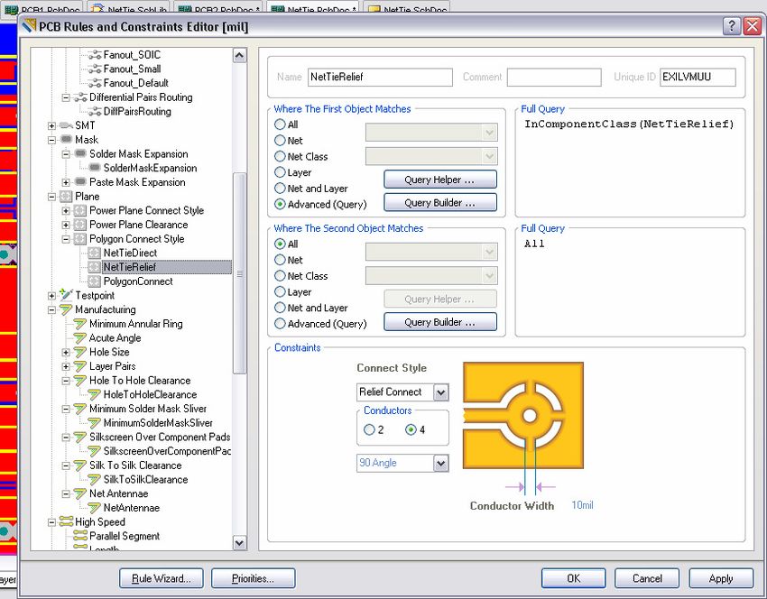
Here nets NT5, NT6, NT7, NT8, and NT 11 have
been placed in a Component Class labeled
NetTieDirect.
Nets NT1, NT2, NT3, NT4, and NT10 have been
placed in a Component Classed labeled
NetTieRelief.Two Polygon Connect style rules have been created for the example NetTieDirect and NetTieRelief
which are scoped to the Component Classes NetTieDirect and NetTieRelief respectively.
In the upper area of the PCB the Net Ties are
connected to the polygons following the Relief
connect rule. Note that NT1 has a polygon
connect on the left side and the DRC allows
routing from the right pad to the polygon.
The lower portion of the PCB follows the direct
connect style. Notice how the polygon pulls back
from the connecting (shorting) copper feature
according to the clearance rules.Net Ties may have an unlimited number of pins and pads electrically connecting an unlimited number of
nets.
Right: Examples of multi-pin Net Tie schematic
symbols.
Below: Extreme example of what can be
achieved with Net Tie footprints.
Net length tuning provides an interesting challenge when the signal path of time critical signals must
arrive at the load end of the net at the same time within a reasonable delta. In the example below the
clock signal is generated and routed to two different IC packages. It is critical that the signal path of this
high speed signal have achieve the same length within a reasonable tolerance.The use of a multi-net Net Tie allows the net to be broken out into separate nets for the purpose of length tuning. Below: The associated footprint allows the same signal to travel different net paths. The nets CK1 and CK2 are associated into a Net Class labeled CLK and a Length rule is then created for this class.
Once the nets CK1 and CK2 have been routed they can be length tuned to the Length rule which
specifies the total length and tolerance.

Conclusion:
The Net Tie is a unique component type allowing the engineer and PCB designer alike the flexibility to
short different nets together allowing the flexibility to handle a variety of design challenges. Their
application is limited only by the imagination.

Corporate Headquarters       United States           Switzerland                  Germany                    France                         The Netherlands          China
Altium Inc.                  Altium Inc.             Altium Inc.                  Altium Inc.                Altium Inc.                    Altium Inc.              Altium Inc.
3 Minna Close                3207 Grey Hawk Court    Bundesplatz 2                Philipp-Reis-Strasse 3     121 rue d'Aguesseau            Goorseweg 5              9C, East Hope Plaza
Belrose NSW 2085 Australia   Suite 100               Postfach 4525                D-76137 Karlsruhe          F-92100 Boulogne-Billancourt   7475 BB Markelo          No. 1777 Century Avenue
Phone: +61 2 8622 8100       Carlsbad, CA 92010      CH-6304 Zug                  Germany                    France                         The Netherlands          Shanghai 200122, P.R.China
Fax: +61 2 8622 8140         Phone: 1-800-544-4186   Switzerland                  Phone: 49 0 721 8244 300   Tel: +33 (0)1 55 60 23 70      Phone: +31 547 33 4045   China
                             Fax: 1-760-231-0761     Phone: +41 (0) 800 880 506   Fax: 49 0 721 8244 320     Fax: +33 (0)1 55 60 18 39      Fax: +31 84 22 812 57    Phone: +86 21 6182 3900
North America Support                                Fax: +41 (0) 848 258 486                                                                                        Fax: +86 21 6876 4015
800 488 0681
You can also read