VMK180 Evaluation Board - User Guide UG1411 (v1.0) January 7, 2021 - Xilinx
←
→
Page content transcription
If your browser does not render page correctly, please read the page content below
VMK180 Evaluation Board

User Guide
UG1411 (v1.0) January 7, 2021
Revision History

Revision History
       The following table shows the revision history for this document.

                            Section                                     Revision Summary
                                              01/07/2021 Version 1.0
        Initial release.                                 N/A

UG1411 (v1.0) January 7, 2021                                                          www.xilinx.com
                                                                       Send Feedback
VMK180 Board User Guide                                                                             2
Table of Contents
       Revision History...............................................................................................................2

       Chapter 1: Introduction.............................................................................................. 5
           Overview.......................................................................................................................................5
           Navigating Content by Design Process.................................................................................... 6
           Additional Resources.................................................................................................................. 7
           Block Diagram..............................................................................................................................8
           Board Features............................................................................................................................ 9
           Board Specifications................................................................................................................. 12

       Chapter 2: Board Setup and Configuration....................................................13
           Standard ESD Measures........................................................................................................... 13
           Board Component Location.....................................................................................................13
           Default Jumper and Switch Settings....................................................................................... 17
           Versal ACAP Configuration.......................................................................................................21

       Chapter 3: Board Component Descriptions................................................... 23
           Overview.....................................................................................................................................23
           Component Descriptions......................................................................................................... 23

       Appendix A: VITA 57.4 FMCP Connector Pinouts......................................... 70
           Overview.....................................................................................................................................70

       Appendix B: Xilinx Design Constraints............................................................. 71
           Overview.....................................................................................................................................71

       Appendix C: Pmod FMC..............................................................................................72
           Pin Mapping Pmod to FMC...................................................................................................... 73

       Appendix D: Regulatory and Compliance Information...........................75
           CE Information...........................................................................................................................75
           Compliance Markings............................................................................................................... 76

UG1411 (v1.0) January 7, 2021                                                                                                      www.xilinx.com
                                                                                                     Send Feedback
VMK180 Board User Guide                                                                                                                         3
Appendix E: Additional Resources and Legal Notices..............................77
          Xilinx Resources.........................................................................................................................77
          Documentation Navigator and Design Hubs.........................................................................77
          References..................................................................................................................................78
          Please Read: Important Legal Notices................................................................................... 79

UG1411 (v1.0) January 7, 2021                                                                                                   www.xilinx.com
                                                                                                   Send Feedback
VMK180 Board User Guide                                                                                                                      4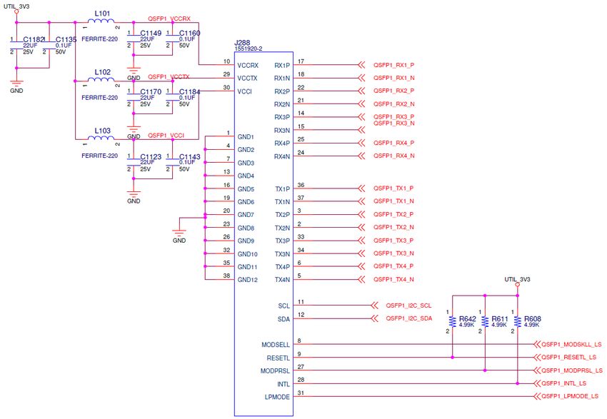
Chapter 1: Introduction

                                                                                  Chapter 1

Introduction

Overview
       The VMK180 evaluation board features the Xilinx® Versal™ ACAP XCVM1802 device. The
       VMK180 board enables the demonstration, evaluation, and development of the applications
       listed here, as well as other customer applications.

       • Storage acceleration
       • Data center network acceleration
       • Passive optical network
       • Automotive
       • Aerospace and defense
       • Industrial, scientific, and medical
       • Test and measurement
       • Embedded vision
       • Machine learning
       • Audio video broadcast
       • Wired and wireless

       The VMK180 evaluation board is equipped with many of the common board-level features
       needed for design development, including:

       • SFP28 and QSFP28 optical transceiver support
       • LPDDR4 component and DDR4 UDIMM memory
       • HDMI
       • USB
       • PMOD connectors
       • CAN and Ethernet networking interfaces
       • Two FMC+ expansion ports

UG1411 (v1.0) January 7, 2021                                                       www.xilinx.com
                                                                  Send Feedback
VMK180 Board User Guide                                                                          5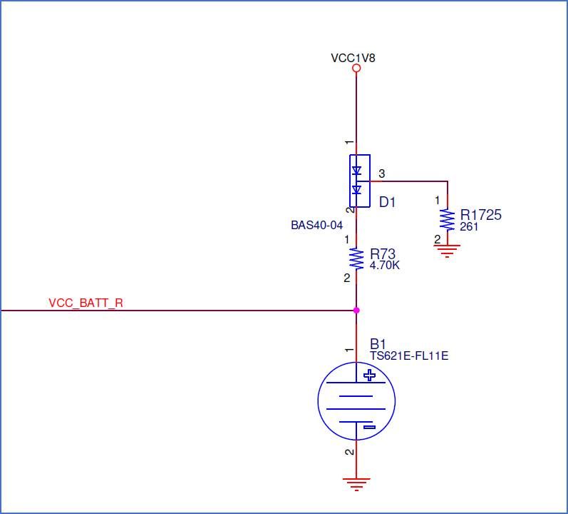
Chapter 1: Introduction

       • PCIe® (up to Gen4x8)

       Models of VMK180 Boards
       The following table lists the models for the VMK180 evaluation board. See the VMK180
       Evaluation Board product page for details.

       The following table lists the models for the VMK180 evaluation board. See the VMK180
       Evaluation Board product page for details.

       Table 1: Models of VMK180 Evaluation Boards

                             Kit                                                                                   Description
                                                                    Xilinx Versal ACAP VMK180 evaluation kit, encryption disabled, no secure boot
        EK-VMK180-G-ED
                                                                    support
        EK-VMK180-G-ED-J                                            Xilinx Versal ACAP VMK180 evaluation kit, Japan specific

       Versal ACAP Kit Numbering
       The Versal ACAP kit numbering is illustrated in the following figure.

                                                                      Figure 1: Kit Numbering

                                                             Product Number

                        EK                 -         VM              K         180            -         G          -   ED    -       J
                                                                                                       ROHS                        Regional
                          Kit
                                                                                   Silicon indicator Indicator                     Identifier
                         Type
                                                                         K = kit
                                               Family and series         Ensures there is no
                                               (e.g., Versal ACAP        confusion with silicon P/Ns
                       Options
                                               and Core)
                  EK – Evaluation Kit
                                                                Examples                                Options                     Options
               CK – Characterization Kit
                                                                VCK190                                 G – ROHS                    J – Japan
                                                                VMK 180                                Compliant                 ED – All other
                                                                                                                                   customers
                                                                                                                                 OEM – OEM kit

                                                                                                                                                   X24959-010421

Navigating Content by Design Process
       Xilinx® documentation is organized around a set of standard design processes to help you find
       relevant content for your current development task. This document covers the following design
       processes:

UG1411 (v1.0) January 7, 2021                                                                                                                     www.xilinx.com
                                                                                                                       Send Feedback
VMK180 Board User Guide                                                                                                                                        6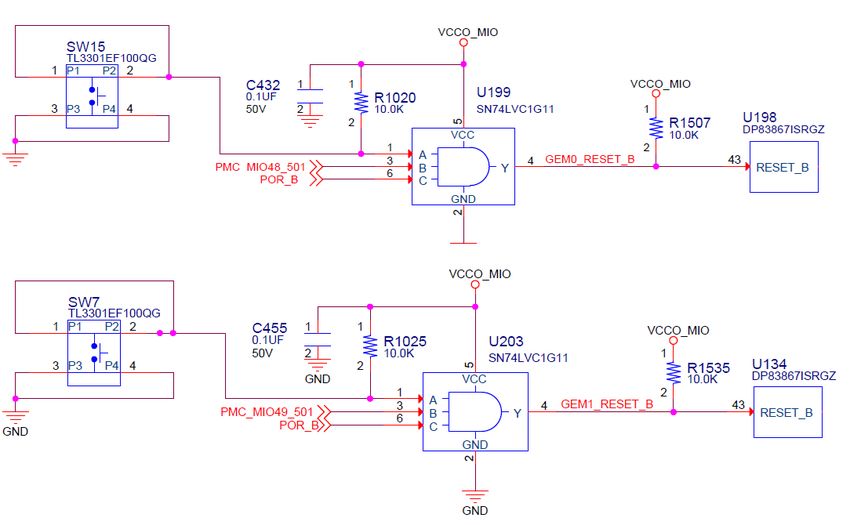
Chapter 1: Introduction

       • Board System Design: Designing a PCB through schematics and board layout. Also involves
         power, thermal, and signal integrity considerations. For more information, see Versal ACAP
         Design Process Documentation Board System Design.

Additional Resources
       See Appendix E: Additional Resources and Legal Notices for references to documents, files, and
       resources relevant to the VMK180 evaluation board.

UG1411 (v1.0) January 7, 2021                                                           www.xilinx.com
                                                                    Send Feedback
VMK180 Board User Guide                                                                              7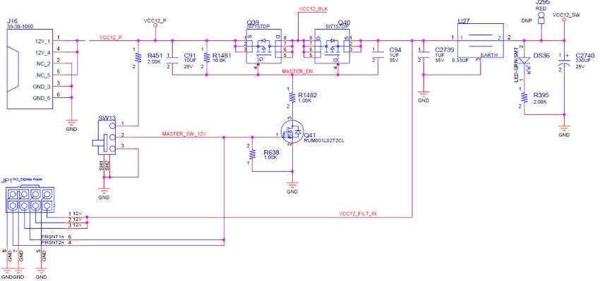
Chapter 1: Introduction
Block Diagram
The VMK180 block diagram is shown in the following figure.
Figure 2: Block Diagram
SysC, GPIO HDMI, PCIe
1.8V 3.3V
GTY0 GTY0 4
HDMI GTY1 GTY HDIO HDIO GTY GTY1
GTY2 GTY2
GTY3 GTY3
Bank 106 Bank 206
HSDP GTY0 GTY0
4
GTY1
GTY2
GTY GTY GTY1
GTY2
2x zSFP GTY3 GTY3
Bank 105 Bank 205
Lane 4 GTY0 GTY0 4
Lane 5
Lane 6
GTY1
GTY2
GTY MIMAC GTY GTY1
GTY2
PCIe Lane 7 GTY3
Bank 104 Bank 204
GTY3
GEN4
x8 Lane 0 GTY0 GTY0 4
Lane 1
Lane 2
GTY1
GTY2
GTY MIMAC GTY GTY1
GTY2
Lane 3 GTY3 GTY3
Bank 103 Bank 203
Versal VM1802 GTY
GTY0
GTY1
4
CPM VSVA2197 Bank 202
GTY2
GTY3
GTY0 4
MIMAC GTY GTY1
GTY2
PMC_MI0[0:25] Bank 500 Bank 201
GTY3
MIO PMC_MI0[26:51] Bank 501 GTY0 4
MIMAC GTY GTY1
GTY2
zQSFP
LP_MI0[0:25] Bank 502 Bank 200
GTY3
XPIO XPIO XPIO XPIO
Triplet 1 Triplet 2 Triplet 3 Triplet 4
700 701 702 703 704 705 706 707 708 709 710 711
DDR4 72-bit LPDDR4 LPDDR4
UDIMM 2x (1x32) 2x (1x32)
FMC+_01 FMC+_02
12
12
X23322-100119
UG1411 (v1.0) January 7, 2021 www.xilinx.com
Send Feedback
VMK180 Board User Guide 8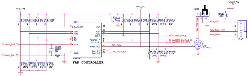
Chapter 1: Introduction

Board Features
       The VMK180 evaluation board features are listed here. Detailed information for each feature is
       provided in Chapter 3: Board Component Descriptions.

       • XCVM1802, VSVA2197 package
       • Form factor: extended height PCIe®, double-slot (heatsink clearance)
       • Onboard configuration from:
          ○   USB-to-JTAG bridge

          ○   JTAG pod 2 mm 2x7 flat cable connector

          ○   microSD card (PS MIO I/F)

          ○   microSD card (System Controller I/F)

       • External boot module (EBM) configuration option
          ○   X-EBM-01 dual quad SPI (QSPI)

       • Clocks
          ○   ACAP Bank 406 HDMI_REC_CLK_OUT 148.50 MHz

          ○   ACAP Bank 503 RTC Xtal 32.768 kHz

          ○   ACAP Bank 503 Si570 REF_CLK 33.3333 MHz

          ○   ACAP Bank 700 Si570 DDR4_CLK (DIMM) 200 MHz

          ○   ACAP Bank 705 Si570 DDR4_CLK2 (LPDDR4) 200 MHz

          ○   ACAP Bank 711 Si570 DDR4_CLK1 (LPDDR4) 200 MHz

          ○   ACAP Bank GTY103/4 (REFCLK0) PCIe_CLK0/1 100 MHz

          ○   ACAP Bank GTY105 (REFCLK0) Si570 zSFP_SI570_CLK 156.250 MHz

          ○   ACAP Bank GTY105 (REFCLK1) Si570 HSDP_SI570_CLK 156.250 MHz

          ○   ACAP Bank GTY200 (REFCLK0) 8A34001_CLK1_IN 100 MHz

          ○   IEEE-1588 eCPRI 8A34001 clocks (various)

       • DDR4 8 GB 72-bit UDIMM
          ○   XPIO triplet 1 (banks 700, 701, 702)

       • Two LPDDR4 interfaces (2x32-bit 4 GB components each)
          ○   XPIO triplets 2 (banks 703, 704, 705) and 4 (banks 709, 710, 711)

UG1411 (v1.0) January 7, 2021                                                            www.xilinx.com
                                                                      Send Feedback
VMK180 Board User Guide                                                                               9
Chapter 1: Introduction

       • PL FMCP HSCP (FMC+) connectivity
          ○   XPIO triplet 3 (banks 706, 707, 708)

          ○   FMCP1 HSCP full LA[00:33] bus

          ○   FMCP2 HSCP full LA[00:33] bus

       • PL GPIO connections
          ○   PL UART1 to FTDI

          ○   PL GPIO DIP switch (4-position)

          ○   PL GPIO pushbuttons (two)

          ○   PL GPIO LEDs (four)

          ○   PL GPIO DC configuration header

          ○   PL SYSCTLR_GPIO[0:5]

       • 44 PL GTY transceivers (11 quads)
          ○   PCIe 8-lane edge connector (8, banks GTY103, GTY104)

          ○   HSDP USB3.1 TYPE C (1, bank GTY105)

          ○   zSFP28 (2, bank GTY105)

          ○   HDMI (3, bank GTY106)

          ○   HDMI TX only, RX not used (1, bank GTY106)

          ○   zQSFP28 (4, bank GTY200)

          ○   FMCP1 HSCP DP (12, banks GTY201-GTY203)

          ○   FMCP2 HSCP DP (12, banks GTY204-GTY206)

          ○   Not used (1, bank GTY105)

       • PCI Express endpoint connectivity
          ○   Gen1 8-lane (x8)

          ○   Gen2 8-lane (x8)

          ○   Gen3 8-lane (x8)

          ○   Gen4 8-lane (x8)

       • PS PMC MIO connectivity
          ○   PS MIO[0:12]: boot configuration header
              - DC QSPI support

UG1411 (v1.0) January 7, 2021                                                          www.xilinx.com
                                                                     Send Feedback
VMK180 Board User Guide                                                                             10
Chapter 1: Introduction
○ PS MIO[13:25]: USB2.0
○ PS MIO[26:36, 50:51]: SD1 I/F
○ PS MIO[37]: ZU4_TRIGGER
○ PS MIO[38:39]: PCIe_WAKE_B, PCIe_PERST_B
○ PS MIO[40:41]: CAN1
○ PS MIO[42:43]: UART0 to FTDI
○ PS MIO[44:47]: I2C1, I2C0
○ PS MIO[48:49], PS LPD MIO[0:25]: dual GEM0/1 RGMII Ethernet with stacked RJ-45
• Security: PSBATT button battery backup
• SYSMON header
• Operational switches (power on/off, PROG_B, boot mode DIP switch)
• Operational status LEDs (INIT, DONE, PS STATUS, PGOOD)
• Power management
• System Controller (XCZU4EG)
The VMK180 provides a rapid prototyping platform using the XCVM1802-2MSEVSVA2197
device. See the Versal Architecture and Product Data Sheet: Overview (DS950) for a feature set
overview, description, and ordering information.
UG1411 (v1.0) January 7, 2021 www.xilinx.com
Send Feedback
VMK180 Board User Guide 11Chapter 1: Introduction
Board Specifications
Dimensions (Extended Height PCIe Form-Factor)
Height: 7.477 inches (18.992 cm)
Length: 9.50 inches (24.13 cm) (¾ PCIe length)
Thickness: 66.87 mil ±10% (1.698 mm ±10%)
Note: Reserve two adjacent PCIe slots to accommodate fan-sink height.
Note: A 3D model of this board is not available.
See the VMK180 evaluation board website for the XDC listing and board schematics.
Environmental
Temperature
Operating: 0°C to +45°C
Storage: -25°C to +60°C
Humidity
10% to 90% non-condensing
Operating Voltage
+12 VDC
UG1411 (v1.0) January 7, 2021 www.xilinx.com
Send Feedback
VMK180 Board User Guide 12Chapter 2: Board Setup and Configuration
Chapter 2
Board Setup and Configuration
Standard ESD Measures
CAUTION! ESD can damage electronic components when they are improperly handled, and can result in
total or intermittent failures. Always follow ESD-prevention procedures when removing and replacing
components.
To prevent ESD damage:
• Attach a wrist strap to an unpainted metal surface of your hardware to prevent electrostatic
discharge from damaging your hardware.
• When you are using a wrist strap, follow all electrical safety procedures. A wrist strap is for
static control. It does not increase or decrease your risk of receiving electric shock when you
are using or working on electrical equipment.
• If you do not have a wrist strap, before you remove the product from ESD packaging and
installing or replacing hardware, touch an unpainted metal surface of the system for a
minimum of five seconds.
• Do not remove the device from the antistatic bag until you are ready to install the device in
the system.
• With the device still in its antistatic bag, touch it to the metal frame of the system.
• Grasp cards and boards by the edges. Avoid touching the components and gold connectors on
the adapter.
• If you need to lay the device down while it is out of the antistatic bag, lay it on the antistatic
bag. Before you pick it up again, touch the antistatic bag and the metal frame of the system at
the same time.
• Handle the devices carefully to prevent permanent damage.
Board Component Location
The following figure shows the VMK180 board component locations. Each numbered component
shown in the figure is keyed to the table in Board Component Descriptions.
UG1411 (v1.0) January 7, 2021 www.xilinx.com
Send Feedback
VMK180 Board User Guide 13Chapter 2: Board Setup and Configuration
IMPORTANT! The following figure is for visual reference only and might not reflect the current revision of
the board.
IMPORTANT! There could be multiple revisions of this board. The specific details concerning the
differences between revisions are not captured in this document. This document is not intended to be a
reference design guide and the information herein should not be used as such. Always refer to the
schematic, layout, and XDC files of the specific VMK180 version of interest for such details.
Figure 3: Evaluation Board Component Locations
Round callout references a component Square callout references a component
00 00
on the front side of the board on the back side of the board
19 17 32
18 20 21
53 16
18 19 30
55 28
54 16 17
49 31
51
7 44
11 35
9 25
45 27
38
3 27
48
10
40
50 52 43
29
4 5
12 1
14
37
6
8 47 46
36
39 24
13
2
33 42
23 41 22
11
34 26
15
X24958-121420
UG1411 (v1.0) January 7, 2021 www.xilinx.com
Send Feedback
VMK180 Board User Guide 14Chapter 2: Board Setup and Configuration
Board Component Descriptions
The following table identifies the components and references the respective schematic
(038-05005-01) page numbers.
CAUTION! Do NOT plug a PC ATX power supply 6-pin connector into the VMK180 board power
connector J16. The ATX 6-pin connector has a different pinout than J16. Connecting an ATX 6-pin
connector into J16 damages the VMK180 board and voids the board warranty.
Table 2: Board Component Locations
Schematic
Callout Ref. Des. Feature Notes
Page
XCVM1802-2MSEVSVA2197
1 U1 Versal™ ACAP The heatsink is not shown in
Figure 31
DDR4 288-pin DIMM SOCKET/ FCI 10124677-000100ILF/Micron
2 J45 43
DDR4 DIMM MTA9ADF1G72AZ-3G2E1
LPDDR4 16 GBIT comp. memory
3 U25,U26 Micron MT53D512M32D2DS-046 27,28
(B710/B711 IF)
LPDDR4 16 GBIT comp. memory
4 U150,U151 Micron MT53D512M32D2DS-046 29, 30
(B709/B710 IF)
Fast-boot module daughter card Samtec SEAF-30-05.0-L-08-1-A-K-
5 J212 31
connector TR
ACAP MODE 4-pole DIP switch,
6 SW1 C&K SDA04H1SBD 12
active-High
ACAP JTAG 2 mm 2x7 flat-cable
7 J36 Molex 87832-1420 24
connector
USB-UART bridge, USB Type-C FTDI FT4232HL-REEL, Amphenol
8 U20,J207 25, 99
connector (USB2.0) 12401598E4#2A
USB ULPI transceiver, USB 2.0 SMSC USB3320C-EZK, WURTH
9 U99,J308 24
type A connector 629104190121
Versal ACAP SD 3.0 level- Nexperia IP4856CX25/CZ, ALPS
10 U104,J302 76
translator circuit, SD card socket SCHA4B0419
11 U33,U35,U214 I2C bus switches TI TCA9548APWR 44, 45
12 U233 I2C bus expander TI TCA6416APWR 55
zSFP/zSFP+ (1x2 stacked)
13 J287 Tyco 2198318-6 45
connector
14 J288 zQSFPConnector TE 1551920-2 47
PCIe EndPoint 8-lane edge
15 P3 NA - PCB layout feature 46
connector
GEM0 SGMII Ethernet PHY, TI DP83867ISRGZ, TE-AMP
16 U198,J307B(UPR) 77
0x01, RJ45 w/mag 2301997-7 dual port
GEM1 SGMII Ethernet PHY, TI DP83867ISRGZ, TE-AMP
17 U134,J307A(LWR) 78
0x02, RJ45 w/mag 2301997-7 dual port
HDMI XMT, TMDS to HDMI level TI SN65DP159RGZ, TE 1888811-1
18 U43,P2A(UPR) 50
shifter retimer, 0x22, 0xBC dual port
HDMI RCV TMDS retimer, 0x0B, TI TMDS181IRGZT, TE 1888811-1
19 U55,P2B(LWR) 51
0xB8 dual port
UG1411 (v1.0) January 7, 2021 www.xilinx.com
Send Feedback
VMK180 Board User Guide 15Chapter 2: Board Setup and Configuration
Table 2: Board Component Locations (cont'd)
Schematic
Callout Ref. Des. Feature Notes
Page
20 J51 FMCP1 Samtec ASP-184329-01 32-36
21 J53 FMCP2 Samtec ASP-184329-01 37-41
User LEDs and 4-pole DIP Lumex SML-LX0603GW (green),
22 DS3-DS6,SW6 53
switch, active-High C&K SDA04H1SBD
23 SW4,SW5 User pushbutton, active-High E-switch TL3301EP100QG 53
24 U216,J309 SPDIF IF driver and RCA jack TI SN74AVC1T45, CUI RCJ-021 79
CAN BUS transceiver, 2x4 CAN Nexperia TJA1057GT/3J, SULLINS
25 U110,J5 80
header PBC04DAAN
SYSMON 2X6 vertical male pin
26 J11 SULLINS PBC06DAAN 12
header
Power management system
27 Various Infineon regulators 47-60
(top, [bottom])
28 J325 PMBus 3-pin header SULLINS PBC03SAAN 26
Lumex SML-LX0603GW-TR,
29 DS9-DS17,DS19-DS32 Power good LEDs 83
green
30 SW13 Power On/Off slide switch C&K 1201M2S3AQE2 46
Power connector, 2x3, for AC-DC
31 J16 MOLEX 39-30-1060 (mini-fit) 46
power adapter
Power connector, 2x4, for ATX
32 JP1 Astron 6652208-T0003T-H-A 46
PCIe power
33 U64 Fan controller Maxim MAX6643LBBAEE++ 54
34 J233 Fan header (keyed 4-pin) Molex 22-11-2032 54
Power-on reset (POR) with TI TPS389001DSER, E-switch
U10,SW2 15
pushbutton TL3301EP100QG
Alternate POR source driver and TI SN74LVC07A, SULLINS
U110,J326 15
2x4 select header PBC04DAAN
35
GEM0 Ethernet PHY reset
SW15 E-switch TL3301EP100QG 77
pushbutton, active-Low
GEM1 Ethernet PHY reset
SW7 E-switch TL3301EP100QG 78
pushbutton, active-Low
DDR4 DIMM CLK, 200 MHz, 3.3V
36 U2 Silicon Labs SI570BAB000299DG 4
LVDS, 0x60
LPDDR4 CLK2, 200 MHz, 3.3V
37 U3 Silicon Labs SI570BAB000299DG 5
LVDS, 0x60
LPDDR4 CLK1, 200 MHz, 3.3V
38 U4 Silicon Labs SI570BAB000299DG 7
LVDS, 0x60
HSDP CLK, 156.25 MHz, 3.3V
39 U5 Silicon Labs SI570BAB000544DG 8
LVDS, 0x5D
ACAP U1 REF CLK, 33.33 MHz,
40 U32 Silicon Labs SI570JAC000900DG 43
1.8V CMOS, 0x5D
PCIe 1:2 buffer, 100 MHz, 3.3V
41 U39 IDT 85411AMLF 49
LVDS
HDMI jitter atten., 148.50 MHz,
42 U62 IDT 8T49N241-994NLGI 52
3.3V LVDS, 0x6C
UG1411 (v1.0) January 7, 2021 www.xilinx.com
Send Feedback
VMK180 Board User Guide 16Chapter 2: Board Setup and Configuration
Table 2: Board Component Locations (cont'd)
Schematic
Callout Ref. Des. Feature Notes
Page
SYSCTLR clocks 33.33 MHz & 125 Silicon Labs Si5332FD10259-
43 U142 101
MHz I2C 0x6A GM1
zSFP CLK, 156.25 MHz, 3.3V
44 U192 Silicon Labs SI570BAB000544DG 8
LVDS, 0x5D
IEEE-1588 eCPRI input CLK, 100
45 U205 Silicon Labs SI570BAC002038DG 48
MHz, 3.3V LVDS, 0x5F
IEEE-1588 eCPRI CLK, various,
46 U219 IDT 8A34001E-000AJG8 104
3.3V, 0x58
IEEE-1588 eCPRI 8A34001 CLK in
47 J328-J331 Rosenberger 32K10K-400L5 104
and out SMA pairs
48 U125 XCZU4EG System Controller TI MSP430F5342 85-91
System Controller MODE 4-pole
49 SW11 C&K SDA04H1SBD 89
DIP switch, active-High
System Controller JTAG 2 mm 2
50 J202 Molex 87832-1420 89
x 7 flat-cable connector
System Controller SD card
51 J206 ALPS SCHA4B0419 96
socket
System Controller LPDDR4 16
52 U132 Micron MT53D512M32D2DS-046 97
GBIT comp. memory
System Controller SGMII Marvell 88E1512-A0-NNP2C000,
53 U131,J204 95
Ethernet, RJ45 w/magnetics Halo HFJ11-1G01E-L12RL
System Controller pushbutton
54 SW16 E-switch TL3301EP100QG 88
switch, active-High
System Controller POR with TI TPS389001DSER, E-switch
55 U129,SW12 88
pushbutton TL3301EP100QG
Notes:
1. The VMK180 evaluation board includes a Cofan USA 30-6156-06 heatsink with a thermal resistance of 0.27°C/W.
Default Jumper and Switch Settings
The following figure shows the VMK180 board jumper header and switch locations. Each
numbered component shown in the figure is keyed to the applicable table in this section. Both
tables reference the respective schematic page numbers.
UG1411 (v1.0) January 7, 2021 www.xilinx.com
Send Feedback
VMK180 Board User Guide 17Chapter 2: Board Setup and Configuration
Figure 4: Board Jumper Header and Switch Locations
11
16
6 14
8
2 12
9
13
4
3
15
10
5
7
1
X23150-121420
Jumpers
The following table lists the default jumper settings.
Table 3: Default Jumper Settings
Callout Schematic
Ref. Des. Function Default
Number Page
SYSMON VREFP
1 J12 1-2: 1.024V VREFP connected to ACAP 1-2 12
2-3: VREFP connected to GND
UG1411 (v1.0) January 7, 2021 www.xilinx.com
Send Feedback
VMK180 Board User Guide 18Chapter 2: Board Setup and Configuration
Table 3: Default Jumper Settings (cont'd)
Callout Schematic
Ref. Des. Function Default
Number Page
POR_B sense select
2 J26 1-2: VCCO_503 1-2 15
2-3: VCCAUX_PMC
SFP1_TX_DISABLE select
3 J32 ON: enable always ON 45
OFF: disable/allows ACAP U1 control
ACAP U1 bank VCC_FUSE select
4 J34 1-2: VCC1V8 2-3 17
2-3: GND
SFP0_TX_DISABLE select
5 J35 ON: enable always ON 17
OFF: disable/allows ACAP U1 control
JTAG MUX U14/U15 OE_B
6 J37 1-2: UTIL_3V3 disable 2-3 24
2-3: GND enable
PCIe lane size select
1-2: x1
7 J60 5-6 46
3-4: x4
5-6: x8
SYSCTLR_POR_B enable
8 J203 ON: enable ON 89
OFF: disable
System Controller M88E1512 EPHY U131 configuration
1:2: GND (5'b00000)
9 J205 3:4: SYSCTLR_ETH_LED0 7-8 95
5:6: SYSCTLR_ETH_LED0
7:8: SYS_VCC1V8 (5'b00001)
ACAP cooling fan control
10 J234 1-2: MAX6643 U64 control is enabled 2-3 54
2-3: always on
ULPI USB3320 U99 USB conn. J308 shield select
8 J300 1-2: J308 shield directly to GND 1-2 42
2-3: J308 shield capacitor C2762 to GND
IP4856 U104 VERSAL_SD1_REF voltage select
8 J301 1-2: UTIL_3V3 1-2 76
2-3: GND
UG1411 (v1.0) January 7, 2021 www.xilinx.com
Send Feedback
VMK180 Board User Guide 19Chapter 2: Board Setup and Configuration
Table 3: Default Jumper Settings (cont'd)
Callout Schematic
Ref. Des. Function Default
Number Page
Si53340 clock MUX U206 input select
11 J306 ON: CLK1 8a34001_Q2 OFF 48
OFF: U205 USER_SI570_1(100 MHz default)
POR_B source select (OR’d with POR_B)
None: U10 TPS389001 POR only
1-2
1-2: U125 SYSCTLR_POR_B
12 J326 3-4 15
3-4: J36 PC4_POR_B
7-8
5-6: J212(B) DC_PS_POR_B_OUT
7-8: U20 FTDI_POR_B
Switches
The following table lists the default switch settings.
Table 4: Default Switch Settings
Callout Schematic
Ref. Des. Function Default
Number Page
13 SW1 ACAP U1 mode 4-pole DIP switch 0000 14
Switch OFF = 1 = High; ON = 0 = Low
Mode = SW1[4:1] = Mode[3:0]
JTAG = ON,ON,ON,ON = 0000
QSPI32 = ON,ON,OFF,ON = 0010
SD = OFF,OFF,OFF,ON = 1110
Reserved for Xilinx® = OFF,OFF,OFF,OFF = 1111
JTAG MUX select 2-pole DIP switch
Switch OFF = 1 = High; ON = 0 = Low
14 SW3 SW3[1:2] = MUX[S0:S1] 01 24
SYSCTLR U125 BANK 44 = ON,ON = 00
FTDI BRIDGE U20 = ON,OFF = 01
ACAP U1 BANK 306 GPIO 4-Pole DIP switch
15 SW6 SW6[4:1] = GPIO_DIP_SW[0:3] 0000 53
Switch OFF = 0 = Low; ON = 1 = High
ZU4 SYSCTLR U125 Mode 4-Pole DIP switch
Switch OFF = 1 = High; ON = 0 = Low
Mode = SW11[4:1] = Mode[3:0]
16 SW11 0000 89
JTAG = ON,ON,ON,ON = 0000
QSPI32 = ON,ON,OFF,ON = 0010
SD = OFF,OFF,OFF,ON = 1110
UG1411 (v1.0) January 7, 2021 www.xilinx.com
Send Feedback
VMK180 Board User Guide 20Chapter 2: Board Setup and Configuration
Versal ACAP Configuration
The Versal XCVM1802 ACAP boot process is described in the “Platform Boot, Control, and
Status” section of the Versal ACAP Technical Reference Manual (AM011). The VMK180 board
supports a subset of the modes documented in the technical reference manual via onboard and
daughter card boot options. The mode DIP switch SW1 configuration option settings are listed in
the following table.
Table 5: Mode Switch SW1 Configuration Option Settings
Mode Pins
Boot Mode Mode SW1 [4:1]2 Comments
[3:0]2
JTAG 00001, 3 ON, ON, ON, ON Supported with or without boot module attached
Supported only with boot module X-EBM-01 attached
QSPI32 0010 ON, ON, OFF, ON
Supports x1, x2, x4, and dual-parallel x8
SD1_3.0 1110 OFF, OFF, OFF, ON Supported with or without boot module attached
Notes:
1. Default switch setting.
2. Mode DIP SW1 poles [4:1] correspond to U1 XCVM1802 MODE[3:0].
3. Mode DIP SW1 individual switches ON=LOW (p/d to GND)=0, OFF=HIGH (p/u to VCCO)=1.
JTAG
The Vivado®, XilinxSDK, or third-party tools can establish a JTAG connection to the Versal ACAP
in the two ways described here:
• FTDI FT4232 USB-to-JTAG/USB-UART device (U20) connected to USB 3.1 type-C connector
(J207), which requires:
○ Set boot mode SW1 for JTAG as indicated in the "Mode Switch SW1 Configuration Option
Settings" table in Versal ACAP Configuration
○ Set 2-pole DIP SW3[1:2] set to 01 (ON, OFF) for JTAG MUX channel 2 FT4232 U20 bridge
○ On the 3-pin JTAG MUX, enable header J37 (2-pin jumper block installed on pins 2-3) to
enable the JTAG MUX
○ Power-cycle the VMK180 board or press the power-on reset (POR) pushbutton (SW2)
(SW2 is callout 46 in the "Evaluation Board Component Locations" figure in Board
Component Location)
• JTAG pod flat cable connector J36 (2 mm 2x7 shrouded/keyed), which requires:
○ Set boot mode SW1 for JTAG as indicated in the "Mode Switch SW1 Configuration Option
Settings" table in Versal ACAP Configuration
○ On the 3-pin JTAG MUX, enable header J37 (2-pin jumper block installed on pins 1-2) to
inhibit the JTAG MUX (hi-Z mode)
UG1411 (v1.0) January 7, 2021 www.xilinx.com
Send Feedback
VMK180 Board User Guide 21Chapter 2: Board Setup and Configuration
○ 2-pole DIP SW3[1:2] setting is XX as the MUX is inhibited/turned off
○ In this mode, the FT4232 device (U20) UART functionality continues to be available
○ Power-cycle the VMK180 board or press the power-on reset pushbutton (SW2) (SW2 is
callout 46 in the "Evaluation Board Component Locations" figure in Board Component
Location)
QSPI32
This boot mode is supported only with boot module X-EBM-01 attached to the MIO connector
(J212). J212 is a 240-pin (8 x 30) MIO connector wired to XCVM1802 U1 bank 500
PMC_MIO[0:12] pins. The supported QSPI configurations are x1, x2, x4, and dual-parallel x8. To
boot from a QSPI X-EBM-01 boot module:
1. Store a valid XCVM1802 ACAP boot image file on the X-EBM-01 resident QSPI.
2. Set boot mode SW1 for QSPI32 as indicated in the "Mode Switch SW1 Configuration Option
Settings" table in Versal ACAP Configuration.
3. Power-cycle the VMK180 or press the POR pushbutton SW2. SW2 is callout 35 in the
"Evaluation Board Component Locations" figure in Board Component Location.
SD1_3.0
To boot from a SD card installed in microSD card socket J302:
1. Store a valid XCVM1802 ACAP boot image file on a microSD card. Plug the SD card into the
VMK180 board SD socket J302 connected to the XCVM1802 U1 bank 501 MIO SD
interface.
2. Set boot MODE SW1 for SD1_3.0 as indicated in the "Mode Switch SW1 Configuration
Option Settings" table in Versal ACAP Configuration.
3. Power-cycle the VMK180 or press the POR pushbutton SW2. SW2 is callout 35 in the
"Evaluation Board Component Locations" figure in Board Component Location.
UG1411 (v1.0) January 7, 2021 www.xilinx.com
Send Feedback
VMK180 Board User Guide 22Chapter 3: Board Component Descriptions
Chapter 3
Board Component Descriptions
Overview
This chapter provides a detailed functional description of the board’s components and features.
The "Board Component Locations" table in Board Component Descriptions identifies the
components and references the respective schematic page numbers. Component locations are
shown in the "Evaluation Board Component Locations" figure in Board Component Location.
Component Descriptions
Versal ACAP
[Figure 3, callout 1]
The VMK180 board is populated with the Versal™ XCVM1802-2MSEVSVA2197 ACAP, which
combines a powerful processing system (PS) and programmable logic (PL) in the same device. The
PS in a Versal ACAP features the Arm® flagship Cortex™-A72 64-bit dual-core processor and
Cortex™-R5F dual-core real-time processor. For additional information on the Versal
XCVM1802-2MSEVSVA2197 ACAP, see the Versal Prime Series Data Sheet: DC and AC Switching
Characteristics (DS956). See the Versal ACAP Technical Reference Manual (AM011) for more
information about Versal ACAP configuration options.
Encryption Key Battery Backup Circuit
The XCVM1802 ACAP U1 implements bitstream encryption key technology. The VMK180 board
provides the encryption key backup battery circuit shown in the following figure.
UG1411 (v1.0) January 7, 2021 www.xilinx.com
Send Feedback
VMK180 Board User Guide 23Chapter 3: Board Component Descriptions
Figure 5: Encryption Key Backup Circuit
X23376-112420
The Seiko TS621E rechargeable 1.5V lithium button-type battery B1 is soldered to the board
with the positive output connected to the XCVM1802 ACAP U1 VCC_BATT bank pin AG33. The
battery supply current IBATT specification is 150 nA maximum when board power is off. Battery
B1 is charged from the VCC1V8 1.8V rail through a 2 series diode with the first forward drop to
yield between 0.24V to 0.46V over temperature per fixed 5 mA load, R1725, and limiting 1.56V
max at the ACAP pin, PSVBATT. The second diode and 4.7 kΩ current limit resistor allows the
battery to trickle charge and prevent battery B1 from back powering R1725.
I/O Voltage Rails
The XCVM1802 ACAP PL I/O bank voltages on the VMK180 board are listed in the following
table.
Note: The VMK180 board is shipped with VADJ_FMC set to 1.5V by the ZU4 system controller.
Table 6: I/O Voltage Rails
ACAP (U1) Power Supply Rail
Voltage Description
Bank Net Name
HDIO Bank 306 VCC1V8 1.8V GPIO: PB[0:1], DIP_SW[0:3], LED[0:3]; DC_PL_GPIO[0:3];
SYSCTLR_GPIO[0:5]; UART1_TXD/RXD
HDIO Bank 406 VCC3V3 3.3V HDMI status/ctrl(15)IF; HDIO_UART3_TX/RX;
HDIO_UART4_TX/RX
XPIO Bank 700 VCC1V2_DDR4 1.2V DDR4_DIMM1_DQ[32:63], CB[0:7], ADDR/CTRL;
DDR4_DIMM1_CLK; Si570 U2 200 MHz
XPIO Bank 701 VCC1V2_DDR4 1.2V DDR4_DIMM1_DQ[24:31], ADDR/CTRL
XPIO Bank 702 VCC1V2_DDR4 1.2V DDR4_DIMM1_DQ[0:23], CB[0:7]
UG1411 (v1.0) January 7, 2021 www.xilinx.com
Send Feedback
VMK180 Board User Guide 24Chapter 3: Board Component Descriptions
Table 6: I/O Voltage Rails (cont'd)
ACAP (U1) Power Supply Rail
Voltage Description
Bank Net Name
XPIO Bank 703 VCC1V1_LP4 1.1V LPDDR4_3_DQ[0:7, 16:23], ADDR/CTRL
XPIO Bank 704 VCC1V1_LP4 1.1V LPDDR4_2_DQ[0:7, 16:23]; LPDDR4_3_DQ[8:15, 24:31]
XPIO Bank 705 VCC1V1_LP4 1.1V LPDDR4_2_DQ[8:15, 24:31], ADDR/CTRL; Si570 U3 200 MHz
XPIO Bank 706 VADJ_FMC 1.5V 8A34001_GPIO_[0:15]; FMCP1_LA[00:16]
XPIO Bank 707 VADJ_FMC 1.5V FMCP1_LA[17:33]; FMCP2_LA[26:33]
XPIO Bank 708 VADJ_FMC 1.5V FMCP2_LA[00:25]
XPIO Bank 709 VCC1V1_LP4 1.1V LPDDR4_1_DQ[0:7, 16:23], ADDR/CTRL
XPIO Bank 710 VCC1V1_LP4 1.1V LPDDR4_0_DQ[0:7, 16:23]; LPDDR4_1_DQ[8:15, 24:31]
XPIO Bank 711 VCC1V1_LP4 1.1V LPDDR4_0_DQ[8:15, 24:31], ADDR/CTRL; Si570 U4 200 MHz
PMC MIO 500 VCCO_500 3.3V SYSMON IF; PMC_MIO[0:25]_500; ISL60002 U6 1.042V VREF;
J1 2x6 SYSMON PIN HDR
PMC MIO 501 VCCO_501 3.3V PMC_MIO[26:51]
LP MIO 502 VCCO_502 3.3V LPD_MIO[0:25]
DDR4 UDIMM Socket
[Figure 3, callout 1]
The VMK180 board XPIO triplet 1 (banks 700/701/702) memory interface supports 288-pin 72-
bit DDR4 DIMM socket J45.
Figure 6: DDR4 DIMM Memory
XPIO
Triplet 1
700 701 702
DDR4 72-bit
UDIMM
X23197-120120
The VMK180 board is shipped with a DDR4 UDIMM installed:
• Manufacturer: Micron
UG1411 (v1.0) January 7, 2021 www.xilinx.com
Send Feedback
VMK180 Board User Guide 25Chapter 3: Board Component Descriptions
• Part number: MTA9ADF1G72AZ-3G2E1
• Description
○ 8 GB 288-pin DDR UDIMM
○ Single rank
○ 8 Gb (1 Gig x 8), 16 banks
○ Supports up to 3200 Mb/s
The VMK180 XCVM1802 ACAP DDR interface performance is documented in the Versal Prime
Series Data Sheet: DC and AC Switching Characteristics (DS956). The VMK180 DDR4 DIMM
interface adheres to the constraints guidelines documented in the PCB guidelines for DDR4
section of the Versal ACAP PCB Design User Guide (UG863). The DDR4 DIMM interface is a 40Ω
impedance implementation. Other memory interface details are also available in the Versal ACAP
Memory Resources Architecture Manual (AM007). For more details, see the Micron
MTA9ADF1G72AZ-3GE1 data sheet at the Micron website. The ACAP connections for the
feature described in this section are documented in the VMK180 board XDC file, referenced in
Appendix B: Xilinx Design Constraints.
LPDDR4 Component Memory
[Figure 3, callout 3 and 4]
The VMK180 board hosts two LPDDR4 memory systems, each with a component configuration
of 2x (1x32-bit component).
Figure 7: LPDDR4 Component Memory
XPIO XPIO XPIO
Triplet 2 Triplet 3 Triplet 4
703 704 705 706 707 708 709 710 711
LPDDR4 LPDDR4
2x (1x32) 2x (1x32)
X23198-090919
XCVM1802 U1 XPIO triplet 2 (banks 703/704/704) and triplet 4 (banks 709/710/711) each
support two independent 32-bit 2 GB component interfaces (4 GB per triplet).
• Manufacturer: Micron
UG1411 (v1.0) January 7, 2021 www.xilinx.com
Send Feedback
VMK180 Board User Guide 26Chapter 3: Board Component Descriptions
• Part number: MT53D512M32D2DS-046 WT:D (dual die LPDDR4 SRAM)
• Component description
○ 16 Gb (512 Mb x 32)
○ 1.1V 200-ball WFBGA
○ DDR4-2133
The VMK180 XCVM1802 ACAP PL DDR interface performance is documented in the Versal
Prime Series Data Sheet: DC and AC Switching Characteristics (DS956). The VMK180 board
LPDDR4 component memory interfaces adhere to the constraints guidelines documented in the
PCB guidelines for DDR4 section of Versal ACAP PCB Design User Guide (UG863). The VMK180
DDR4 component interface is a 40Ω impedance implementation. Other memory interface details
are also available in the Versal ACAP Memory Resources Architecture Manual (AM007). For more
memory component details, see the Micron MT53D512M32D2DS data sheet at the Micron
website. The detailed ACAP connections for the feature described in this section are
documented in the VMK180 board XDC file, referenced in Appendix B: Xilinx Design
Constraints.
System Reset POR_B
[Figure 3, callout 35]
POR_B is the Versal ACAP processor reset, which can be controlled by:
• SYSCTLR (U125)
• PC4 header (J36)
• MIO EBM (external boot module on J212)
• FTDI USB JTAG chip (U20)
In the following figure, U235 allows directional open drain level shifting for all of these masters,
and J326 allows them to be bused together if desired. The fifth channel buffers POR_B out to
the EBM (external boot module) as DC_PS_POR_B. The TPS389001 U10 supervisor chip holds
POR_B off until power is valid. The VMK180 board POR circuit is shown in the figure.
UG1411 (v1.0) January 7, 2021 www.xilinx.com
Send Feedback
VMK180 Board User Guide 27Chapter 3: Board Component Descriptions
Figure 8: POR_B Reset Circuit
X24949-121420
PMC and LPD MIO
The following table provides MIO peripheral mapping implemented on the VMK180 board. See
the Versal ACAP Technical Reference Manual (AM011) for more information on MIO peripheral
mapping. The XCVM1802 ACAP Bank 500, 501, and 502 mappings are listed in the table.
Table 7: MIO Peripheral Mapping
PMC MIO[0:25] Bank 500 PMC MIO[26:51] Bank 501 LPD MIO[0:25] Bank 502
0 MIO CONN. J212 26 SD1 0 GEM0
1 MIO CONN. J212 27 SD1 1 GEM0
2 MIO CONN. J212 28 SD1 2 GEM0
3 MIO CONN. J212 29 SD1 3 GEM0
4 MIO CONN. J212 30 SD1 4 GEM0
5 MIO CONN. J212 31 SD1 5 GEM0
6 MIO CONN. J212 32 SD1 6 GEM0
7 MIO CONN. J212 33 SD1 7 GEM0
8 MIO CONN. J212 34 SD1 8 GEM0
9 MIO CONN. J212 35 SD1 9 GEM0
10 MIO CONN. J212 36 SD1 10 GEM0
11 MIO CONN. J212 37 ZU4_TRIGGER 11 GEM0
12 MIO CONN. J212 38 PCIE_PERST_B 12 GEM1
13 U103.6 USB3320 U99 reset gate 39 PCIE_PWRBRK_B 13 GEM1
14 USB3320 U99 40 CAN1_TXD 14 GEM1
15 USB3320 U99 41 CAN1_RXD 15 GEM1
16 USB3320 U99 42 UART0 16 GEM1
17 USB3320 U99 43 UART0 17 GEM1
18 USB3320 U99 44 I2C1 18 GEM1
UG1411 (v1.0) January 7, 2021 www.xilinx.com
Send Feedback
VMK180 Board User Guide 28Chapter 3: Board Component Descriptions
Table 7: MIO Peripheral Mapping (cont'd)
PMC MIO[0:25] Bank 500 PMC MIO[26:51] Bank 501 LPD MIO[0:25] Bank 502
19 USB3320 U99 45 I2C1 19 GEM1
20 USB3320 U99 46 I2C0 20 GEM1
21 USB3320 U99 47 I2C0 21 GEM1
22 USB3320 U99 48 GEM0 22 GEM1
23 USB3320 U99 49 GEM1 23 GEM1
24 USB3320 U99 50 PCIE_WAKE_B 24 GEM0, GEM1
25 USB3320 U99 51 SD1 25 GEM0, GEM1
PMC MIO[0–12] Bank 500: MIO Daughter Card (DC)
Connector J212
[Figure 3, callout 5]
The VMK180 U1 XCVM1802 bank 500 PMC_MIO[0:12] pins are connected to the 240-pin (8 x
30) MIO connector J212. This interface enables high-speed XCVM1802 configuration using the
X-EBM-01 QSPI external daughter card installed on J212.
The detailed ACAP connections for the feature described in this section are documented in the
VMK180 board XDC file, referenced in Appendix B: Xilinx Design Constraints. The XCVM1802
MIO connector J212 pinout is listed in the following figure.
UG1411 (v1.0) January 7, 2021 www.xilinx.com
Send Feedback
VMK180 Board User Guide 29Chapter 3: Board Component Descriptions
Figure 9: MIO Connector J212 Pinout
VMK180 Config Daughter Cards
X23354-101619
PMC MIO[13:25] Bank 500: USB 2.0 ULPI PHY
The VMK180 board uses a Standard Microsystems Corporation USB3320 USB 2.0 ULPI
transceiver (U99) to support a USB 2.0 type-A connector (J308). A USB cable is supplied in the
VMK180 evaluation kit (standard-A connector to host computer, USB 2.0 A connector to
VMK180 board connector J308). The USB3320 is a high-speed USB 2.0 PHY supporting the
UTMI+ low pin interface (ULPI) interface standard. The ULPI standard defines the interface
between the USB controller IP and the PHY device, which drives the physical USB bus. Using the
ULPI standard reduces the interface pin count between the USB controller IP and the PHY
device.
UG1411 (v1.0) January 7, 2021 www.xilinx.com
Send Feedback
VMK180 Board User Guide 30Chapter 3: Board Component Descriptions
The USB3320 is clocked by a 24 MHz crystal (X8). See the Standard Microsystems Corporation
(SMSC) USB3320 data sheet for clocking mode details. The interface to the USB3320 PHY is
implemented through the IP in the XCVM1802 ACAP PS.
The USB3320 ULPI transceiver circuit has a Micrel MIC2544 high-side programmable current
limit switch (U100). This switch has an open-drain output fault flag on pin 2, which turns on red
LED DS37 if over current or thermal shutdown conditions are detected. DS37 is located just
above the U125 system controller component (callout 48 in the figure in Board Component
Location).
Note: As shown in the following figure, the shield for the USB 2.0 type-A connector (J308) can be tied to
GND by a jumper on header J300 pins 1-2 (default). The USB shield can optionally be connected through a
series capacitor to GND by installing a capacitor (body size 0402) at location C2762 and jumping pins 2-3
on header J300.
Figure 10: USB3320 USB2.0 Connector J308 Shield Connection Options
X24950-121420
The detailed ACAP connections for the feature described in this section are documented in the
VMK180 board XDC file, referenced in Appendix B: Xilinx Design Constraints.
PMC MIO[26:36, 51] Bank 501: Secure Digital (SD)
Card IF (J302)
[Figure 3, callout 10]
UG1411 (v1.0) January 7, 2021 www.xilinx.com
Send Feedback
VMK180 Board User Guide 31Chapter 3: Board Component Descriptions
A secure digital (SD) card connector is provided for booting and file system storage. This
interface is used for the SD boot mode and supports SD2.0 and SD3.0 access.
The SDIO interface signals PMC_MIO[26:36, 51] are connected to XCVM1802 ACAP bank 501,
which has its VCCO set to 3.3V. Six SD interface nets PMC_MIO[26, 29, 30:33] are passed
through a Nexperia IP4856CX25 SD 3.0-compliant voltage level-translator U104 (mounted on an
Aries adapter), present between the XCVM1802 ACAP and the SD card connector (J302). The
Nexperia IP4856CX25 U104 device provides SD3.0 capability with SDR104 performance. The
Aries adapter schematic pinout to IP4856CX25 device pinout cross-reference table is shown in
the following table and also on the VMK180 schematic page for this circuit.
The Nexperia SD3.0 level shifter is mounted on an Aries adapter board (located on the bottom of
the board under SD socket J302) that has the pin mapping shown in the table.
Table 8: IP4856CX25 U104 Adapter Pinout
Aries Adapter Pin Number IP4856CX25 Pin Number IP4856CX25 Pin Name
1 C1 CLK_IN
2 C3 GND
3 D3 CD
4 D2 CMD_H
5 E2 CLK_FB
6 E4 WP
7 B4 VLDO
8 C4 VSD_REF
9 A3 DIR_0
10 A4 VSUPPLY
11 B3 VCCA
12 A2 DIR_CMD
13 D1 DATA0_H
14 B2 SEL
15 B1 DATA3_H
16 E1 DATA1_H
17 E3 DIR_1_3
18 A1 DATA2_H
19 E5 DATA1_SD
20 D5 DATA0_SD
21 C5 CLK_SD
22 D4 CMD_SD
23 B5 DATA3_SD
24 A5 DATA2_SD
25 C2 ENABLE
UG1411 (v1.0) January 7, 2021 www.xilinx.com
Send Feedback
VMK180 Board User Guide 32Chapter 3: Board Component Descriptions
Figure 11: SD Socket J302 Power Control
X24951-121420
Information for the SD I/O card specification can be found at the SanDisk Corporation or SD
Association websites. The VMK180 SD card interface supports the SD1 (2.0) and SD2 (3.0)
configuration boot modes documented in the Versal ACAP Technical Reference Manual (AM011).
For Nexperia IP4856CX25 component details, see the IP4856CX25 data sheet at the Nexperia
website.
The detailed ACAP connections for the feature described in this section are documented in the
VMK180 board XDC file, referenced in Appendix B: Xilinx Design Constraints.
PS MIO[37] ZU4 System Controller GPIO
The ACAP PS bank 501 MIO37 is connected to the ZU4 system controller U125 bank 500
MIO11 pin AE17.
PMC MIO[38:39] PCIe Status
The ACAP PS bank 501 MIO38 (PCIE_PERST_B) and MIO50 (PCIE_WAKE_B) are connected to
the PCIe 8-lane edge connector P3 PERST# (pin A11) and WAKE# (pin B11), respectively.
PMC MIO[40:41] CAN1
[Figure 3, callout 25]
UG1411 (v1.0) January 7, 2021 www.xilinx.com
Send Feedback
VMK180 Board User Guide 33Chapter 3: Board Component Descriptions
The ACAP PS bank 501 MIO40 (TX OUT) and MIO41 (RX IN) support the PS-side CAN bus TX
and RX interface wired through the TI SN74AVC2T244 level-translators U107 and U109,
respectively, to the NXP TJA1057GT/3J CAN-bus transceiver U110. This transceiver is
connected to the 2x4 0.1-inch pitch 8-pin male header J5.
See the NXP TJA1057GT/3J data sheet at the Nexperia website for CAN-bus transceiver details.
The detailed ACAP connections for the feature described in this section are documented in the
VMK180 board XDC file, referenced in Appendix B: Xilinx Design Constraints.
PMC MIO[42:43] UART0
[Figure 3, callout 8]
This is the primary Versal ACAP PS-side UART interface. The VMK180 USB Type-C connector
J207 only supports USB2.0.
MIO42 (RX_IN) and MIO43 (TX_OUT) are connected to FTDI FT4232HL U20 USB-to-Quad-
UART bridge port BD through TI SN74AVC4T245 level-shifters U18 and U21. The FT4232HL
U20 port assignments are listed in the following table.
Table 9: FT4232HL Port Assignments
FT4232HL U34 Versal ACAP U1
Port AD JTAG VMK180 JTAG chain
Port BD UART0 PS_UART0 (MIO 18-19)
Port CD UART1 PL_UART1 bank 306
Port DD UART2 U20 system controller UART
The FT4232HL UART interface connections are shown in the following figure.
UG1411 (v1.0) January 7, 2021 www.xilinx.com
Send Feedback
VMK180 Board User Guide 34Chapter 3: Board Component Descriptions
Figure 12: FT4232HL UART Connections
PC4
HDR
FMC+ FMC+
USB
Type-C
xxxx
xxxx
xx
xx
FTDI XCVM1802
xxxx
xxxx
xx
xx
ACAP
xxxx
xxxx
xx
xx
TDO
Versal JTAG
xxxx
xxxx
PortA TDI
xx
xx
USB2.0 Versal PS UART
PortB PS UART GTY
xxxx
xxxx
xx
xx
Versal PS UART
PortC PL UART HSDP
xxxx
xxxx
xx
xx
PortD SysCon UART
xxxx
xxxx
xx
xx
xxxx
xxxx
xx
xx
xxxx
xxxx
xx
xx
xxxx
xxxx
xx
xx
ZU4
xxxx
xxxx
xx
xx
MPSoC JTAG PC4
xxxx
xxxx
xx
xx
HDR
HSDP Using
USB3.0 Pins
PS UART
Note:
1. No USB3.0 support.
X23334-100719
For more information on the FT4232HL, see the Future Technology Devices International Ltd
website.
The detailed ACAP connections for the feature described in this section are documented in the
VMK180 board XDC file, referenced in Appendix B: Xilinx Design Constraints.
PMC MIO[46:47] I2C0, PMC MIO[44:45] I2C1 I2C Bus
Overview
The following figure shows an overview of the I2C0 and I2C1 bus connections.
UG1411 (v1.0) January 7, 2021 www.xilinx.com
Send Feedback
VMK180 Board User Guide 35Chapter 3: Board Component Descriptions
Figure 13: I2C0 and I2C1 Bus Connectivity Overview
I2C0 I2C1
0x74 0 DC_I2C
System Controller 1 FMCP1_IIC
U212 U213
L/S PS Bank 501 L/S 2 FMCP2_IIC
U125 XCZU4EG I2C 3 DDR4_DIMM1
MUX 4 LPDDR4_SI570_CLK2
Versal ACAP #1
U210 U211 5 LPDDR4_SI570_CLK1
L/S PS Bank 501 L/S 6 HSDP_SI570
U1 7 8A34001
U35 TCA9548A
0x20 P00 MAX6643_OT_B
P01 MAX6643_FANFAIL_B 0x75 0 SFP0_IIC
P04 PMBUS2_INA226_ALERT 1 SFP1_IIC
P07 MAX6643_FULLSPD 2 QSFP1_I2C
I2C
MUX 3 NC
P10 FMCP1_FMC_PRSNT_M2C_B #2 4 NC
GPIO P11 FMCP2_FMC_PRSNT_M2C_B 5 NC
Expander P12 FMCP1_FMCP_PRSNT_M2C_B 6 NC
P13 FMCP2_FMCP_PRSNT_M2C_B 7 NC
P14 VCCINT_VRHOT_B U214 TCA9548A
P15 8A34001_EXP_RST_B
P16 PMBUS_ALERT
P17 PMBUS1_INA226_ALERT
U233 TCA6416A
0x74 0 PMBUS
1 PMBUS1_INA226
2 PCIE_CLK I2C1
I2C 3 PMBUS2_INA226
MUX 4 NC
5 zSFP_SI570
6 USER_SI570_1_CLOCK
7 NC
I2C0 U33 TCA9548A
X23200-100719
PMC MIO[46:47] I2C0 Bus
[Figure 3, callout 11]
Bus I2C0 connects the XCVM1802 U1 PS bank 501 and the XCZU4EG system controller U125
PS bank 501 to a GPIO 16-bit port expander (TCA6416A U233) and I2C switch (TCA9548A
U33). The port expander enables accepting various fan controller, FMCP connector, and power
system status inputs. Bus I2C0 also provides access to power system PMBus power controllers
and INA226 power monitors, as well as three SI570 components via the U33 TCA9548A switch.
TCA6416A U233 is pin-strapped to respond to I2C address 0x20. The TCA9548A U33 switch is
set to 0x74.
UG1411 (v1.0) January 7, 2021 www.xilinx.com
Send Feedback
VMK180 Board User Guide 36Chapter 3: Board Component Descriptions
The following figure shows the I2C0 bus connectivity.
Figure 14: I2C0 Bus Topology
I2C0
System Controller 0x20
U212 P00 MAX6643_OT_B
PS Bank 501 L/S P01 MAX6643_FANFAIL_B
U125 XCZU4EG P04 PMBUS2_INA226_ALERT
P07 MAX6643_FULLSPD
Versal ACAP
U210
PS Bank 501 L/S P10 FMCP1_FMC_PRSNT_M2C_B
U1 GPIO P11 FMCP2_FMC_PRSNT_M2C_B
Expander P12 FMCP1_FMCP_PRSNT_M2C_B
P13 FMCP2_FMCP_PRSNT_M2C_B
P14 VCCINT_VRHOT_B
P15 8A34001_EXP_RST_B
P16 PMBUS_ALERT
P17 PMBUS1_INA226_ALERT
U233 TCA6416A
0x74 0 PMBUS1
1 PMBUS1_INA226
2 PCIE_CLK
I2C 3 PMBUS2_INA226
I2C0
MUX 4 NC
5 zSFP_SI570
6 USER_SI570_1_CLOCK
7 NC
U33 TCA9548A
X23201-100719
The devices on each port of the I2C0 U233 TCA6416A port expander and on each bus of the
I2C0 U33 PCA9548A switch are listed in the following two tables. The I2C0 target device I2C
addresses are listed in the third table below.
Table 10: I2C0 Port Expander TCA6416A U233 Address 0x20 Connections
TCA6416A U233 Connected To
Pin Pin Schematic Net Name Pin Reference
Pin Name Device
Name No. No. Designator
SDA 23 I2C0_SDA
See the "I2C0 Bus Topology" figure. TCA6416AU233 Addr. 0x20
SCL 22 I2C0_SCL
P00 4 MAX6643_OT_B (1) 9 OT_B U64 MAX6643
P01 5 MAX6643_FANFAIL_B (1) 4 FANFAIL_B U64 MAX6643
P04 8 PMBUS2_INA226_ALERT (1) 3 ALERT 14x INA226 INA226
P07 11 MAX6643_FULLSPD (1) 6 FULLSPD U64 MAX6643
P10 13 FMCP1_FMC_PRSNT_M2C_B H2 PRSNT_M2C_L J51(H) ASP_184329_01
P11 12 FMCP2_FMC_PRSNT_M2C_B H2 PRSNT_M2C_L J53(H) ASP_184329_01
UG1411 (v1.0) January 7, 2021 www.xilinx.com
Send Feedback
VMK180 Board User Guide 37Chapter 3: Board Component Descriptions
Table 10: I2C0 Port Expander TCA6416A U233 Address 0x20 Connections (cont'd)
TCA6416A U233 Connected To
Pin Pin Schematic Net Name Pin Reference
Pin Name Device
Name No. No. Designator
P12 15 FMCP1_FMCP_PRSNT_M2C_B Z1 HSPC_PRSNT_M2C_L J51(N) ASP_184329_01
P13 16 FMCP2_FMCP_PRSNT_M2C_B Z1 HSPC_PRSNT_M2C_L J53(N) ASP_184329_01
P14 17 VCCINT_VRHOT_B 14 VRHOT_ICRIT# U152 IR35215
P15 18 8A34001_EXP_RST_B 1 A U221 SN74LVC1G08
P16 19 IRPS5401_ALERT_B - Not connected In schematic Delete
P17 20 PMBUS1_INA226_ALERT (1) 3 ALERT 5x INA226 INA226
Table 11: I2C0 Multiplexer TCA9548A U33 Address 0x74 Connections
TCA9548A U33 Connected To
Schematic Net Name Reference
Pin Name Pin No. Pin No. Pin Name Device
Designator
SDA 19 I2C0_SDA See the "I2C0 Bus Topology" figure; PCA9548A U33 Addr. 0x74
SCL 18 I2C0_SCL
9,10 NA J98 PMBUS HDR
SD0/SC0 4/5 PMBUS_SDA/SCL
Miscellaneous power components; see Board Power System for details
SD1/SC1 6/7 PMBUS1_INA226_SDA/SCL 4,5 SDA, SCL 5x INA226 INA226
9,10 NA J104 PMBUS HDR
SD2/SC2 8/9 PMBUS2_SDA/SCL
Miscellaneous power components; see Board Power System for details
SD3/SC3 10/11 PMBUS2_INA226_SDA/SCL 4,5 SDA, SCL 14x INA226 INA226
SD4/SC4 13/14 LP_I2C_SM_SDA/SCL NA Not connected NA NA
SD5/SC5 15/16 zSFP_SI570_SDA/SCL 7,8 SDA, SCL U192 SI570
SD6/SC6 17/18 USER_SI570_1_CLOCK_SDA/SCL 7,8 SDA, SCL U205 SI570
SD7/SC7 19/20 USER_SI570_2_CLOCK_SDA/SCL NA Not connected NA NA
Table 12: I2C0 Port Expander TCA6416A U233 Address 0x20 Connections
I2C Switch
I2C Devices I2C Address Device
Position
I2C0 Bus
TCA6416A 16-bit port expander N/A 0b1110101 0x20 U233 TCA6416A
Function Port Direction
MAX6643_OT_B P00 IN N/A U64 MAX6643
MAX6643_FANFAIL_B P01 IN N/A U64 MAX6643
N/A P02-P03 NC N/A N/A N/A
U166, U168, U172, U173,
U174, U176, U177, U178,
PMBUS2_INA226_ALERT P04 IN N/A U180, U182, U184 ,U186,
U188, U234 INA226, U125
ZU4EG
N/A P05-P06 NC N/A N/A N/A
MAX6643_FULLSPD P07 OUT N/A U64 MAX6643
FMCP1_FMC_PRSNT_M2C_B P10 IN N/A J51 FMCP HSPC
UG1411 (v1.0) January 7, 2021 www.xilinx.com
Send Feedback
VMK180 Board User Guide 38Chapter 3: Board Component Descriptions
Table 12: I2C0 Port Expander TCA6416A U233 Address 0x20 Connections (cont'd)
I2C Switch
I2C Devices I2C Address Device
Position
I2C0 Bus
FMCP2_FMC_PRSNT_M2C_B P11 IN N/A J53 FMCP HSPC
FMCP1_FMCP_PRSNT_M2C_B P12 IN N/A J51 FMCP HSPC
FMCP2_FMCP_PRSNT_M2C_B P13 IN N/A J53 FMCP HSPC
VCCINT_VRHOT_B P14 IN N/A U152 IR35215
8A34001_EXP_RST_B P15 IN N/A U221 SN74LVC1G08
U152, U160, U167, U175,
U179, U181, U183, U185,
PMBUS_ALERT P16 IN N/A U187, U189, U194, U195
Various Vreg, U125
ZU4EG
U65,U161-U165 INA226,
PMBUS1_INA226_ALERT P17 IN N/A
U125 ZU4EG
TCA9548A 8-Chan. bus switch N/A 0b1110101 0x75 U33 TCA9548A
Function Port Binary Format Hex Format
0b00010011-0b00010100,
0x13, 0x14, 0x16, 0x17, See tables in Board
PMBUS_SDA/SCL 0 0b00010110-0b00010111,
0x19-0x20 Power System
0b00011001-0b00100000
U65,U161-U165 INA226;
PMBUS1_INA226_SDA/SCL 1 0b01000000-0b01000101 0x40-0x45 see tables in Board
Power System
U166, U168, U172, U173,
U174, U176, U177, U178,
U180, U182, U184, U186,
PMBUS2_INA226_SDA/SCL 3 0b01000000-0b01000101 0x40-0x4D
U188, U234 INA226; see
tables in Board Power
System
No connect 4 NA NA NA
zSFP_SI570_SDA/SCL 5 0b1011101 0x5D U192 SI570
USER_SI570_1_CLOCK_SDA/SCL 6 0b1011111 0x5F U205 SI570
No Connect 7 NA NA NA
PMC MIO[44:45] I2C1 Bus
[Figure 3, callout 11]
Bus I2C1 connects the XCVM1802 U1 PS bank 501, and the XCZU4EG system controller U125
PS bank 501 to two I2C switches (TCA9548A U35 and U214). These I2C1 connections enable
I2C communications with other I2C capable target devices. TCA9548A U35 is pin-strapped to
respond to I2C address 0x74. TCA9548A U214 is pin-strapped to respond to I2C address 0x75.
The following figure shows the I2C1 bus connectivity detailed in the first two tables below. The
I2C0 target device I2C addresses are listed in the third table.
For more information on the TCA9548A and TCA6416A, see the Texas Instruments website.
The detailed ACAP connections for the feature described in this section are documented in the
VMK180 board XDC file, referenced in Appendix B: Xilinx Design Constraints.
UG1411 (v1.0) January 7, 2021 www.xilinx.com
Send Feedback
VMK180 Board User Guide 39Chapter 3: Board Component Descriptions
Figure 15: I2C1 Bus Topology
I2C1
0x74 0 DC_I2C
System Controller 1 FMCP1_IIC
U213
PMC Bank 501 L/S 2 FMCP2_IIC
U125 XCZU4EG I2C 3 DDR4_DIMM1
MUX 4 LPDDR4_SI570_CLK2
Versal ACAP #1
U211 5 LPDDR4_SI570_CLK1
PMC Bank 501 L/S 6 HSDP_SI570
U1 7 8A34001
U35 TCA9548A
0x75 0 SFP0_IIC
1 SFP1_IIC
2 QSFP1_I2C
I2C 3 NC
MUX 4 NC
#2
5 NC
6 NC
7 NC
I2C1 U214 TCA9548A
X23202-120120
Table 13: I2C1 TCA9548A U35 Address 0x74 Connections
TCA9548A U35 Connected To
Schematic Net Name Reference
Pin Name Pin No. Pin No. Pin Name Device
Designator
SDA 19 I2C0_SDA See the connections shown in the "I2C1 Bus Topology" figure.
SCL 18 I2C0_SCL TCA9548A U35 Addr. 0x74
D25,D24 D25,D24 J212 DC connector
SD0/SC0 4/5 DC_I2C_SDA/SCL 5,6 SDA,SCL U34 M24128-BR
7,8 SDA,SCL U32 SI570
SD1/SC1 6/7 FMCP1_IIC_SDA/SCL C31,C30 SDA, SCL J51 ASP_184329_01
SD2/SC2 8/9 FMCP2_IIC_SDA/SCL C31,C30 SDA, SCL J53 ASP_184329_01
285,141 SDA, SCL J45 FCI 10124677
SD3/SC3 10/11 DDR4_DIMM1_SDA/SCL
7,8 SDA,SCL U2 SI570
SD4/SC4 13/14 LPDDR4_SI570_CLK2_SDA/SCL 7,8 SDA,SCL U3 SI570
SD5/SC5 15/16 LPDDR4_SI570_CLK1_SDA/SCL 7,8 SDA, SCL U4 SI570
SD6/SC6 17/18 HSDP_SI570_SDA/SCL 7,8 SDA, SCL U5 SI570
L2,K2 SDIO, SCLK U219 8A34001
SD7/SC7 19/20 8A34001_SDA/SCL
3,1&2 NA J310 2x9 HDR
UG1411 (v1.0) January 7, 2021 www.xilinx.com
Send Feedback
VMK180 Board User Guide 40Chapter 3: Board Component Descriptions
Table 14: I2C1 TCA9548A U214 Address 0x75 Connections
TCA9548A U214 Connected To
Schematic Net
Name Reference
Pin Name Pin No. Pin No. Pin Name Device
Designator
SDA 19 I2C0_SDA See the connections shown in the "I2C1 Bus Topology" figure.
TCA9548A U214 Addr. 0x75
SCL 18 I2C0_SCL
SD1/SC1 6/7 SFP0_IIC_SDA/SCL T4,T5 SDA_T4,SCL_T5 J287(TOP) 2198318-6
SD2/SC2 8/9 SFP1_IIC_SDA/SCL L4,L5 SDA_L4,SCL_L5 J287(BOT) 2198318-6
SD3/SC3 10/11 QSFP1_I2C_SDA/SC 12,11 SDA, SCL J288 1551920-2
L
Table 15: I2C1 Bus Device I2C Addresses
I2C Devices I2C Switch Position I2C Address Device
I2C1 Bus
TCA9548A 8-channel bus
N/A 0b1110100 0x74 U35 TCA9548A
switch
Function Port Binary Format Hex Format
0b1010100 0x54 DC SE1 on J212
DC_I2C_SDA/
0 0b1000010 0x42 DC SE2 on J212
SCL
0b1011101 0x5D U32 SI570
FMCP1_IIC_SDA/
1 0bXXXXXXX 0x## J51 FMC HSPC
SCL
FMCP2_IIC_SDA/
2 0bXXXXXXX 0x## J53 FMC HSPC
SCL
DDR4_DIMM1_SDA/ 0b1010000 0x50 J45 FCI socket
3
SCL 0b1100000 0x60 U2 SI570
LPDDR4_SI570_CLK2 4 0b1100000 0x60 U3 SI570
LPDDR4_SI570_CLK1 5 0b1100000 0x60 U4 SI570
HSDP_SI570_SDA/SCL 6 0b1011101 0x5D U5 SI570
0b1011000 0x58 U219 8A34001
8A34001_SDA/SCL 7
TBD TBD J310 2x9 HDR.
TCA9548 8-chan. bus
N/A 0b1110101 0x75 U214 TCA9548A
switch
SFP0_IIC_SDA/SCL 0 0b1010000 0x50 J287 (BOT)
SFP1_IIC_SDA/SCL 1 0b1010000 0x50 J287 (TOP)
QSFP1_I2C_SDA/SCL 2 0b1010000 0x50 J288
No connect 3-7 NA NA NA
PMC MIO[48] and LPD_MIO[0:11, 24:25]: GEM0
Ethernet
[Figure 3, callout 16]
UG1411 (v1.0) January 7, 2021 www.xilinx.com
Send Feedback
VMK180 Board User Guide 41You can also read