Integrated photonic devices in single crystal diamond
←
→
Page content transcription
If your browser does not render page correctly, please read the page content below
TOPICAL REVIEW • OPEN ACCESS

Integrated photonic devices in single crystal diamond
To cite this article: Sichen Mi et al 2020 J. Phys. Photonics 2 042001

View the article online for updates and enhancements.

                                This content was downloaded from IP address 46.4.80.155 on 06/11/2020 at 16:54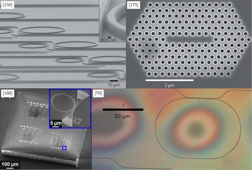
J. Phys. Photonics 2 (2020) 042001 https://doi.org/10.1088/2515-7647/aba171
Journal of Physics: Photonics
Integrated photonic devices in single crystal diamond
Sichen Mi, Marcell Kiss, Teodoro Graziosi and Niels Quack
École Polytechnique Fédérale de Lausanne, 1015, Lausanne, Switzerland
OPEN ACCESS E-mail: niels.quack@epfl.ch
RECEIVED
Keywords: single crystal diamond, photonic integrated circuit, color center, quantum photonics, diamond photonics, microfabrication
15 December 2019
REVISED
7 March 2020
Abstract
ACCEPTED FOR PUBLICATION
30 June 2020
The field of diamond photonics is reviewed, with a focus on recent experimental demonstrations
PUBLISHED
of photonic integrated devices in a single crystal diamond. This field leverages the outstanding
3 August 2020 material properties of diamond with the aim to establish large-scale integrated photonics for
applications in sensing, information and communication technologies, and optomechanics.
Original Content from
this work may be used Accordingly, this review introduces recent progress in scalable micro- and nano-fabrication
under the terms of the techniques for single crystal diamond photonic integrated devices, and provides quantitative
Creative Commons
Attribution 4.0 licence. comparative evaluation of the performance of the state of the art devices. The review concludes
Any further distribution
of this work must with an outlook of the potential of photonic integrated circuits in single crystal diamond.
maintain attribution to
the author(s) and the title
of the work, journal
citation and DOI.
1. Introduction
Diamond has long been recognized as an exceptional material featuring outstanding mechanical, thermal
and optical properties [1]. Benefiting from this unique combination of material properties, many
diamond-based applications have been demonstrated, such as spectroscopy in harsh environments[2, 3],
Raman lasers from DUV to mid-IR [4–7], and beam combining amplifiers working in the kilowatts regime
[8]. Beside the advantageous properties listed in table 1, an important stimulus that boosted researchers’
interest in diamond photonics is the discovery of stable, room-temperature single photon emission from
color centers hosted in single crystal diamond [9], as single photon sources (SPSs) are the enabling building
block for a variety of quantum technologies in imaging, computing, and communication.
Color centers are point defects in solid that can absorb photons in the visible range, which in sufficient
concentration give rise to colorization of diamond crystals, and are therefore termed as such. Although
hundreds of different kinds of such defects have been documented for natural and synthetic diamond [10,
11], only a few have been extensively studied. Among them, the most well-known is nitrogen-vacancy (NV)
center, whose structure is shown in figure 1. Understanding and harnessing their properties has given rise to
numerous novel applications of diamond photonics. For example, NV centers have been used for magnetic
and current sensing with nanometre spatial resolution [12, 13], for keeping quantum information at
room-temperature with duration exceeding 1 second [14], and for establishing quantum entanglement
between distant electron spins [15]. Following these successes, there has been an increasingly active
community working on the monolithic integration of single-photon sources, low-loss waveguides,
modulators and photodetectors towards the establishment of diamond integrated photonics platforms,
aiming at shrinking the footprint and at the same time scaling up the system complexity. These efforts can be
expected to lead to manufacturable and scalable quantum photonic circuits in diamond, in analogy to the
tremendous developments that have been witnessed over the past decades for modern computing and
communication infrastructures enabled by silicon photonic integrated circuits (PIC).
In this review we focus on experimentally demonstrated diamond PIC components with an operating
wavelength in the range from visible to telecommunication wavelengths in the near infrared, motivated by
the typical emission wavelength of color centers in the visible range, and as the interface to existing
telecommunication infrastructures is paramount for wide-spread adoption of diamond photonics [23, 24].
We here focus on the review of photonic devices fabricated in single crystal diamond (SCD). Although
integrated photonic devices have been demonstrated in polycrystalline diamond as well, the performance in
polycrystalline diamond will be inferior to single crystal diamond devices. For example, the propagation loss
will be higher for polycrystalline diamond waveguides due to scattering at grain boundaries and increased
surface roughness, and the grain boundaries in poly-diamond will lead to higher background noise in single
© 2020 The Author(s). Published by IOP Publishing Ltd
J. Phys. Photonics 2 (2020) 042001                                                                                            S Mi et al

Table 1. Material Properties of single crystal diamond and nanocrystalline diamond compared to single crystal silicon. For each value
the reference is reported in the square parenthesis.

Property                                       Single Crystal Diamond         Nanocrystalline Diamond          Single Crystal Silicon

Young’s Modulus (GPa)                             1080–1155 [16]                 500–1120 [17]                    165 [18]
Hardness (GPa)                                    50–110 [16]                    35 - 98 [17]                     13 [19]
Density (kg m−3 )                                 3520 [20]                      3300–3510 [17]                   2330 [20]
Thermal Conductivity (Wm−1 K−1 )                  2200 [20]                      12–1370 [17]                     140 [20]
Thermal Expansion Coefficient (K−1 )              0.8–0.9× 10⁻⁶ [16]                                              2.6× 10⁻⁶ [21]
Sound Velocity (m s−1 )                           18 000–19 000 [16]             15 700–17 980 [17]               8300 [20]
Raman Shift (cm−1 )                               1332 [16]                                                       520 [22]
Bandgap (eV)                                      5.47 [20]                                                       1.12 [20]
Transparency Range (µ m)                          0.22 - 20 [20]                                                  1.1 - 6.5 [20]
Refractive Index                                  2.4 [20]                                                        3.5 [20]

   Figure 1. (a) A NV center consists of one vacancy and one substitutional nitrogen atom in diamond carbon lattice [26]; (b)
   scanning probe made of diamond for nanoscale magnetic sensing, where a NV center resides in the dotted-line marked tip and
   the false-coloured region is SCD [27]; (c) apparatus schematic for using NV center incorporated diamond probe with AFM [27];
   (d) scheme for entanglement generation from distant NV centers [28]; (e) Fiber-interfaced integrated quantum register using SiV
   center and neighbouring 13 C atom [29].

photon sources. Hybrid structures such as GaP-on-diamond [25] or similar platforms, where light is not
guided in diamond but in a material structured on top of a planar diamond surface, will not be covered in
great detail, since this configuration will yield limited coupling of the color centers emission into cavity
modes, which are an essential requirement for emission enhancement.
    In section 2 we address the current status of growth and preparation methods of SCD substrates, and we
summarize the micro- and nanofabrication methods for SCD-based PIC component manufacturing. Section
3 provides a gallery of recently demonstrated state-of-the-art integrated photonic devices in single crystal
diamond. We provide quantitative assessment of the reported device performance and discuss challenges in
section 4, with an outlook for the potential future of diamond photonic integrated circuits in section 5.

2. Diamond micro- and nano-structuring

Mechanical hardness, chemical inertness and high refractive index are among the material properties that
make diamond superior to other materials. Meanwhile, precisely these properties make the micro- and
nano-structuring in return highly challenging. In this section we review the technologies that have been
developed for fabricating integrated diamond photonic devices, bearing the goal of application in scalable
(quantum) integrated photonics. In section 2.1 and 2.1 we give a brief overview of SCD growth methods and
surface preparation, as they are the starting point of large-scale PIC manufacturing, and are important for
understanding restrictions or limitations in device fabrication. Next we discuss about thin membrane
fabrication in section 2.3 and device structuring in section 2.4. As color centers in diamond promise a bright
future for quantum technologies, we also cover a selected set of general methods in section 2.5 for
engineering such defects in a controllable fashion.

                                                       2
J. Phys. Photonics 2 (2020) 042001                                                                                                 S Mi et al

   Figure 2. (a) Unpolished heteroepitaxial grown freestanding SCD wafer with 92 mm diameter. The growth was carried out on
   Ir/YSZ/Si(001) substrate in a 915 MHz microwave plasma CVD setup [48]. (b) Mechanically polished SCD substrate with
   side-length on the order of several millimeters. (c) AFM (atomic force microscopy) characterization of a commercially available
   SCD substrate. Mechanical polishing induced surface damage is found abundant, along with polishing lines [49] (d) After dry
   etching, polishing induced damages on diamond surface is exacerbated as observed by AFM [50, 51]. (e) Slab, rib and strip
   waveguides (from top to bottom) are the most commonly employed geometries for confining light on chip. Design dimensions
   for waveguides in diamond surrounded by air or silica include the total thickness t, the width of the strip w, and the partial etch
   depth p and width of the rib waveguide r. These are in general application dependent, and are both a function of wavelength and
   refractive index. As a guideline, for UV, visible and near-infrared, single- or few-mode operation will typically require t, w, p and r
   between 200 nm and 500 nm with excellent dimensional control at the single digit nanometer scale and surface roughness below 1
   nm.

2.1. Substrate growth
Most commercial SCD substrates are grown either by high pressure high temperature (HPHT) method [30]
or by homoepitaxial chemical vapor deposition (CVD) [31]. SCD grown by HPHT can achieve extremely
low dislocation density [32], but it is difficult to manage impurity incorporation, and such impurities are
usually distributed inhomogeneously, leading to unpredictable local variation of material properties [33]. In
addition, the size of HPHT diamond is inherently limited by the growth apparatus [34, 35], therefore
unsuitable for wafer production and hence large-scale integration. On the other hand, homoepitaxial CVD
growth offers much better control over impurity incorporation by tuning the growth chemistry, being able to
provide high quality SCD substrates suitable for diamond optoelectronic applications. 2-inch substrates can
be obtained by CVD homoepitaxy on tiled arrays of seed substrates [35, 36], the resulting mosaic wafers
having bonding boundaries originating from the gaps between tiles. It has been argued that such boundaries
are of minor concern if they correspond to dicing lines [37] after device fabrication, while they nevertheless
impose additional restrictions onto subsequent processing [35] due to, for example, compromised fracture
toughness. The size limitation for CVD homoepitaxy is set by the diameter of plasma discharge, which can be
extended by appropriately developed designs utilising microwave excitation of lower frequency [36, 38].
    Very recently, diamond growth by heteroepitaxial CVD has also shown promising progress, with
dislocation density reaching the regime of homoepitaxy SCD [39]. The dislocations can reveal etch-pits [40]
during device fabrication, and even when invisible they still cause local strain and affects the optical
properties of diamond such as birefringence [41, 42]. Stronger defect-related electroluminescence was also
shown for p-i-n diode fabricated from heteroepitaxial grown diamond compare to that from HPHT
diamond [43]. The pronounced advantage of heteroepitaxy is the potential to manufacture wafer-sized SCD
substrates directly on a different material, greatly easing wafer separation and subsequent processes. A record
sized 92 mm diameter SCD wafer has been demonstrated based on heteroepitaxial growth on silicon handle
wafers with iridium-based buffer layers, as shown in figure 2. The suitability of such wafers for quantum
sensing has been assessed recently [44].
    CVD growth of diamond is also compatible with patterned or structured substrates, yielding the
potential to directly grow diamond photonic micro-/nano-structures [45–47]. However such bottom-up
approaches are likely to introduce impurities in an uncontrolled or unfavorable way. In the following we will
thus focus on top-down approaches, while re-growth of a thin layer by CVD can in certain cases provide
distinct advantages, with examples given in section 2.3.

                                                         3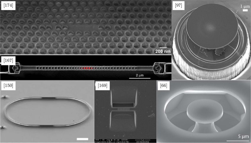
J. Phys. Photonics 2 (2020) 042001                                                                        S Mi et al

2.2. Surface preparation
Being a high refractive index material, the dimensional requirements on diamond waveguiding structures are
very stringent. In particular, the waveguiding layer has to be thin enough to guarantee single- or few-mode
operation for various PIC functionalities. Tight confinement of light and sharp contrast in refractive indices
impose further strict requirements on the surface quality of photonic structures. For low-loss waveguides
and high-Q optical resonators in the visible and telecommunication wavelength, surface roughness below 1
nm r.m.s. is usually required [52, 53].
     As-grown SCD material typically presents a rough surface, which necessitates planarization and
smoothening processes prior to further processing. Crystal growth methods that realize near-perfect
as-grown diamond surfaces have been investigated, yet either with low to moderate yield and limited surface
area [54], or at the cost of very slow growth rates [55]. As a result, polishing of rough as-grown or laser-cut
surfaces still prevails for diamond surface preparation. Usually these treatments are carried out by
mechanical means, and consequently result in undesired process-induced damage to the pristine material
[50, 51, 53]. For example, surface defects that typically exist in commercially available substrates are clearly
seen in figure 2, and severely limit fabrication yield. Although careful fine-polishing can limit the density and
magnitude of such defects [50], the extreme hardness and brittleness of SCD also make it very difficult to
avoid subsurface damages [41] formed during mechanical polishing, whose presence causes detrimental
effects for applications in electronics, quantum information processing and precision sensing. Unlike surface
damages that can be readily identified by optical microscopy, characterizing subsurface damage typically
involves more advanced characterization techniques [56]. To date, the precise extent of subsurface damage
remains elusive, and is estimated from sub-micron [57] to 10 µm deep sample volumes [58]. To avoid
potential device failure caused by polishing induced subsurface crystal damage, a few microns of diamond
material are usually removed by plasma etching before further structuring [50, 52, 53].
     Apart from causing damage, traditional mechanical polishing techniques are not suitable for large-area
processing of SCD wafers due to the strong anisotropy and brittleness of diamond, especially when the wafer
is thin, risking fracture. To mitigate these challenges, a variety of novel polishing techniques have been
developed [41, 49, 59]. For polishing the aforementioned mosaic wafers [37], efficient processes with
little-to-no mechanical load are particularly important [35, 49]. Since homoepitaxial growth remains
currently the most reliable way for high quality SCD growth, we also note that fine polishing of seed
diamond plates gives much improved crystalline quality of CVD growth layer [41], highlighting the
importance of polishing techniques for the manufacturing of high quality single crystal diamond substrates.
For a more comprehensive review on diamond polishing and surface preparation, interested readers are
referred to reference [57, 60].

2.3. Membrane fabrication
Photonic integrated devices require confinement of the optical mode both in vertical as well as in lateral
directions, which is achieved by providing refractive index contrast. Typical wave-guiding structures require
a thin film or structured strip of material surrounded by another material of lower refractive index. Most
commonly exploited waveguide geometries include slab, rib and strip waveguides. In order to achieve single-
or few-mode operation for a given wavelength λ, the dimensions have the be chosen accordingly. For
diamond surrounded by air or silica, the critical dimensions are typically smaller than λ, i.e. for UV, visible
and near-infrared, typically between 200 nm and 500 nm with excellent dimensional control at the single
digit nanometer scale. The schematics of these structures are shown in figure 2.
     A suitable approach to fabricate waveguiding structures is to structure a thin film of single crystalline
waveguiding material on a low refractive material. Technological developments have perfected this approach
for Silicon Photonics by manufacturing specialized silicon-on-insulator (SOI) wafers using a crystalline layer
transfer technique (SmartCut). A similar approach has more recently been successfully demonstrated for
wafer-scale lithium-niobate-on-insulator substrates, and the suitability of this approach for
diamond-on-insulator (DOI) substrates has been postulated. It is important to note, that
silicon-on-diamond structures have also been studied, where diamond replaces the insulator layer, yet these
do not constitute diamond-on-insulator substrates per se. DOI substrates consist of a (single crystal)
diamond layer, on top of a low refractive index dielectric layer, for example silica, which is typically on top of
a thick silicon handle layer. In addition to requirements on the thickness to a few hundreds of nanometers
dictated by the aim for single-mode operation, the diamond layer has to be of high quality, in particular with
low surface (and for structured waveguides: sidewall) roughness to minimize propagation losses.
     The quest for diamond photonics relies thus heavily on the establishment of a high quality (single crystal)
diamond-on-insulator technology. Yet although tremendous advances have been achieved in the past decade,

                                              4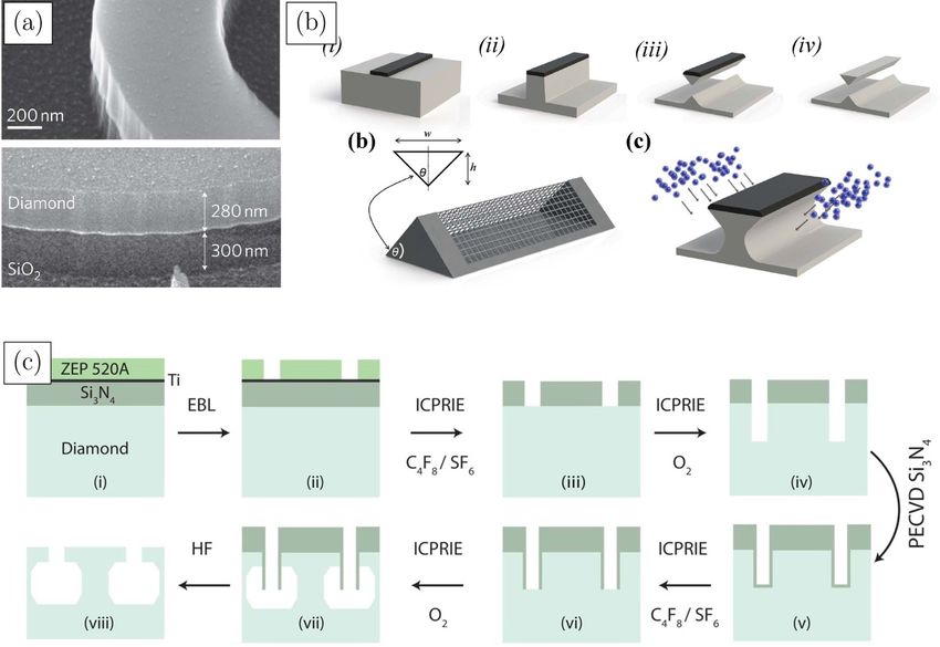
J. Phys. Photonics 2 (2020) 042001                                                                                          S Mi et al

   Figure 3. Typical fabrication techniques for integrated diamond photonics. (a) Typical diamond-on-insulator structures. A thin
   diamond membrane is formed on or attached to an insulating layer, typically SiO2 , which is then patterned into devices using
   lithography and dry etching [64]. (b) ''Angled etching'' via a Faraday cage produces undercut if combined an initial vertical
   etching, enabling free standing structures with a triangular cross-section [65]. (c) Quasi-isotropic etching uses an unbiased
   oxygen plasma for crystal plane selective etching, enabling undercuts similarly to the SCREAM process in silicon [66].

the demonstration of large-scale diamond-on-insulator substrates remains today elusive. In the following,
the recent developments towards the goal of large-scale diamond-on-insulator substrates are reviewed.
     Conceptually, the most straightforward method of fabricating a diamond thin film on an insulating layer
is the direct growth of diamond. The challenge for this approach lies however in the production of a high
quality thin film, due to the aggressive growth conditions for diamond and the difficulty of heteroepitaxy.
While there has been significant success in single crystal diamond heteroepitaxy [44, 48], this approach
requires a complex support stack to accommodate for lattice mismatch between the substrate and diamond,
which has to date proven prohibitive for direct growth of diamond on insulator. Growth of polycrystalline
diamond on insulator however has been demonstrated, yet yielding low quality thin films [61–63].
     Thin diamond films can also be fabricated by thinning bulk crystals. Here, the challenge is in
manipulating the thinned membrane and achieving uniformity and smoothness along the dimensions of the
membrane. Recently, membranes as thin as 5µ m became available for commercial purchase [67, 68], which
makes them an attractive starting point for fabrication of diamond photonic integrated devices: subsequent
thinning by reactive ion etching can produce films thin enough to support single mode propagation [64, 69],
which can also be combined with silicon devices via layer transfer [70].
     A promising method for achieving thin diamond single crystal diamond films employs a fabrication
scheme similar to the SmartCut® process for SOI wafers. Following the first report on achieving diamond
membrane lift-off via implantation by Parikh et al [71], there have been many publications investigating ion
implantation induced graphitisation and using this phenomenon to fabricate single crystal diamond
membranes and membrane-based structures. The diamond substrate is implanted with high energy
(hundred keV - few MeV) light ions (He+ ,C+ ,O+ ) to produce a buried layer rich in vacancies. High
                                      ◦
temperature annealing (500 to 1100 C) converts the damaged layer into etchable amorphous carbon, while
simultaneously recovering some of the ion damage in the top diamond layer. The top layer can also be
overgrown at this stage with pristine diamond, potentially incorporating dopants. The diamond membrane
can then be released by etching the amorphous carbon layer, via chemical [72] or electrochemical [73]
methods. The resulting membrane can be thinned to remove the most damaged regions [74], or attached to
a frame to facilitate handling [75].

                                                      5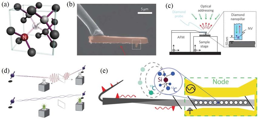
J. Phys. Photonics 2 (2020) 042001                                                                       S Mi et al

2.4. Diamond photonic device structuring
The photonic devices are structured by the etching of the diamond bulk or thin-film, based on a mask
realized using lithographic techniques, typically electron beam lithography.
    Due to the outstanding chemical stability of diamond and the high binding energy of C-C bonds, wet
etchants typically cannot supply sufficient energy to break bonds and form etch byproducts. One known
method of wet etching is to utilise molten salts, like KNO3 [76] or K2CO3 [77] at very high temperatures
     ◦
(600 C+ ). In this case, oxygen from KNO3 reacts with the carbon in diamond, resulting in chemical etching
(with crystallographic anisotropy). However this method is highly aggressive, incompatible with most
cleanroom processes and difficult to carry out in a microfabrication environment.
    Metal-catalytic etching was observed for metals with high carbon solubility (e.g. Fe, Ni). When such
metals are deposited onto the diamond, carbon can be dissolved into the metal, transported to the metal-air
interface and desorbed as gas. This technique is exploited as a form of polishing called hot lapping. Diamond
patterning via this technique was reported by Ralchenko et al [78]. Iron is shown as producing the highest
etch rate, 8 µm min−1 which is significantly faster than typical plasma etches, but the etch does not produce
a smooth surface. This technique can be used for nanopatterning by the use of nanoparticles [79]. In a more
recent work, Nagai et al also report extremely high etch rate (8.7 µm min−1 ) for Ni catalytic etching [80].
The etch demonstrated for (100) substrates is strongly anisotropic, showing selectivity over crystalline planes.
    Etching of diamond structures is also possible through directional plasma etching. In this case, the
etching has a physical component, which is supplied by ion bombardment and a possible chemical
component, where the ion species react with carbon atoms. The research into the structuring of diamond via
dry etching concentrates on different aspects: etch rate, selectivity, verticality, sidewall and etch floor
smoothness.
    Oxygen chemistry is very effective in removing diamond material [81] and is typically used as a high-etch
rate processing step [82]. It can be effectively combined with argon for an increase in etch rate, at the expense
of mask selectivity [83]. A drawback of oxygen/argon based etches is micromasking, i.e. the erosion, and
subsequent redeposition of the masking material onto the etch surface, where it prevents the proceeding of
the etch. To combat this effect, the chemistry can be altered to include a gas that chemically etches the
masking material [84]. Due to the typical use of oxide-based mask, adding a fluorine-containing gas is an
attractive option, especially since this gas is commonly available due to it is use in Si micromachining [85].
Modifying the chemistry can also be used to alter the shape of the etched features [86].
    Chlorine chemistry diamond etching has been reported to improve smoothness of the surface during
etching, and has been used for polishing [82, 87]. Chlorine-based chemistries also exhibit a lower selectivity
against typical particle contaminants (oxides) and against photoresist, which enables proportional etching,
where low selectivity is desired [88].
    A unique modification of the dry etching was demonstrated by Burek et al where an angled Faraday cage
was used to deflect the ion trajectories [65]. Ion beam milling is also possible for a purely physical etch [89],
while ion beam polishing was shown by Mi et al. [49]. The drawback of ion beam patterning is the low
selectivity of the process due to the small etch rate for diamond (an advantage for polishing applications
however) and the resputtering of the masking material and diamond on the sidewalls (also called fencing).
An interesting improvement can be the use of reactive ion beam etching with oxygen, demonstrated by
Atikian et al. for the ion milling of free-standing structures [90].
    Some etch methods of crystalline materials are sensitive to the crystalline face being etched and exhibit a
difference in etch rate for these faces. Such methods are extensively used in machining 3D microstructures
from silicon [91] and are termed ''crystallographic'', to distinguish from directional anisotropy arising
from ion bombardment typically encountered in dry etching. Crystallographic plasma etching was reported
that was selective for dislocations [92, 93], yet the analogue of the Si crystallographic etching was first
reported by Khanaliloo et al. [66]. The crystallographic etching is carried out in a standard deep reactive
(ICP) ion etcher. The process is performed at high ICP powers and zero platen/bias power. This results in an
almost thermal plasma (due to the missing ion acceleration) that is very dense (due to the high ICP power).
In this sense, the etching performed is almost completely chemical in nature, thereby showing selectivity over
the crystal orientation of the etched material. Several reports also exploit an elevated temperature to increase
the etch rate [66, 94]. Process pressure is also higher than typical dry etches for the same reason (15 m Torr to
22 m Torr), however etch rates remain typically limited (< 10 mm min−1 ) and are non-linear for undercuts
[66]. Further characterisation of this etch method was carried out by Xie et al. [95].
    Focused ion beam (FIB) microfabrication is an attractive alternative to plasma etching for forming 3D
structures, owing to the high degree of freedom it offers [96, 97]. The samples are mounted on a multi-axis
stage, allowing machining at different angles, the ion beam can be precisely focused, allowing for high
resolution. The sample can be imaged by the focused ion beam, but typical FIB systems include a scanning
electron microscope column as well, which allows for even higher resolution and more convenient imaging.

                                             6
J. Phys. Photonics 2 (2020) 042001                                                                      S Mi et al

   Bulk properties can also be changed locally to create refractive index contrast. A promising technique is
femtosecond laser bulk modification of diamond, which can be used to write waveguiding structures into
bulk diamond [98]. Waveguides can also be formed by implantation induced refractive index change [99].

2.5. Color center engineering
For integrated diamond photonic device fabrication, formation of color centers in SCD with quantitative
and positional control is of great importance. Depending on the electronic structures of different color
centers, additional specific treatments might be required to further improve their properties. In this section
we briefly address commonly explored approaches for engineering of color centers in diamond, with a focus
on applicable methods for integrated diamond photonics. Dedicated review articles have further previously
been published on NV centers [100, 101] and group-IV centers [102].

2.5.1. Ion implantation
Ion implantation is a widely used technique for introducing foreign atoms into host materials [103]. For
available ion sources, either broad-beam or focused ions can be accelerated towards the diamond substrate,
and depending on the kinetic energy, the accelerated ions gradually slow down and stop in the diamond at a
depth range that can be estimated by Monte Carlo simulation [104]. Interaction between ions and target
material can distort the pristine sp3 carbon crystal lattice structure, creating vacancies and carbon
self-interstitials. When stopped, the ions either replace native carbon in the lattice (substitutional
impurities), or reside in interstitial position. At this stage the crystalline structure can be heavily damaged,
and GR1 signal can be generally observed, indicating the creation of vacancies. Post-implantation annealing
[105] at high temperature restores (to a certain extent) the lattice structure and mobilizes vacancies, which
can then be trapped by impurities, forming impurity-vacancy complexes, such as NV centers. For practical
applications, nevertheless, formation of certain defects may not be sufficient; properties such as long
coherence time and small spectral diffusion are often important. This additional requirements make ion
implantation less suitable for certain applications. For example, a recent study [106] implanting 15 N into
diamond with native nitrogen incorporation demonstrated that implantation-introduced nitrogen atoms
tend to form NV− centers with drastically compromised optical coherence compared to their native
counterpart, possibly owing to local damage caused by implantation. HPHT annealing has been shown to
narrow the emission linewidth of NV− ensembles [107] fabricated by implantation, but further study is
required to better understand the underlying mechanisms. SiV− centers on the other hand, show decent
optical coherence when fabricated by implantation and post-annealing, in both bulk and nanostructured
diamond [108, 109]. In the absence of post-annealing, creation of NV− centers has been observed after swift
heavy ion implantation [110]. Electronic excitations and thermal spikes were suggested to be possible
mechanisms for color center formation, yet further investigations are required to understand this process.
    The prominent advantage of implantation for color center fabrication is the positional control. The
incident position of ions can be confined to nanometer precision by using focused ion beam [111], masks
with nano-holes [112], or pierced AFM tips [113]. The depth distribution of the stopped ions is determined
by their initial kinetic energy: increased implantation energies result thus in less accurate positioning. The
lateral straggling follows the same trend. For example, nitrogen implantation with 2.5 keV acceleration can
reach 10 nm accuracy, while for 10 keV it is about 30 nm [114]. Consequently, precise positioning the color
center deep into the substrate is not possible with direct ion implantation. This can be nevertheless be
circumvented by shallow implantation followed by overgrowth [114–116]. Another approach for
three-dimensional positioning is laser writing which will be addressed in section 2.5.3. Combining
delta-doping and electron irradiation can also be used to realize 3D positioning, and will be discussed in
2.5.4. A caveat regarding ion implantation in single crystal materials are ion channelling effects, which can
occur upon implantation at specific angles with respect to the crystal orientation, and has been shown to
result in greatly extended ion implantation depths compared to Monte Carlo simulations [117]. Therefore,
best practices for ion implantation is to avoid implantation at certain angles, depending on the crystalline
plane orientation.
    Quantitative control of defect density can also be achieved by adequately increasing or decreasing the
implantation dose, however, typically careful calibration is required to precisely control the resulting defect
density, as the conversion yield varies with experimental conditions [111, 118]. Electron and laser irradiation
have further been demonstrated effective for improving the conversion yield, as will be discussed in the next
sections.

2.5.2. Electron irradiation
As ion implantation causes severe lattice damage, which may degrade the performance of color centers,
electron irradiation has been employed as an alternative to create vacancies [51, 119]. The threshold for

                                             7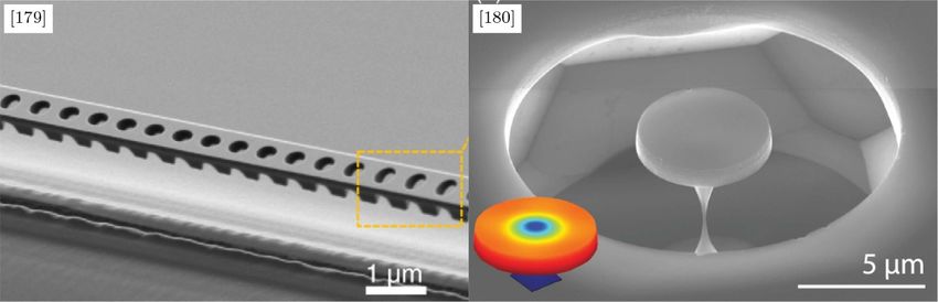
J. Phys. Photonics 2 (2020) 042001                                                                      S Mi et al

accelerated electrons displacing carbon atom in the lattice is about 150–170 keV [111, 120]. Formation of
impurity-involved defects in this way relies on pre-existing foreign elements. This method for example has
been used to increase the yield of SiV− [111] and NV− [119] formation after ion implantation, indicating
that the conversion yield from implanted impurity to impurity-vacancy complex is limited by the availability
of vacancies. As for ion implantation, lateral positioning can also be achieved with electron irradiation [121].
Meanwhile, MeV electrons can travel through mm-thick diamond and are therefore suitable for modifying
the properties of bulk diamond. It is interesting to note that electron irradiation with energy below the
threshold for vacancy creation [120] has been shown to also promote the formation of NV− centers in a
nitrogen-implanted sample, possibly due to electronic excitation.

2.5.3. Laser irradiation
Direct lasing writing for fabricating color centers has been intensively studied in recent years, and the fast
progress has shown great promise in terms of flexibility, quality and conversion yield [122–126].
     In 2013, Liu et al [123] demonstrated that femtosecond laser pulses can be used to ionize molecules in
air, with the resulting electrons accelerated by subsequent pulses towards the diamond surface, creating
vacancies. Following annealing, photoluminescence from NV− centers can be observed. The starting
material was type Ib diamond with abundant nitrogen impurities, and it is not clear if there were nitrogen
ions accelerated and implanted into the diamond. In 2019, the same group reported formation of SiV−
centers using a similar method [122], but with silicon nanoballs coated on high-purity diamond surface. The
results unambiguously shows that Si ions were accelerated by the laser pulse and implanted into diamond.
     Another approach is to focus a laser pulse directly into bulk diamond with native impurities.
Photoluminescence from GR1 centers confirmed photo-generated vacancies. Following annealing, NV−
centers with good optical coherence were observed [124]. The same group later also found out that thermal
annealing can be replaced by laser irradiation itself [125]. A first pulse was applied to generate vacancies in
the crystal, which was followed by a pulse train with lower energy, to locally anneal diamond at the focus
spot. In this way one can observe photoluminescence signal from the same spot in real time, and stop the
laser annealing with the onset of NV− formation. This method provides excellent control of the NV−
formation process, and the authors report an impressive yield of 96% for creating single NV− centers. In
addition, it has also been demonstrated that this method is well suited to fabricate 3D arrays of color centers
[126], showing much greater flexibility over ion implantation.

2.5.4. CVD growth
Color centers can be incorporated directly into diamond during CVD growth. For example with the presence
of nickle in the CVD chamber, NE8 center can be observed in as-grown diamond [127, 128], while ion
implantation so far has been demonstrated unsuccessful for its creation [129, 130]. Furthermore, CVD
growth is of particular interest for the preferential orientation of color centers [131], which is important for
various applications such as metrology [132]. Very recently, record-long inhomogeneous spin-dephasing
time (T∗2 ≈ 1.5 ms) and Hahn-echo spin-coherence time (T2 ≈ 2.4 ms) were found for NV− center in a
phosphorus-doped CVD diamond [133], leading to better sensitivity for magnetic sensing. Isotopic
engineering of CVD diamond by tuning growth condition can also improve the coherence properties of color
centers [134].
    In general, the impurities incorporated during CVD growth present relatively inhomogeneous
distribution. However, in the particular approach of ''delta doping'' foreign atoms can be introduced into
the diamond at a specified depth [135], even with perfect alignment [131]. In combination with electron
irradiation, positional control in 3D has also been demonstrated [121].

2.5.5. HPHT growth
Similar to CVD doping, impurities can also be incorporated into diamond during HPHT growth. They
usually originate from the environment (e.g. nitrogen) or the solvent-catalyst (e.g. nickle) used to dissolve
carbon, and it is not trivial to make this process under precisely controlled conditions. Like CVD growth,
preferentially aligned NV centers have been observed in HPHT grown diamond [136]. Since HPHT growth
is more difficult to control than CVD, quantitative engineering of color centers using this method seems
unlikely at this moment.

2.5.6. Charge state control
The control of the charge state is of importance for several applications. For example, NV centers exhibit
ODMR only when negatively charged [137] therefore NV− centers have been extensively studied for
magnetic sensing, and the spin coherence time of neutrally charged SiV centers largely exceeds the one of

                                             8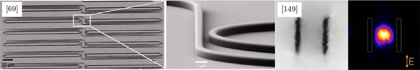
J. Phys. Photonics 2 (2020) 042001                                                                                              S Mi et al

          Figure 4. Waveguides in single crystal diamond fabricated via membrane thinning [69] or direct laser writing [149].

negatively charged ones [138] since total spin of 1/2 makes SiV− prone to phonon-mediated, dynamic
Jahn-Teller–like orbital relaxation [139].
    The charge state of color centers can be passively engineered by doping, which modifies the Fermi level of
diamond, leading to preference in forming a certain charge state. In 2016, Doi et al showed that CVD-grown
diamond, n-doped with phosphorus, has steady state population of NV− above 99% under 593 nm
illumination, leading to enhanced luminescence and magnetic sensing [140]. Implantation of Si ions into
boron-doped CVD diamond showed > 80% conversion yield to SiV0 as the Fermi level was pinned to make
neutral charge state have the lowest formation energy [138]. Doping by implantation of phosphorous and
boron followed by high temperature annealing has also been demonstrated effective to change the charge
state of NV centers [141]. Apart from doping, annealing in dark has been reported to convert SiV from
neutral to negative state [142]. HPHT annealing at 8 GPa and 2000 degrees increases the NV− /NV0 ratio by a
factor of 5, but this is accompanied by an overall decrease in the NV count [107]. Better understanding of
this process requires more knowledge on the interplay between color centers and donors/acceptors during
annealing. For near-surface color centers, the chemical termination of diamond surface also plays a role in
determining the charge state [141, 143, 144]. Active control of the charge state has been demonstrated by
optical [145] or electrical means [146]. Approaches to achieve charge state control at device-level are
discussed in section 3.7.

3. Review of diamond photonic integrated devices

In this section we review integrated photonic devices that have been fabricated in diamond.

3.1. Waveguiding Devices
Guiding light between photonic devices in a well controlled manner with limited losses requires the
fabrication of waveguiding structures. In this section, diamond waveguide approaches are shown, along with
other passive optical structures, such as splitters and couplers. Although theoretical investigations of such
high-index contrast structures in diamond have been performed (e.g. [147, 148]), only fabricated devices
will be discussed.
    Angled etching is a versatile technique capable of creating very high-quality waveguides with a triangular
cross-section [52], with an estimated propagation loss of 1.5 dB cm−1. With the use of a broad ion beam to
instead of a Faraday-cage, difficulties arising from misalignment of the sample with respect to the Faraday
cage can be mitigated, while keeping the advantageous properties [90, 150].
    A promising method for fabricating waveguiding structures is ultrafast pulsed laser-based structuring.
Here the most common structure is referred to as Type II structure comprising two parallel written lines
providing confinement to the optical mode. Such waveguides were initially high loss with 7.9 dB cm−1 [149]
and 16 dB cm−1 [151], but significant improvements have been demonstrated 4.2 dB cm−1 [152]. Other
passive optical structures, such as Y-splitters (-7 dB) and bends (3 dB bend loss for radius of 25 mm) have
been demonstrated [149]. These techniques are also applicable for MIR applications [153], with propagation
losses of 6 dB cm−1 at 2.4 µ m and 8.6 µm. The confinement can also be achieved by ion implantation
induced refractive index change [99], however the losses are high 22 dB cm−1 due to absorption.
    Membrane thinning and subsequent patterning lends well to the fabrication of waveguides. Such
diamond-on-insulator waveguides have been demonstrated with very high quality by multiple groups [69,
154, 155]. Excellent propagation losses are reported (1.7 dB cm−1 [69], 0.34 dB cm−1 [155]). The resulting
waveguides can be overgrown [156, 157], with propagation losses of 16.5 dB cm−1, improved in the
subsequent publication to 12.3 dB cm−1, by compensating for the membrane wedge and smoother e-beam
patterning. Another possibility is the transfer of the membrane onto a SOI substrate via drop-casting,
resulting in hybrid diamond—Si or diamond—HSQ – Si waveguides [70], with excellent reported
propagation losses of 0.34 dB cm−1.

                                                      9
J. Phys. Photonics 2 (2020) 042001 S Mi et al
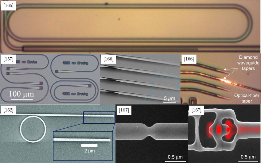
Figure 5. Racetrack cavity fabricated on a diamond-on-insulator (DOI) substrate, coupled to a waveguide which is extended by
SU-8 resist to the edge of carrier substrate [164]. Grating couplers on DOI substrate operating at a central wavelength of 1550 nm
[156]. SEM and optical images of suspended diamond waveguide taper fabricated with angled-etching method [165].
Second-order grating coupler on DOI waveguide [161]. Notch and inversely designed vertical coupler for quasi-isotropic etch
platform [166].
Ion implantation induced graphitisation and release coupled with dry etching can be used to define
free-standing [158] or membrane-based [159] waveguides. In the latter case a propagation loss of 7.2 dB
cm−1 was reported. The authors comment on the possibility of the fabrication of fully etched structures on
the platform by either using anchor structures or the augmentation of the membrane structure with a low
refractive index material on the bottom side, such as PECVD SiO2 .
3.2. Coupling devices
Interfacing light between photonic waveguides and optical fibers (or free-space) has been demonstrated for
diamond-on-insulator based devices by either butt coupling or using grating couplers. In the former case, an
adiabatically tapered diamond waveguide is extended, as shown in figure 5, by SU-8 resist or spin-on glass to
the edge of the sample, and both free-space [5] and lensed fiber coupling [69, 155, 160] have been
demonstrated. Example grating couplers for visible [161, 162] and telecommunication [157, 163]
wavelengths are also presented in figure 5.
The simplest option for coupling light to and from devices fabricated by the angled-etch method may be
a notch in the waveguide, however, only very low efficiency around 1% [53] have been achieved. On the
other hand, efficient (> 90%) interfacing was reported at visible and telecommunication wavelengths by
adiabatic mode transfer from a diamond waveguide taper to an optical fiber taper [165]. Free-space coupling
of femtosecond laser pulses to a diamond waveguide taper was also carried out in a demonstration of
supercontinuum generation [167], however, the tapered section was damaged at high pump power.
Owing to a strong correlation between the initial etch depth and undercut thin-film area for
quasi-isotropically etched devices, fabrication of couplers requires more design optimization. Dory et al [166]
reported recently on the inverse design method for fabricating devices based on this fabrication approach,
and the resulted vertical couplers (figure 5) showed efficiency > 24 times of that of a waveguide notch.
3.3. Optical resonators
Starting from a bulk diamond plate, direct milling with focused ion beam (FIB) is an attractive method to
create 3D structures and several demonstrations of photonic structures realized with FIB milling have been
reported. Bayn et al fabricated triangular nanobeam photonic crystal cavities by milling the bulk diamond
substrates from two directions [168]. Optical characterisation reveals a Q factor of 221 at visible wavelengths.
Similar investigation into FIB milled nanobeams are carried out by Babinec et al [169]. Instead of achieving a
triangular cross section, a rectangular photonic crystal beam was fabricated by using milling directions
10J. Phys. Photonics 2 (2020) 042001 S Mi et al
Figure 6. Microresonators fabricated in bulk single crystal diamond. Photonic crystal beam [168] and microdisk resonators [97]
structured by focused ion beam milling. Racetrack resonator by angled etch [52]. Microdisk [66], 2D photonic crystal [173], and
1D photonic crystal beam fabricated by quasi-isotropic etching [166].
orthogonal to the diamond plate. An alternative fabrication scheme is also proposed, where diamond
lamellas are fabricated into diamond slabs, based on the commonly used transmission electron microscope
lift-off technique [170]. The authors report no Q factor measurements. FIB milling can be used in
combination with reactive ion etching (RIE). One of the two techniques presented by Li et al [171], involves
the structuring of a photonic crystal beam starting from a rectangular cuboid, patterned with the photonic
crystal, which is suspended from the substrate with FIB milling. No optical Q is reported. Microdisk
resonators were fabricated by Graziosi et al using a combination of RIE and FIB milling [97]. A pillar is
defined by an initial directional oxygen reactive ion etch step, which is subsequently undercut using FIB
milling from two directions. The authors report an optical Q of 5700 at telecommunication wavelengths, the
highest reported quality factor by FIB machining.
In a different approach utilising directional milling (angled-etching), several photonic structures have
been demonstrated, including suspended 1D photonic crystal cavities, microdisks, and suspended
waveguides, operating at telecommunication and visible wavelengths [52]. Racetrack resonators feature
loaded Q-factors of QTE ~ 151 000 and QTM ~ 113 000 at 1550 nm wavelength. Further evolution of this
technique employed etching by a broad ion beam and rotation of the tilted sample to achieve similar
undercutting [90]. The method, termed reactive ion beam angled etching, uses an oxygen ion beam to mill
the surface. Atikian et al demonstrate racetrack resonators in polycrystalline diamond (Q ~ 30 000) and
single crystal diamond (Q ~ 286 000). Uniformity is demonstrated by fabricating two racetrack resonators
separated by 19 mm, with comparable quality factors and transmission spectra.
Crystallographic etching, also referred as quasi-isotropic etching has successfully been employed to
fabricate microdisks and photonic crystal beams and membranes. Khanaliloo et al presented single crystal
diamond microdisks of ~ 1µ m thickness and ~ 7µ m diameter, with a faceted supporting pillar of ~ 4.6µ m.
Optical characterisation reveals a loaded Q of ~ 1.091 05 [66]. After extensive process optimisation, Q was
improved even further by a factor ~ 4 [172]. The authors investigated optimising the hard mask etching step,
the anisotropic vertical diamond etch step, surface treatment and cleaning and the modification of the
pedestal shape via an additional masking layer. Mouradian et al applied the crystallographic etching to
fabricate nanobeam cavities in single crystal diamond [94]. Optical measurements reveal an optical Q factor
above 14 700 at visible wavelength. Dory et al [166] have demonstrated nanobeam photonic crystal cavities
using similar techniques, achieving Q factors of 4000 at NV center wavelengths. The fabrication process for
nanobeam cavities was subsequently extended to fabricate 2-dimensional photonic crystals by Wan et al
[173]. With a practically equivalent process flow, ~ 4µ m-wide, ~ 200 nm-thick planar slabs are fabricated,
with optical cavities formed by designed defects in photonic crystal. The measured Q factor is from 2670 to
6080 at 637 nm.
11J. Phys. Photonics 2 (2020) 042001 S Mi et al
Figure 7. Single crystal diamond resonators fabricated in thin film diamond. Microrings coupled to waveguides [155]. 2D
photonic crystal cavity in a heteroepitaxially grown single crystal diamond thin film [174]. Photonic circuits, including microring
resonators [159]. Single crystal diamond thin film on top of silicon waveguides and microring resonators (adapted from [70]).
The examples listed above are demonstration of optical cavities in bulk diamond substrates. To achieve
the vertical confinement, undercut is necessary to create a low index region below the resonators. Substantial
development has been reported for the fabrication of thin diamond membranes and of photonic devices on
diamond thin films. Improvements are demonstrated in growing the diamond layer by utilising an iridium
buffer layer for growth by Riedrich-Möller et al [174]. By engineering the lattice mismatch of the growth
substrate (Ir/YSZ/Si(001)), the grown ~ 12µ m thick layer is single crystal diamond, even if rich in
dislocations. To fabricate free standing membranes, the backside silicon layer is etched in windows using deep
reactive ion etching. The buffer layers are removed via ion beam etching, and the diamond film is thinned,
removing the lowest quality nucleation layers. Subsequently, FIB milling is carried out to pattern the layer
◦
into nanobeams and photonic crystal cavities. A final annealing at 1000 C is carried out for 2 h in vacuum,
◦
followed by an acid treatment (H2 SO4 :H2 O2 , 1:1) and oxidation (420 C, 2 h), to remove FIB damage. Q
factors of 700 and 450 at visible wavelength are reported for the 1D and 2D photonic crystals, respectively.
Faraon et al demonstrated a fabrication of a single crystal diamond-on-insulator type structure by
thinning a 5 µ m membrane [64]. The fabricated microring resonators have a Q factor of 5000, limited by
sidewall roughness. A similar process flow was carried out by Hausmann et al [69]. Large diameter ring
resonators and racetrack resonators have been fabricated, with a measured Q of ~ 250 000. This fabrication
process was adapted for suspended structures later by the same group [175], with a Si substrate. Cavity
modes are measured for the released nanobeams with Q factors up to ~ 6000. Two dimensional photonic
crystal cavities are fabricated based on a similar process flow by Jung et al attaching a thin single crystal
diamond membrane onto a Si substrate [176] and using focused ion beam milling to create the holes for a
photonic crystal structure. The authors report a Q factor of 870 at 637 nm. Similarly thinned membranes are
used by Li et al as well [177]. Photonic crystal cavities were fabricated and characterized, yielding Q values of
4700 at 632.3 nm. This fabrication method was later used by Schröder et al to fabricate 2D photonic crystals
[111] with embedded Si vacancies, by local implantation via Si focused ion beam. Hill et al demonstrated the
integration of a thin diamond membrane with a Si photonic integrated circuit [70]. Hybrid Si—diamond
and Si—HSQ – diamond waveguides and resonators were fabricated via this method. The authors report ~
30 800 for structures with and ~ 10 800 without HSQ.
Single crystal membranes fabricated by ion implantation and sacrifical layer etching (diamond Smart
Cut, see section 2.3), have served as substrates for fabrication of photonic devices [159]. Rib-type photonic
structures were characterised optically and a (loaded) Q-factor of 66 000 was reported for disk resonators.
12J. Phys. Photonics 2 (2020) 042001 S Mi et al
Figure 8. Optomechanical resonators in single crystal diamond. Photonic crystal beam fabricated with the angled etching
technique [178]. Single crystal microdisk fabricated in a bulk substrate using a quasi-isotropic undercut. [179].
3.4. Optomechanical Devices
The ability to suspend diamond optical cavities paves the way for diamond cavity optomechanics. Including
a appropriately designed optomechanical crystal in an angled-etched diamond cantilever, Burek et al [178]
demonstrated phonon lasing and Optomechanically Induced Transparency (OMIT). The devices present
high optical quality factors Qo (1.7∗ 105 and 2.7 105 ) and high Ω/2π (5.5 GHz and 9.5 GHz), making the
optomechanical cavity operate in the resolved sideband regime. Measured mechanical quality factors (at
ambient conditions) are of the order of ~ 5000. Mechanical quality factors (Qm ) of diamond resonators tend
to increase at lower temperatures [180], and follow-up work [181] has verified this reduced dissipation for
diamond optomechanical crystals, recording an increase of 30× at 5 K, measuring Qm up to 238 000. In
combination with the high high oscillating frequency, the devices exhibit Qf -products in the order of 1015
Hz at 5 K (1013 Hz at 300 K).
The group of Paul E. Barclay at the University of Calgary presented several cavity optomechanics
experiments using SCD microdisks. The fabrication strategy is based on a quasi isotropic etch [179], here
yielding microdisks supported by an hourglass shaped pedestal with octagonal cross section. Self-oscillation
amplification was demonstrated in SCD microdisks with sufficiently thin pedestal diameters. Mechanical
resonances corresponding to the fundamental radial breathing mode are reported with Ω/2π ~ 2 GHz and
Qm ~ 9000 (at room temperature and pressure), yielding an Qf -product of 1.91013 Hz. The pedestal
geometry appears to be of particular importance for the RBM dissipation, and only the thinnest pedestals (~
100 nm) present small mechanical dissipation. The microdisks show high optomechanical cooperativity
C = Ng20 /κΓ ∼ eq2.7 under ambient conditions. Further work by the authors investigated fabrication
strategies to improve the sidewall surface roughness, improving the optical quality factor to ~ 300 000, as well
a way of reducing the mechanical dissipation by engineering the pedestal shape [172, 182]. With the
engineered pedestal, demonstration of optomechanical cooling and OMIT was possible [182]. Excellent
OMIT performance was reported even with Qo ∼ 105 . OMIT can be further exploited using a second control
laser signal to achieve all optical switching [183], optical control of pulse time storage storage[184], and
optomechanically mediated wavelength conversion [185, 186].
3.5. Sources
The wide bandgap allows SCD to be used for fabricating light-emitting diodes (LED) with 5.27 eV emission
due to exciton recombination [187]. Its associated transparency also permits Raman lasing operating in the
DUV range [4]. However here we will only discuss diamond-based light sources in the
visible-to-telecommunication range, as diamond PIC component for UV light has not been demonstrated,
partially due to the fact that the high refractive index of diamond implies small feature sizes and low
tolerance on fabrication errors [162, 188].
3.5.1. Single photon sources
Many color centers in diamond have been verified as single photon emitters [191]. However, due to their
interaction with local field, inhomogeneous distribution of transition frequency usually exists among
multiple color centers of the same kind, severely limiting the indistinguishability between photons emitted
from different color centers. Even for the same color center, under illumination, the local field can undergo
fluctuations and the transition frequency can be unstable. NV− and SiV− centers for example, are sensitive to
electric fields and strain fields respectively, and local variations of such fields due to impurities and processing
inevitably impedes the scalability of color center based technologies for QIP. Figure 9 provides an illustrative
13You can also read