Advanced Progress on χ(3) Nonlinearity in Chip-Scale Photonic Platforms - Progress In ...
←
→
Page content transcription
If your browser does not render page correctly, please read the page content below
Progress In Electromagnetics Research, Vol. 170, 17–62, 2021

             Advanced Progress on χ(3) Nonlinearity in Chip-Scale
                            Photonic Platforms

     Zhe Kang1, 2, # , Chao Mei3, # , Luqi Zhang4 , Zhichao Zhang4 , Julian Evans2 ,
 Yujun Cheng4 , Kun Zhu5 , Xianting Zhang5 , Dongmei Huang5 , Yuhua Li6 , Jijun He7 ,
Qiang Wu8 , Binbin Yan4 , Kuiru Wang4 , Xian Zhou3 , Keping Long3 , Feng Li5 , Qian Li9 ,
       Shaokang Wang10 , Jinhui Yuan3, 4, * , P. K. A. Wai5 , and Sailing He1, 2, *

                                                     (Invited Review)

Abstract—χ(3) nonlinearity enables ultrafast femtosecond scale light-to-light coupling and
manipulation of intensity, phase, and frequency. χ(3) nonlinear functionality in micro- and nano-
scale photonic waveguides can potentially replace bulky fiber platforms for many applications. In
this Review, we summarize and comment on the progress on χ(3) nonlinearity in chip-scale photonic
platforms, including several focused hot topics such as broadband and coherent sources in the new bands,
nonlinear pulse shaping, and all-optical signal processing. An outlook of challenges and prospects on
this hot research field is given at the end.

1. INTRODUCTION

The invention of the laser by Maiman in 1960 gave rise to the unprecedented development of the
old subject of optics [1]. As one of the largest branches of optics, nonlinear optics which describes
the interaction between light and matter has attracted countless research efforts. When the medium
whose inner structure is centrosymmetric is exposed to high intensity light, χ(3) nonlinear processes are
the lowest order. This process originates from the electronic polarization caused by the electric-field
component of the light, which can be mathematically given by [2]

                                                           (3) ..
                            P = ε0 χ · E + χ : EE + χ . EEE + . . .
                                     (1)       (2)
                                                                                                      (1)

where ε0 is the dielectric constant in vacuum; E is the complex electric-field amplitude; χ(1) is the tensor
of rank 2 which denotes the linear response to E; χ(2) and χ(3) are tensors of ranks 3 and 4 which define
  Received 21 December 2020, Accepted 13 January 2021, Scheduled 15 January 2021
* Corresponding authors: Jinhui Yuan (yuanjinhui81@bupt.edu.cn), Sailing He (sailing@jorcep.org).
1 Ningbo Research Institute, Zhejiang University, Ningbo 315000, China. 2 Centre for Optical and Electromagnetic Research,

National Engineering Research Center for Optical Instruments, Zhejiang University, Hangzhou 310000, China. 3 Research Center
for Convergence Networks and Ubiquitous Services, University of Science and Technology Beijing, Beijing 100083, China. 4 State
Key Laboratory of Information Photonics and Optical Communications, Beijing University of Posts and Telecommunications, Beijing
100876, China. 5 Photonics Research Centre, Department of Electronic and Information Engineering, The Hong Kong Polytechnic
University, Hung Hom, Hong Kong, China. 6 Department of Physics, City University of Hong Kong, Hong Kong, China. 7 Swiss
Federal Institute of Technology Lausanne (EPFL), 1015 Lausanne, Switzerland. 8 Department of Physics and Electrical Engineering,
Northumbria University, Newcastle upon Tyne, NE1 8ST, United Kingdom. 9 School of Electronic and Computer Engineering,
Peking University, Shenzhen 518055, China. 10 Department of Computer Science and Electrical Engineering, University of Maryland,
Baltimore County, Baltimore, MD 21250, USA.
# These authors contributed equally to this work.
18                                                                                            Kang et al.

the second-order and third-order nonlinear responses, respectively. Compared to the χ(2) nonlinearity,
the excitation of χ(3) nonlinearity generally requires higher intensity. χ(3) nonlinearity has much richer
physical dynamics since it is higher order. In this paper, we will be focused on the χ(3) nonlinearity.
Basic effects that relate to the χ(3) nonlinearity include self-phase modulation (SPM), cross-phase
modulation (XPM), third-order harmonic generation, four-wave mixing (FWM), two-photon absorption
(TPA), stimulated Raman scattering (SRS), stimulated Brillouin scattering (SBS), etc. These effects are
induced by different kinds of light-matter interaction. Figure 1 illustrates the processes of light-matter
interaction. An input field with specific frequency encounters the molecule and then generates a new
field with different frequencies. Taking the nondegenerate FWM as an example, the input frequencies
of ω1 and ω2 can emit two new frequencies of ω3 and ω4 . Nevertheless, the energy and momentum are
conserved in this process, which indicates the FWM is a Hamilton process. In contrast, some other
effects, such as SRS and SBS, only obey momentum conservation law but not energy conservation, and
a part of energy is transferred to the mediated phonons.

                                    (a)                                       (b)

Figure 1. (a) Skeptical demonstration of light-matter interaction, and (b) typical process of FWM.

      SRS was the first studied nonlinear effects in 1962, soon after the invention of laser [3]. After
that, Maker et al. found that the refractive indexes of liquids are changed with the intensity of input
field [4]. The phenomena of SBS [5] and FWM [6] were observed in 1964 and 1966, respectively. At
that time, most nonlinear effects were studied in bulk media, such as liquids, or gases until emergence
of optical fiber in 1966 [7]. Optical fiber, especially the low-loss fiber, is an ideal waveguide in which
light can directionally propagate. As a result, the light-matter interaction is prolonged in long fibers.
Ippen demonstrated the first Raman laser in CS2 -core fiber in early 1970 [8]. A lot of other nonlinear
effects were then discovered in silica fibers such as the SBS [9], FWM [10], SPM [11], and XPM [12].
Understanding these nonlinear effects is very important because it then inspired people to theoretically
[13] and experimentally [14] find temporal optical soliton. Soliton is one of the most important concepts
in nonlinear optics because it stands for an exact balance between SPM and group-velocity dispersion
(GVD). This kind of temporally localized wave packet is similar to the time-domain discrete pulse trains
in a mode-locked laser. Soliton lasers were then widely studied in optical fibers [15] after the advent of
optical solitons. The temporal stability of soliton makes it an ideal tool for communication transmission.
The bandwidth-limited soliton communication system was built up [16] in 1986. A natural question is
what would happen if the exact balance of the soliton is broken? It has been shown that in this case,
other nonlinear phenomena such as dispersive wave [17], soliton fission [18], soliton self-frequency shift
(SSFS) [19] can occur. These nonlinear effects could jointly lead to supercontinuum (SC) generation [20].
The property of SC strongly depends on GVD profiles of the waveguides. Unfortunately, conventional
single-mode fiber (SMF) cannot provide enough flexibility in GVD engineering because the core diameter
of SMF is too large (8 ∼ 10 µm) compared with the wavelength which is pumped at the near-infrared
region (NIR). In such waveguides, the material dispersion which locates at the normal dispersion region
is stronger than geometrical dispersion. To compensate the material dispersion, one needs to reduce the
transverse size of SMF to a level that is comparable to pump wavelength. The successful fabrication of
photonic crystal fiber (PCF) in 1995 has solved this problem [21]. The core diameter of PCF can be
engineered to be only 1 ∼ 2 µm. The transverse microstructure of PCF can be arranged periodically
over much of the cross-section, which provides another possibility to engineer the dispersion by changing
Progress In Electromagnetics Research, Vol. 170, 2021                                                   19

the transverse size or structure. So far, PCF has many variants, such as photonic-bandgap fibers [22],
holey fibers [23], hole-assisted fibers [24], Bragg fibers [25] and anti-resonant fibers [26]. The materials
which are used to make up PCF are also not limited to SiO2 . Gas and liquid with various dispersion
profiles are also employed for specific dispersion design. The abundant selection of constituent materials,
designable transverse size and structure allow PCFs to open many possibilities in the study of nonlinear
optics.
      With the rapid development of micro/nano manufacturing technology, waveguide with
subwavelength transverse size becomes possible. Recently, the study of nonlinear optics in the
micro/nano photonic waveguide (MNPW) has attracted broad interest [27]. Different from cylindrical
waveguides such as SMF or PCF, MNPW not only has a smaller transverse size, but also the ability
to integrate with photonic circuits. More importantly, MNPWs have the advantage of low energy
consumption, flexible dispersion engineering, low cost, wide transparent window, and high nonlinear
refractive index. According to the difference in transverse geometrical structure, MNPWs can be
classified as ridge (inverse ridge), strip, channel and slot waveguides. Longitudinally propagating electric
field in MNPWs can be tightly confined within a rather small area due to the higher refractive index
contrast. For example, the refractive index contrast of SMF is almost 100 times smaller than that of a
silicon-on-insulator (SOI) waveguide. The effective mode area Aeff of MNPW is much smaller, which
results in the enhanced light-matter interaction [28]. The nonlinear coefficient γ = 2πn2 /(λAeff ) is thus
increased, where n2 is the nonlinear refractive index. While the optical field propagating in SMFs is
restricted to the core layer, any desired propagating layer can be achieved for MNPWs by the structure
design. While the linear loss of MNPW is much larger than that of fibers, the waveguide length required
by nonlinear effects is much shorter due to the large γ. Additionally, the linear loss of MNPWs can be
mitigated with proper fabrication [29].
      Figure 2 schematically shows the cross sections of typical MNPW waveguides. In contrast to
the fiber-based waveguides, the flexible dispersion engineering of MNPWs is reflected in the diversity
of transverse geometries with smaller scale down to sub-micrometers and nanometers levels. The
dimensions of a microring is also shown in comparison with a coin. The transverse profile of MNPWs
including ridge, strip, channel, and slot in Figure 2 means that it cannot be fabricated by simply tapering
the preformed bar as for SMFs and PCFs. Techniques of micro/nano fabrication must be employed
including the thermal oxidation, sputtering, chemical vapor deposition, flame hydrolysis deposition,
ion-assisted deposition, spin-coating, sol-gel technique, etc. [30].

              (a)                               (b)

              (c)                               (d)

Figure 2. Schematic diagram (left panel) and SEM (right panel) of (a) a ridge MNPW, (b) a strip
MNPW, (c) a buried MNPW and (d) a slot MNPW. (e) Microring chips together with 1-cent coin for
size comparison, and (f) MNPWs integrated on a 12-inch Si wafer.

     Typical χ(3) nonlinear effects observed in SMFs or PCFs have also been found in MNPWs. For
instance, Si waveguides have demonstrated SPM and XPM effects [31, 32]. However, compared with
cylindrical waveguides, larger linear loss in MNPWs lowered the efficient of SPM and XPM effects. Si
20                                                                                             Kang et al.

exhibits strong TPA and free-carrier absorption (FCA) at the telecom band [33]. Nonlinear absorptions
can be explained by band-gap energy whose half value is smaller than the energy of a single photon
at telecom band. As a result, two photons are absorbed for atomic transition. Although TPA effect
can be utilized in pulse compressor [34], detector [35] and spectroscopy [36], it degrades the nonlinear
efficiency. To avoid this, one method is shifting the pump wavelength from the telecom to mid-infrared
region (MIR) to decrease the photon energy. Another method is to use alternative larger bandgap
materials such as chalcogenide, highly doped silica, and Si3 N4 waveguides which show negligible TPA
or FCA at telecom band due to the larger band-gap [37]. The χ(3) nonlinearity of silica fibers is
essentially determined by the optical properties of SiO2 . Instead, a MNPW which could be made up by
hybrid material ensembles such as Group IV and III-V elements offers versatile nonlinear functionalities.
An additional advantage of Si-based MNPWs is the compatibility with complementary metal oxide
semiconductor (CMOS) technology, which allows for inclusion in integratable photonic circuits. The
application of Group IV elements in nonlinear optics has been reported, including the Si [38], Ge [39],
SiGe alloy [40, 41], and Si3 N4 -based MNPWs [42]. For example, Kerr microcomb can be generated
efficiently in miniaturized platforms such as Si3 N4 microresonators [43–45]. Chalcogenide waveguides
were also extensively studied because of its large nonlinear refractive index, broadband transparency
and excellent thermal stability [46]. It has been used in the all-optical wavelength conversion [47], SC
generation [48], and SPM effect [49]. The MNPWs based on III-V elements are also good candidates
for nonlinear optics because of their large nonlinearity and broadband transparent window up to 20 µm.
The devices based on III-V elements allow for electro-optic control. Among them, AlGaAs [50–52],
GaInP [53], AlN [54], and GaN [55] have been widely studied. For example, octave-spanning coherent
SC [56] and ultra-efficient frequency comb [57] could be experimentally generated in AlGaAs-on-insulator
waveguides and microresonators, respectively.
     In this review, we will focus on three hot topics built upon χ(3) nonlinearity. The first is the
development of coherent and broadband sources generation in the new bands presented in Section 2. It
includes the SC and SC-based frequency comb generation, Kerr microcombs generation, and intermodal
FWM. The second topic is the passive pulse shaping technique by means of χ(3) nonlinearity, which will
be presented in Section 3. Passive pulse shaping includes ultrashort pulse compression (PC), spectral
compression (SPC), and parabolic pulse (PP) generation. Finally, Section 4 will cover the application of
χ(3) nonlinearity in all-optical signal processing. The progress on techniques such as all-optical analogy-
digital conversion (ADC), logic gate, and radio frequency photonics on MNPWs will be reviewed in
detail.

2. COHERENT AND BROADBAND SOURCES OPENED UP IN THE NEW BANDS

Invention and development of coherent sources in the near-infrared bands have led to revolutionary
breakthrough in communications, biomedical science, high field physics, attosecond science, precision
frequency metrology, etc. Building upon the remarkable success in the near-infrared band, the focus
has naturally shifted to other new bands of light wave, i.e., the MIR region (2.5 ∼ 25 µm) known as
“fingerprint” region of molecular with also two atmospheric transparent windows (3.5 ∼ 5 µm and 8 ∼
14 µm) beneficial for remote sensing and Lidar, the visible region (VR) (0.39 ∼ 0.78 µm) for underwater
optical communication and illumination, and even ultraviolet region (UVR) (0.01 ∼ 0.39 µm) for
biomedicine. Figure 3 shows the optical spectrum ranges from UVR to MIR and typical applications
at the new bands. Unfortunately, gain media in these new bands is very rare or even nonexistent.
Moreover, the bandwidth of known gain media is rather narrow. For example, the gain bandwidths of
Yb-doped and Er-doped mediums are only tens of nanometers with the center wavelengths of 1064 and
1550 nm, respectively. The gain media working in the MIR region are limited within 1.8 to 3.5 µm, as
shown in Figure 3. There is no known gain media in VR, UVR, and deep MIR regions, meaning the
sources in these new bands cannot be obtained by conventional lasing technology. In order to obtain
the coherent sources at these gain-limited regions, one has to resort to the frequency conversion outside
a laser cavity. Harnessing nonlinear frequency conversion to transfer frequency components from the
well-developed bands becomes the only option.
     Compared to the χ(2) -based nonlinearity such as sum and difference frequency generation, χ(3) -
based nonlinearity, usually associated with soliton dynamics, is generally superior in conversion efficiency
Progress In Electromagnetics Research, Vol. 170, 2021                                            21

Figure 3. Optical spectrum ranging from UVR to MIR with the corresponding applications in the new
bands, and the indication of existing bands with gain mediums.

                (a)

                (b)

                (c)

Figure 4. Schematic diagrams for the geneation of SC, Kerr microcombs, and intermodal FWM in
chip-scale photonic platforms.

and achievable bandwidth. The schematic diagrams of these techniques are shown in Figure 4.
Specifically, the techniques to be focused include SC generation, Kerr microcomb generation, and
intermodal FWM. It has been proved that the spectral properties like bandwidth, intensity, as well
as coherence can be completely manipulated by tailoring the dispersion and nonlinearity of MNPWs.
     SC generation will occur when a strong continuous or pulse source passes through a nonlinear
medium. Due to the interaction between linear dispersion and nonlinear effects (such as SPM, XPM,
SRS, FWM, MI, soliton fission, self-steepening, etc.), new frequency components are generated to
expand the input spectrum. This makes materials with large nonlinear coefficients and wide transparent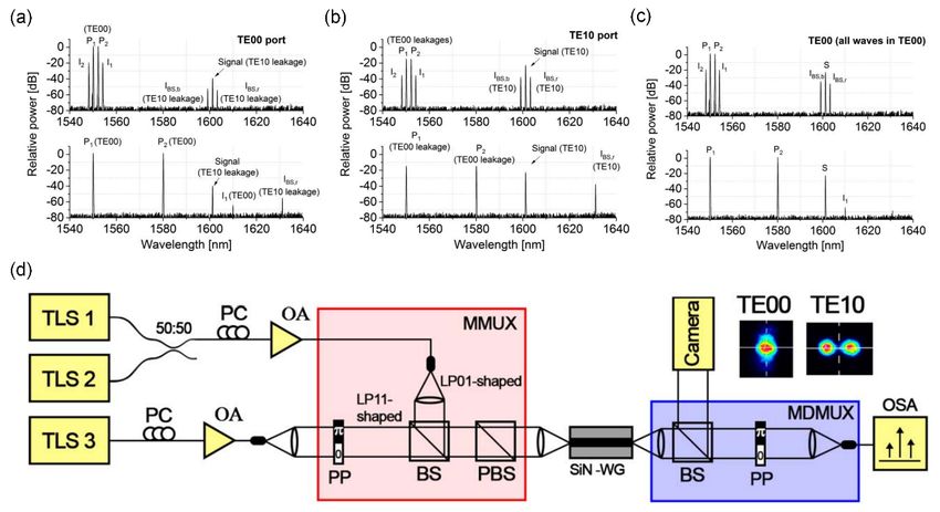
22                                                                                           Kang et al.

window desirable. Soliton pulse pumping in the anomalous dispersion region is usually used for
ultra-broadband SC generation because the associated soliton fission significantly helps the spectrum
broadening. To guarantee a high degree of coherence of spectrum, the pulse width of soliton should
be shortened to hundreds of femtoseconds (better < 100 fs) to construct the scenario of soliton fission
dominating the MI effect. Through reasonable dispersion engineering and pump condition selecting, SC
could cover from UVR to MIR by more than one octave along with high degree of coherence.
      For the generation of Kerr microcomb, high finesse optical microresonator continuously driven by
a continuous-wave (CW) pump laser is typically employed. Although pulse driving methods are also
available, a CW source is sufficient. This is much different from SC generation in straight MNPWs via
injection of pulse with high peak power [58]. Hyper-parametric oscillation (also called cascaded FWM)
arises through Kerr nonlinearity and determines broadband frequency combs generation. By scanning
either pump frequency or cavity resonance to achieve an effective red-detuned condition, multi-states,
e.g., MI, chaotic, and even dissipative Kerr soliton (solitons superimpose on a CW background) states
can be achieved. The stable soliton state is what one desires in Kerr microcombs. In particular, the
single soliton microcomb shows temporally near few-cycle pulse, broadband and smooth hyperbolic
secant shape spectrum in the frequency domain. The coherence of spectrum can be well maintained in
this scenario. Nevertheless, several disadvantages including thermal noise destabilization and difficulties
in fabricating ultrahigh Q-factor microresonators still wait for better solutions.
      In contrast to conventional intramodal FWM that occurs amongst all photons in the same mode,
intermodal FWM occurs among all photons in different modes. While the former one has been
extensively studied, the latter one has been studied rarely. As most materials have normal dispersion
in UVR, VR, or deep MIR, it is impossible to achieve phase matching in these bands for conventional
intramodal FWM. In this sense, intermodal FWM in which phase matching condition among different
modes does not restricted in anomalous dispersion regime is an excellent alternative. Moreover, while the
maximum efficiency of intramodal FWM is achieved near the pump wavelength, the one of intermodal
FWM could be achieved far away from the pump wavelength, meaning a broadband range can be
reached. Intermodal FWM not only has the advantages in phase matching, but also possesses higher
flexibility and better spectral conversion efficiency.

2.1. Supercontinuum and Frequency Comb Generation
Supercontinuum sources are desirable because of their ability in maintaining high spectral brightness in
a broad spectral range. SC is particularly exciting for optical metrology, microscopy, optical frequency
synthesis, optical coherence tomography, molecular spectroscopy, biomedical science, etc. [59].
     Mathematically, SC generation is governed by the generalized nonlinear Schrödinger equation
(GNLSE) under the slow varying envelope approximation. For the operation bands in which the half
band-gap of nonlinear material is below the photon energy, nonlinear multi-photon absorption (MPA)
has to be considered. In addition, for specific semiconductor materials like Si, free carrier induced
attenuation (FCA) and dispersion (FCD) also have to be considered. The modified GNLSE is given
by [60],
                                  1                   iω0 nF CD              1
                                                                          ik+1 βk uT
                                                                                   (k)
                    uz (z, T ) = − (α + αF CA ) u +              u+
                                  2                        c                  k!
                                                                      k≥2

                                          4
                                               1 −(n−1)
                                 + iγ −         A        βnP A |u|2(n−2) × (1 + iτs ∂T )
                                               n eff
                                          n=2
                                             ∞
                                 × u (z, T )     R (t) |u (z, T − t)|2 dt                            (2)
                                            0
where u(z, T ) is the envelope of electric field, α the linear loss, and βk the k-th order dispersion
coefficient related to the Taylor series expansion of propagation constant β(ω) at the center frequency
ω0 . γ is the nonlinear coefficient, τs = 1/ω0 the optical shock time connecting with the self-steepening
effect, and R(t) the Raman response function. Among them, βnP A represents the n-photon absorption
coefficient, and the refractive index changes caused by FCA and FCD are expressed as αF CA = σNc
and nF CD = ζNc , respectively. The free carrier coefficients connected with the waveguide materials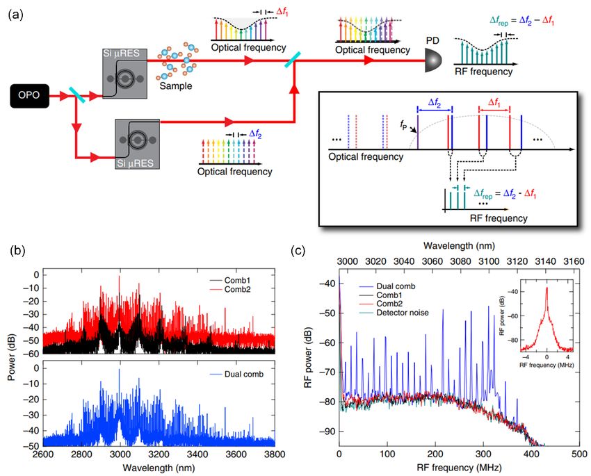
Progress In Electromagnetics Research, Vol. 170, 2021                                                 23

are represented as σ and ζ, and Nc is the free carrier density. The performance of SC is evaluated
by measuring the spectral bandwidth and coherence. Highly coherent SC sources are of significant
interest for precision spectroscopy, high resolution optical tomography, Raman spectroscopy, etc. These
applications demand the low phase fluctuation of spectrum and broad bandwidth. Mathematically, the
interpulse coherence is calculated by [61],

                            (1)                    u∗i (λ, t1 ) uj (λ, t2 )i=j
                           g12 (λ, t1   − t2 ) =                                                     (3)
                                                                2                   2
                                                   |ui (λ, t1 )|     |uj (λ, t2 )|

where u(λ) stands for the amplitude of SC in the frequency domain, and the subscripts i and j represent
the pulses at different time slots of t1 and t2 inside a pulse train, respectively. The expressions in the
angle bracket represent the statistical average of a certain number of shot-to-shot SC pairs with power
and phase noises. Different from the interpulse coherence that describes spectral phase fluctuation of
a pulse train, the recently developed intrapulse coherence provides a method to measure the spectral
phase fluctuation of a single pulse. The intrapulse coherence is given by [62]
                                                2
                                                ui (2λ) u∗i (λ)
                                          Γ=  2                .                                    (4)
                                                ui (2λ) u∗i (λ)
Equation (4) measures the fluctuation of spectral phase difference between a spectral component and
its doubling-frequency counterpart. This intrapulse coherence directly estimates the quality of f − 2f
self-referencing product, which can be used to control the carrier-envelope offset (fCEO ). It has been
numerically proved that a SC source with excellent interpulse coherence might has a poor intrapulse
coherence [63].
      Coherent UVR to VR SC generation has been reported in silica ridge waveguides. Different from
fiber platforms, the silica waveguide arrays provide a wide range of emission wavelength choices on
a single and compact chip. Oh et al. experimentally demonstrated efficient and coherent dispersive
wave generation from UVR to VR in silica waveguides with pumping wavelength of 830 nm [64]. The
waveguide array structure and experimental results are shown in Figure 5.
      Coherent SC generation can be extended from VR to NIR in various nonlinear materials. In
2019, Liu et al. experimentally generated a VR to NIR SC spanning from 600 to 1050 nm in AlN
waveguides [65]. Lafforgue et al. experimentally exploited nitrogen-rich Si3 N4 waveguides to generate
an octave SC spanning from 400 to 1600 nm [66]. Numerical simulations indicated high interpulse
coherence of generated SC. If the pump pulse is shorter than 100 fs [59, 67], generated SC would have
high interpulse coherence. This conclusion has been confirmed by some experiments operating in the NIR
region. For example, Johnson et al. demonstrated the SC generation spanning more than 1.4 octaves in
a Si3 N4 waveguide using sub-100-fs pulses at 1 µm pumping wavelength [68]. A spectral interferometer
was used to verify the high degree of interpulse coherence over the majority of spectral bandwidth. In
2017, Okawachi et al. demonstrated a novel approach to produce coherent and directional SC by using
cascaded dispersive waves [69]. The scheme is achieved by dispersion engineering in Si3 N4 waveguides
pumped at 1050, 1300 and 1400 nm, respectively. By performing direct detection of the carrier-
envelope-offset frequency of femtosecond pump source using an f − 2f interferometer, the coherence
properties of generated SC are experimentally confirmed. Different from previous works conducted on
SiO2 , Si or Si3 N4 platforms, Kuyken et al. recently demonstrated SC generation on the AlGaAs-on-
insulator platform [70]. The pumped wavelength is located at telecom wavelengths (1555 nm). Superior
interpulse coherence within 1450–1750 nm is experimentally validated. Chalcogenide is another suitable
substitute for SC generation in the NIR. For instance, Tremblay et al. fabricated low propagation
loss Ge23 Sb7 S70 waveguides (0.56 dB/cm) in a wafer scale process [71]. By careful engineering of the
waveguide dispersion, coherent and octave-spanning SC pumped at 1.55 µm with picojoule-level energy
is generated. Dave et al. demonstrated the generation of an octave-spanning SC in III-V membrane
waveguides on a Si substrate [72]. The waveguide is pumped by a 1550-nm femtosecond source, and the
generated SC is measured to be highly coherent.
      MIR coherent and broadband SC generation is another hot topic due to its rich application in trace
gas sensing, LIDAR, biomedical imaging, etc. In 2018, Singh et al. demonstrated octave-spanning and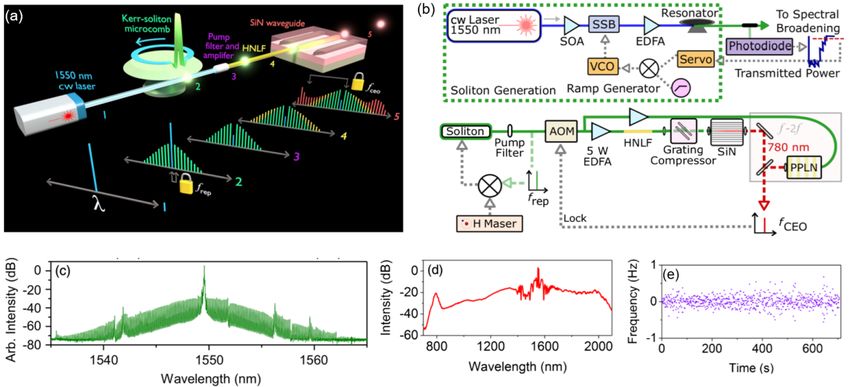
24                                                                                          Kang et al.

            (a)
                                                    (d)

                                                    (e)

            (b)                (c)

Figure 5. Phase matching condition and direct observation of dispersive wave generation in silica ridge
waveguides. (a), (b) SEM images of an array of silica ridge waveguides on a Si chip. The red box in
(a) contains a silica waveguide whose cross section is shown in (b); the cross section is superimposed
with the calculated mode profile of the TM mode at a wavelength of 830nm. (c) Calculated mode area
and zero dispersion wavelength are plotted as the ridge base width varies. (d) Calculated GVD (dashed
lines) and phase-matching parameter (solid lines) for dispersive wave generation in TM polarization are
plotted as the wavelength varies. Blue, red, and yellow solid and dashed lines correspond to mode areas
of 0.83, 1.03, 1.69 mm2 , respectively. (e) UVR-VR dispersive wave generation in a Si chip containing
an array of waveguides with varying mode area [64]. Copyright 2017 Nature Publishing Group.

coherent SC generation in SOI from 1.06 µm to beyond 2.4 µm [73]. The coherence of generated SC is
measured to be more than an octave. Suspended waveguide structures are promising for deep-MIR SC
generation because there is an air gap as the buffer layer between light-guiding region and substrate.
As a result, strong mode confinement eliminates mode-leaking loss, and the limitation of transparency
window caused by substrate material can be overcome. So far, suspended MNPWs on several material
platforms with air gap have been fabricated and utilized for deep-MIR SC generation. For example,
Kou et al. experimentally used a suspended rib Si waveguide to achieve a broadband SC spanning from
2 to 5 µm in 2018 [74]. Chiles et al. demonstrated a 2.3 ∼ 6.5 µm broadband SC by using a suspended
AlGaAs waveguide [75] in 2019. At the same year, Nader et al. achieved an ultra-broadband SC spanning
from 2 to 8 µm by using a suspended Si waveguide [76]. The deeply extended SC source was successfully
utilized for on-chip dual comb spectroscopy. Figure 6 shows several fabricated suspended platforms for
deep-MIR SC generation. MIR SC generation on MNPWs that are not suspended was also reported.
The spectral extension in this scenario is mainly limited by the transparency of the substrate. In
2014, Lau et al. experimentally demonstrated coherent octave-spanning MIR SC generation in Si-based
MNPWs [77]. They also numerically showed that MPA and FCA are not detrimental to SC generation
in the MIR region. In 2016, Xie et al. demonstrated a more than 1.5 octave-spanning and coherent
MIR SC covering 1.5 to 3.6 µm by pumping a so-called As2 S3 -silica “double-nanospike” waveguide [78].
In 2018, Sinobad et al. demonstrated an octave SC generation on a Si0.6 Ge0.4 waveguide [79]. The
spectrum of the SC generated covered from 3 to 8.5 µm, almost reaching the limit of Si transparency.
In 2019, Sinobad et al. demonstrated coherent and an octave-spanning broad MIR SC generation on
an air-cladded SiGe-on-Si waveguide [80]. At the extreme ends of spectrum, high spectral density and
coherence can be obtained after dispersion engineering. Theoretical works also contributed to the design
and manipulation of deep-MIR SC generation targeted at suspended MNPWs. For example, Yang et
al. numerically utilized 700-fs pump pulses with a low peak power of 400 W to pump a suspended Ge-
on-Si waveguide at 6.57 µm wavelength [81]. The SC generated was confirmed to span from 2 to 12 µm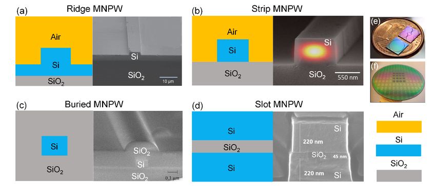
Progress In Electromagnetics Research, Vol. 170, 2021                                                25

                     (a)                  (b)                     (c)

                      (d)

Figure 6. (a) (b) (c) SEM images of suspended waveguides from [74–76], respectively. (d) SCs when
the pump wavelength is 3060 nm, experimentally measured spectra with different waveguide-coupled
pulse energies (solid curves), and simulated spectrum at 45 pJ waveguide-coupled pulse energy (dotted
curve), with a trace-to-trace offset of 30 dB [75]. Copyright 2018 & 2019 OSA.

with excellent coherence in the whole spectrum range. In 2017, Yuan et al. numerically studied SC
generation in a 4-mm-long suspended Ge-membrane ridge waveguide pumped by a 180-fs pulse of peak
power of 800 W and central wavelength of 4.8 µm [82]. Generation of coherent and ultra-broadband
MIR SC spanning from 1.96 to 12 µm is studied. In 2018, Jing et al. numerically studied coherent
and broadband SC generation in a 3.1-mm-long suspended As2 S3 ridge waveguide pumped by a pulse
source with a peak power of 450 W [83]. The generated SC covers from 1.0 to 5.6 µm. In 2019, Cheng
et al. numerically studied the combination of self-similar PC and coherent SC generation in a specially
designed suspended Si waveguide tapers [84]. Simulation results showed that a 1-ps pulse was perfectly
compressed to 47.06 fs first, and then used for highly coherent and broadband MIR SC generation. In
2019, Li et al. numerically studied multi-octave MIR SC and frequency comb generation in a suspended
As2 Se3 ridge waveguide [85]. The generated SC spectrum could cover 1.76 ∼ 14.42 µm (more than three
octaves) and had excellent coherence. In 2020, Lai et al. numerically designed a T-type Ge waveguide
with the all-normal dispersion profile for MIR SC and frequency comb generation [86].
     Some recent works show that ultrabroad SC that covers multi-bands from UVR to MIR can be
generated by dispersive wave assistance in specially designed MNPWs. In 2019, Yu et al. experimentally
demonstrated coherent two-octave SC generation covering 400 ∼ 2400 nm in a 0.5-cm-long x-cut nano-
LiNbO3 waveguide with only 100-picojoule-level pump energy [87]. This system also supports SHG
generation at 750 nm, which enables directly f − 2f self-referencing detection on single waveguide. In
2020, Lu et al. experimentally demonstrated ultra-broadband SC generation from UVR to MIR in single-
crystalline AlN waveguides [88]. Subsequent numerical simulations indicated a high degree of coherence
of generated SC around the telecom pump and two dispersive waves. The reported SC generation on
different platforms in the new bands are summarized in Figure 7. We note the suspended structures are
promising for MIR SC generation, especially in the deep MIR region (> 4 µm). This is because not only
the loss induced by the mode-leakage is eliminated, but also the core-cladding refractive index contrast
is enhanced which leads to smaller mode area and stronger nonlinear interaction. The core layer of a
suspended waveguide is typically a ridge structure, which enables array of holes on the ridge arms for
wet-etching of substrate. A core layer of strip structure is also feasible because the suspension can be
fabricated as pillar structure. The slot and multi-layer hybrid structures generally lead to flattened
26                                                                                            Kang et al.

Figure 7. Reported SC generation on different platforms in the new bands. The grey dashed lines
indicate the transparent windows of different materials. Experimental studies are marked with ‘*’.

dispersion with multiple zero-dispersion wavelengths, which is beneficial to broadband SC generation.
     Optical frequency comb refers to a coherent source composed of discrete frequency lines with equal
frequency interval. Frequency comb sources have found many applications in the fields of metrology,
optical, atomic clocks, and high precision spectroscopy. While traditional laser-based frequency comb
can be highly coherent, the spectral width is restricted by the gain bandwidth and is rather narrow.
SC relates to frequency comb due to the development of f − 2f self-referencing technique. The fCEO of
a frequency comb can be detected and locked by this technique when the spectrum is octave spanning.
This is crucial because most applications like metrology and spectroscopy require absolute frequency
accuracy. Pumped by a repetition-rate (frep ) stabilized femtosecond pulse train, the generated SC
can be seen as a broad frequency comb with comb line interval equaling to frep . The fCEO of
generated octave-spanning SC can be locked by f − 2f technique, which makes SC an ultra-broadband
frequency comb source. Experimental results of SC-based optical frequency combs on MNPWs have also
been reported. Kuyken et al. experimentally demonstrated an octave-spanning MIR frequency comb
generated on a Si nanowire waveguide [108]. The phase-coherent frequency comb was generated with
a −30 dB spectrum spanning from 1540 up to 3200 nm, and with coupled pump pulse energy as low
as 16 pJ. Carlson et al. demonstrated self-referenced and efficient frequency comb on Si3 N4 waveguide.
Compared with conventional approaches that using highly nonlinear fibers, the average power is found
to be approximately 10 fold lower [109]. Lee et al. experimentally achieved coherent SC generation in
a nanospike chalcogenide-silica hybrid waveguide with pump pulse at 2 µm wavelength. The generated
SC enables coherent locking of OPO to the optically referenced pump frequency comb, which results in
a composite frequency comb with spectrum spanning 1 ∼ 6 µm [110].
     Dispersive wave generation is another efficient method to achieve broadband optical frequency comb
in new bands. Dispersive waves are less technologically flexible but more easily achieved than SC, as long
as the perturbation of high-order dispersion is considerable. The spectrum of dispersive wave is localized
and directional, which avoids energy waste in unwanted frequencies. The central frequency as well as the
conversion efficiency of dispersive wave is tunable by tailoring the dispersion of waveguides. Of note, the
coherence of pump source can be perfectly inherited by dispersive wave regardless of noise perturbation.
Experimentally, in 2018, Guo et al. used a Si3 N4 nanowire pumped by a 1.55 µm erbium-doped fiber-
based femtosecond laser frequency comb to directly generate a MIR dispersive wave frequency comb
Progress In Electromagnetics Research, Vol. 170, 2021 27
(a)
(b)
(c) (d)
Figure 8. (a) Schematic diagram of the MIR dual-comb gas-phase spectroscopy, in which two
MIR frequency combs are generated via coherent supercontinuum process in nanophotonic chip-based
Si3 N4 waveguides, seeded by a mutually locked dual-frequency-comb source at the telecom-band (i.e.,
∼ 1550 nm). HWP, half-wave plate; PD, (MIR) photodetector. (b) Microscopic pictures of a photonic
chip with coupled Si3 N4 waveguides, corresponding to both the input section, where the beginning
of the waveguide contains an inverse taper structure, and the output section has dual-core waveguide
structures. The false-colored SEM image of the waveguide cross section is also presented. (c) Calculated
effective refractive indices of symmetric (purple curve) and anti-symmetric (orange curve) modes in
a dual-core Si3 N4 waveguide, compared with initial uncoupled modes separated in each core. (d)
Experimentally observed supercontinuum generation in a dual-core Si3 N4 waveguide [112]. Copyright
2020 OSA.
covering from 2.5 to 4 µm [111]. To realize the phase match between dispersive and pump waves, the
integrated dispersion βint should be zero. However, it is a little regretful that the conversion efficiency
was only around 1%. In 2020, the same group experimentally obtained MIR dual-comb spectroscopy
based on dispersive wave generation in dual-core Si3 N4 nanowires [112]. Figure 8 shows the schematic
diagram of the MIR dual-comb spectroscopy, the microscopic and SEM pictures of the dual-core Si3 N4
waveguide, and the experimental results of the MIR dispersive wave. Two fully stabilized femtosecond
laser frequency combs (Menlo comb system, frep ∼ 250 MHz) with slight repetition rate difference
(Δfrep ≈ 320 Hz) were used as the two pump seeds. The bandwidth of their dual-comb spectrometer28 Kang et al.
covers the functional group region from 2800 to 3600 cm−1 , including more than 100,000 comb lines.
The excellent performance enables quick and parallel gas-phase detection with a high sensitivity and
sub-Doppler spectral resolution. In 2019, Grassani et al. experimentally demonstrated MIR dispersive
wave tunable within 3 ∼ 4 µm by pumping the specially designed “top-hat” Si3 N4 nanowires with a
2 µm fiber laser source [113]. A record-high conversion efficiency of 35% was achieved. The MIR source
generated was successfully used for detection of C2 H2 by absorption spectroscopy. On the same Si3 N4
platform, in 2020, Tagkoudi et al. experimentally broadened the reachable spectral range of dispersive
wave through careful optimization [114]. As a result, the dispersive wave can span the entire 3 ∼ 3.5 µm
window without losing conversion efficiency. Table 1 summarizes the optical characteristics of different
materials for chip-scale platform as a comparison.
Table 1. Optical characteristics of different materials for chip-scale platform.
Bandgap βT P A (m/W) β3P A (m3 /W2 ) n2
Material n α (dB/cm) Refs.
(eV) & cut-off λ & cut-off λ (m2 /W)
2 × 10⁻²⁷
5 × 10⁻¹²
Si 1.1 (@2.6 µm) 3.47 6 × 10⁻¹⁸ 3.4 [89–91]
& 2.2 µm
& 4.3 µm
7 × 10⁻¹²
a-Si:H 1.7 / 3.73 1.7 × 10⁻¹⁷ 2.1 [89, 92]
& 2.15 µm
6 × 10⁻¹⁰ 5 × 10⁻²⁷
4.3 (@ 4.4 × 10⁻¹⁷
Ge 0.8 (@2.8 µm) (@4.8 µm) 2 [89, 90]
3.2 µm) (@3.2 µm)
& 2.83 µm & 5.2 µm
5 × 10⁻¹² 2 × 10⁻²⁷
1.5 × 10⁻¹⁸
Si0.6 Ge0.4 1.0 (@2.05 µm) (@3.2 µm) 3.59 1.1 (@4 µm) [90, 93]
(@4 µm)
& 2.4 µm & 4.3 µm
SiO2 9.0 / / 1.46 2.6 × 10⁻²⁰ / [94]
Si3 N4 5.3 / / 1.98 2.5 × 10⁻¹⁹ 0.5 [95, 96]
SiC 3.26 / / 2.6 8 × 10⁻¹⁸ 12.8 [97]
AlN 6.2 / / 2.1 2.3 × 10⁻¹⁹ 0.6 [98]
Ta2 O5 4.4 / / 2.05 7.2 × 10⁻¹⁹ 1.5 [99]
TiO2 3.1 / / 2.4 3.6 × 10⁻¹⁸ 5 [100]
Diamond 5.5 / / 2.4 8.2 × 10⁻²⁰ 0.34 [101]
−13 −17
AlGaAs 1.72 5 × 10 / 3.3 2.6 × 10 1.3 [102, 103]
LiNbO3 3.8 / / 2.21 2.5 × 10⁻¹⁹ 0.027 [89, 104]
−15 −18
As2 S3 2.26 6.2 × 10 / 2.43 3.8 × 10 0.05 [89, 160]
As2 Se3 1.77 1.4 × 10⁻¹² / 2.81 2.4 × 10⁻¹⁷ 1.4 [105, 106]
Doped silica / / / 1.7 1.15 × 10⁻¹⁹ 0.06 [89, 107]
Note: The parameters without specification are values at 1.55 µm.
2.2. Kerr Microcombs Generation
Generation of Kerr microcombs on chip-scale optical microresonators is a robust and competitive
technique for coherent sources generation in the new bands. It facilitates ultra-compact size to satisfy
out-of-the-lab applications and shows explosive development in the last decade. Microresonators made
of χ(3) nonlinear materials, such as silica, highly doped silica, Si3 N4 , MgF2 , AlN [115], etc. can have high
quality factor. Although Kerr microcombs generation has revolutionized the fields in the near-infrared
band, such as terabit optical coherent communication, dual-comb spectroscopy, ultrafast ranging, atomic
clocks, optical synthesis, etc. [116], it is still not widely developed in MIR, UVR, and VR bands.Progress In Electromagnetics Research, Vol. 170, 2021 29
When a CW pump field uin with a center frequency of ω0 is coherently injected into the cavity
through a coupler, the boundary condition of the intracavity field uin at the beginning of m + 1 round
trip is related to that at the end of the m round trip, which is described by the iteration step of Ikeda
map as [117, 118],
1 1
um+1 (0, T ) = θ 2 uin + (1 − θ) 2 um (L, T ) eiφ0 (5)
where T represents the retarded time scale in one roundtrip, θ the power coupling coefficient of coupler,
L the roundtrip length of cavity, and φ0 the linear phase accumulation of the field inside the cavity per
roundtrip. In each roundtrip, the evolution of u(z, T ) |L
z=0 is obtained by a GNLSE governed propagation
model, as given by,
1 1
ik βk uT + iγ (1 + iτs ∂T ) |u|2 u
(k)
u (z, T )z = − αu + i (6)
2 k!
k≥2
where z indicates the propagation distance, and τs indicates the optical shock time. For high finesse
resonators, Eqs. (5) and (6) can be averaged to a mean-field Lugiato-Lefever equation (LLE) [119],
⎡ ⎤
1 1 1
tR ut (t, T ) = θ 2 uin − (αL + θ) u + i ⎣L ik βk ∂T + γL (1 + iτs ∂T ) |u|2 − δ0 ⎦ u
(k)
(7)
2 k!
k≥2
where tR stands for the round-trip time, and t represents the slow time variable. Strictly, this equation
is only valid when t is equal to an integer multiple of tR . The fast time T scales for the duration of
temporal waveform in the resonator. The phase detuning of pump field with respect to the closest
resonance peak with order l is expressed as the cavity phase detuning δ0 = 2πl − φ0 . In addition, if
the microresonator is made of materials like Si, the general LLE should be modified to include the free
carrier and multi-photon absorption effects [120, 121],
⎡ ⎤
ik
1 1 1 αF CA i
αL + θ + iδ0 u + ⎣iL + ω0 nF CD ⎦ u
(k)
tR ut (t, T ) = θ 2 uin − βk ∂T −
2 2 k! 2 c
k≥2
4
1 −(n−1)
+ iγL − L Aeff βnP A |u|2(n−2) × (1 + iτs ∂T )
n
n=2
⎡ ⎤
∞
× ⎣u (t, T ) R (η) |u (t, T − η)|2 dη ⎦ (8)
0
For Kerr microcombs generation in the VR region, in 2014, Jung et al. experimentally proposed a method
with high-Q AlN microring resonator pumped by a telecom CW laser [115]. The Kerr microcomb at
the telecom band was generated first, and then used to generate comb-like spectrum at the VR region
through the second harmonic, third harmonic, and sum frequency conversion in the same AlN microring.
Similarly, in 2018, Liu et al. experimentally utilized an AlN microring to obtain near-VR comb lines in
720 ∼ 840 nm from a NIR microcombs through spectral translation [122]. The conversion efficiency is
as low as 4.1 × 10⁻⁵ %. In 2016, Wang et al. experimentally demonstrated green-light frequency comb
generation in high-Q Si3 N4 microring resonators with a conversion efficiency of only 0.04% [123]. The
nonlinear processes in this experiment involve third harmonic generation and third-order sum frequency
generation, which allows the conversion of NIR frequency combs into green light region. By using a high-
Q AlN microring, Guo et al. achieved near VR region Kerr microcombs in 2018 with a high conversion
efficiency of 22% [124].
In the NIR region, silica and Si3 N4 are the most efficient materials for chip-scale Kerr microcomb
generation. For example, Si3 N4 simultaneously possesses relative high Kerr nonlinearity (typically
∼ 0.9 W−1 /m), low loss (typically ∼ 0.2 dB/cm), no photon-absorption, and mature fabrication
technology compatible with the CMOS foundry. In 2017, Lee et al. experimentally achieved soliton
microcombs around 778 and 1064 nm with an on-chip high-Q silica edge microresonator [125]. In30 Kang et al.
2019, Raja et al. experimentally coupled an III-V-material-based laser diode chip to a high-Q Si3 N4
microresonator [126]. With an average power less than 1 W, a soliton microcomb with sub-100-GHz line
spacing has been obtained with pump wavelength around 1540 nm. In 2020, Briles et al. experimentally
utilized the Si3 N4 microresonators to comprehensively study low-power octave-spanning single soliton
Kerr microcombs generation in both the 1550 nm and 1064 nm bands [127]. In the same year, Fujii et
al. experimentally demonstrated that by engineering the sidewall angle of a small-radius (∼ 100 µm),
3-µm-thick silica wedge microdisk, dispersion tuning in both normal and anomalous regimes can be
realized without significantly affecting the free spectral range [128]. The designed microdisk with a
wedge angle of 55◦ was used to generate a 300 nm wide Kerr microcomb in the anomalous dispersion
region under pump wavelength around 1550 nm.
In the MIR region, Group IV elements are employed to fabricate the microresonators because their
broad transparent windows and negligible nonlinear photon-absorptions in this region. Silicon-based
or germanium-based microresonators are promising platforms for MIR Kerr microcombs generation.
In 2016, Yu et al. experimentally generated a mode-locked soliton Kerr microcomb in the MIR region
covering the spectral range from 2.4 to 4.3 µm [129]. It was found that up to 40% of pump energy
was converted to the output comb power. Two years later, in 2018, the same group experimentally
demonstrated MIR dual-comb spectroscopy on a SOI microring platform [130]. Figure 9 shows the
experimental setup, dual-comb generation, and dual-comb spectroscopy results. A single CW pump
source with power as low as 80 mW was used to generate two coherent Kerr microcombs covering
2.6 ∼ 4.1 µm in two Si microrings with slightly different free spectral range (FSR). The pump-to-comb
conversion efficiencies of two microcombs are found to be both > 30%. Although the microcombs
generated are multi-soliton state, the dual-comb spectroscopy could still acquire spectra of acetone at
127 GHz (4.2 cm−1 ) resolution. They further demonstrated high-throughput label-free MIR dual-comb
(a)
(b) (c)
Figure 9. (a) Experimental setup for dual-comb absorption spectroscopy. (b) Spectra of each mode-
locked comb (multi-soliton states) and combined M-FT spectrum. (c) RF spectrum from the dual-comb
interferometer [130]. Copyright 2018 Nature Publishing Group.Progress In Electromagnetics Research, Vol. 170, 2021 31
spectroscopy based on Kerr microcombs in Si microfluidic microresonators. The label-free spectroscopy
gives a direct detection of targeted molecular regardless of fluorescent labeling. The flow dynamics of
an acetone droplet was successfully measured with a high spectral acquisition rate of 25 kHz (40 µs per
spectrum, comparable to the state-of-art Michelson based Fourier-transform infrared spectrometer)
covering a spectral range from 2900 to 2990 nm [131]. The mitigation of intracavity stimulated
Raman scattering when the pump wavelength is shifted to 2 µm band eliminates the Raman–Kerr
comb competition, thus facilitating soliton microcombs generation. Gong et al. experimentally generate
microcombs around 2 µm in a high-Q z-cut nano-LiNbO3 microring [132]. This is the first experimental
demonstration of MIR single soliton Kerr microcomb generation on nano-LiNbO3 platform.
In the respect of theoretical works, in 2018, Guo et al. numerically obtained an octave-spanning
Kerr microcombs in a germanium (Ge) microresonator covered from 2.3 to 10.2 µm [133]. The spectral
bandwidth and flatness were remarkably enhanced by maintaining dispersion flatness from 3.5 to 10 µm
through a mode hybridization technique. The mode hybridization gives abruptly inflection of dispersion
profile at the hybridization wavelength, and thus leads to transformation between normal and anomalous
dispersion regimes. New nonlinear platforms have been proposed for MIR Kerr microcombs generation.
In 2019, Fan et al. numerically showed that a slot waveguide could obtain mode-locked MIR Kerr
microcomb in a LiNbO3 microring [134]. With only 50 mW pump power, the generated Kerr microcomb
covers from 2810 nm to 4630 nm. In 2019, Anashkina et al. numerically studied MIR Kerr microcomb
generation spanning 3 ∼ 4 µm at −30 dB spectrum level in an As2 S3 microbubble resonator with a
potential low pump power of 10 mW [135]. The spectral range of the Kerr microcombs could span
more than 700 nm. An effective method for spectrum stretching of Kerr microcombs is to draw support
from a post process of SC generation. In this method, a CW source is used as primary pump to
generate the Kerr microcomb in a microresonator. The generated Kerr microcomb is filtered to remove
the residual CW pump component, and then injected into a strip waveguide for SC generation. The
generated broadband SC is used for f − 2f self-referencing locking of carrier-envelope phase. This
idea has been experimentally achieved by Lamb et al. in 2018. A broadband, 15-GHz repetition-rate
frequency comb source is achieved, which is appropriate for optical-frequency comparisons and f − 2f
self-referencing [136]. The principle, experimental setup, and results for soliton Kerr microcomb and
SC generation are shown in Figure 10. Table 2 summarizes the reported schemes for Kerr microcomb
generation at VR, NIR, and MIR bands.
Table 2. Reported Kerr microcombs generation in the new bands. Experimental studies are marked
with ‘*’.
Region Material Structure Q factor Range (µm) Refs.
5
VR AlN Microring QL : 5 × 10 0.517, 0.776, and 1.4 to 1.65 [115]*
VR and NIR AlN Microring QL : 1.1 × 10⁶ 0.72 to 0.84, and 1.4 to 1.7 [122]*
VR and NIR SiN Microring QL : 1.30 × 10⁶ 0.502 to 0.58, and 1.327 to 2.082 [123]*
VR and NIR AlN Microring / 0.72 to 0.82, and 1.4 to 1.7 [124]*
VR and NIR SiO2 Microring Q0 : 8 × 10⁷ 0.76 to 0.79 [125]*
NIR Si3 N4 Microring Q0 > 1 × 10⁷ 1.5 to 1.56 [126]*
NIR LiNbO3 Microring QL : 1.1 × 10⁶ 1.68 to 1.8, and 1.88 to 1.96 [132]*
NIR Si3 N4 Microring / 1.1 to 2.4, and 0.86 to 1.7 [127]*
NIR SiO2 Microdisk QL : 4.5 × 10⁵ 1.4 to 1.7 [128]*
MIR Si Microring QL : 2.45 × 10⁵ 2.4 to 4.3 [129]*
MIR Si Microring Q: 1 × 10⁵ 2.6 to 4.1 [130]*
MIR Si Microring / 2.9 to 2.99 [131]*
MIR Ge Microring Q0 : 4 × 10⁴ 2.3 to 10.2 [133]
MIR LiNbO3 Microring / 2.81 to 4.63 [134]
MIR As2 S3 Microbubble Q0 : 1 × 10⁶ 3 to 4 [135]
VR to MIR Silica+Si3 N4 Microdisk + strip / 0.7 to 2.1 [136]*32 Kang et al.
(a) (b)
(c) (d) (e)
Figure 10. (a) Pictorial representation of frequency-comb generation and spectral evolution through
the system. A two-stage approach, first using a highly nonlinear fiber (HNLF) and then using a
S3 iN4 waveguide, is used to achieve broadband spectra from a microcomb. (b) Upper panel: soliton
generation and stabilization using the lock technique described in the text. cw, continuous wave; SOA,
semiconductor optical amplifier; SSB, single-side band modulator; EDFA, erbium-doped fiber amplifier;
VCO, voltage-controlled oscillator. Lower panel: SC generation and frequency-comb stabilization with
a S3 iN4 waveguide. frep, repetition-rate frequency; AOM, acousto-optic modulator; HNLF, highly
nonlinear fiber; SiN, silicon nitride; PPLN, periodically poled lithium niobate; fCEO , carrier-envelope
offset frequency. (c) Spectrum of a single soliton. (d) Octave-spanning SC generated when the waveguide
is pumped with a single soliton. (e) Frequency-counter data for the locked fCEO (1 s gate time) [136].
Copyright 2018 APS.
2.3. Intermodal Four-Wave Mixing
Conventional FWM involves four optical waves (nondegenerate) or three optical waves (degenerate) in
a nonlinear medium. For example, in the process of degenerate FWM two pump photons at frequency
ωp are converted into another two photons with new frequencies ωs and ωi, satisfying 2ωp = ωs + ωi, .
This process obeys the energy and momentum conservation. The efficiency η of FWM can be written
as [137]:
L 2
η ∝ sin c Δk (9)
2π
where Δk represents the phase matching, and L stands for the length of waveguide. The phase
matching condition means Δk should be zero to maximize the efficiency. Δk includes a linear part
ΔkL and a nonlinear part ΔkN L , which are related to the waveguide modes of the pumps, signal
and idle. Intermodal FWM requires phase matching among different guided modes. Considering the
nondegenerate FWM process, the linear part ΔkL determined by the effective refractive index neff is
given by [137],
ωp1 j ωp2 q ωs ωi
ΔkL = neff (ωp1 ) + neff (ωp2 ) − nleff (ωs ) − nm (ωi ) (10)
c c c c eff
where p1 , p2 , s, i represent two pumps, signal, and idle, respectively; c is the velocity of light in vacuum;
j, q, l, m indicate the orders of guided modes of the first pump, the second pump, the signal, and the
idler photon, respectively.
In recent years, intermodal FWM has been preliminarily studied on Si-based MNPWs. In 2018,
Signorini et al. studied both the intermodal spontaneous and stimulated FWM through simulation
and experiment [137]. The geometrical parameters of waveguide enabled flexible dispersion engineering
so that phase matching conditions among different modes could be satisfied. Figure 11 shows theProgress In Electromagnetics Research, Vol. 170, 2021 33
(a)
(b) (c)
Figure 11. (a) Setup for the stimulated FWM. The pump is initially filtered with two 1550 nm bandpass
filters. Then, the pump and signal are mixed by a free-space beam splitter and coupled into the same
tapered lensed fiber through a collimator. The input fiber injects the light into the waveguide on the
SOI chip. The light is collected from the waveguide by another tapered lensed fiber. The collected
light is analyzed with an OSA or a monochromator. In the inset, the waveguide modes are sketched by
showing the mode profiles; as an example, the case of the (1, 2, 2, 1) modal combination is considered.
For the spontaneous FWM, the setup is the same except for the lack of the input signal. (b) Spectrum
of the stimulated FWM with the (1, 2, 2, 1) TE intermodal combination. The stimulating CW signal at
1640 nm is converted into the pulsed idler at 1469 nm. The smaller peaks are spurious signals due to the
OSA. (c) Spectrum of the stimulated idler generation efficiency with the intermodal FWM combination
(1, 2, 2, 1) TE mode. The blue circles are the measured data, while the orange line is the simulation. The
simulated spectrum was shifted by −3.3 dBm in order to match the experimental data [137]. Copyright
2018 OSA.
experimental setup and intermodal FWM results. When the pump was on both the fundamental and
2-nd TE modes, and the signal was on the fundamental TE mode, an idler on the 2-nd TE mode was
achieved. They also studied intermodal FWM with other modal combinations up to 3-rd TE and TM
modes.
In the same year, Signorini et al. achieved single photon pairs through the intermodal FWM on
a Si rib waveguide. The coincidences between the idle at 1.281 µm and the signal at 1.952 µm with
the (1, 2, 2, 1) TE modal combination were measured [138]. They proposed asymmetric directional
couplers to extract higher-order modes, demonstrating a fully integrated scheme of intermodal FWM.
The high tunability of phase matching wavelength and bandwidth of intermodal FWM was studied
in their work. In 2019, Lacava et al. used the Bragg scattering (BS) intermodal FWM method to
achieve a dual-CW-pumped SOI wavelength converter [139]. The idler and signal were both on the
fundamental TE mode, and two pumps were on the 2-nd TE mode. They found that the overall BS
FWM efficiency was limited by the TPA and FCA effects in Si. In the same year, they also proposed
another scheme to realize the BS intermodal nondegenerate FWM on a fabricated Si-rich silicon nitride
platform [140]. Figure 12 shows the experimental setup in this work. The two pump waves on the
fundamental mode are in the C-band and could realize efficient phase matching with the signal on the
2-nd TE mode far away in the L-band. Thus, the wavelength conversion over a bandwidth exceeding
40 nm was achieved by intermodal FWM. The conversion efficiency (ratio between the output idler and
the output signal power levels) was measured to be −15 dB for a total input pump power of 32 dBm.You can also read