OIF Next Generation Interconnect Framework - OIF-FD-Client-400G/1T-01.0 April 2013
←
→
Page content transcription
If your browser does not render page correctly, please read the page content below
OIF Next Generation Interconnect
                Framework

                  OIF-FD-Client-400G/1T-01.0

                           April 2013

www.oiforum.com                                1
Abstract:
As the OIF looks forward to the higher data rates and/or higher throughput that will be required for
the next generation of systems, a consensus has been reached that new technologies will be
required. This framework document represents the efforts of the OIF to identify the hardware
interconnection application spaces where the communications industry might benefit from
interconnection definitions or “Implementation Agreements” (IA). The objective of this paper is to
identify key technical challenges for next generation systems, define optical and electrical
interconnection applications and discuss some of the interoperability test challenges so that the
OIF and other industry bodies will have a common language as well as understanding of the
development projects that are required for the next generation data rate systems.

Next Generation Interconnect Framework Contributors:

Document Co‐Editors:
Nathan Tracy                     TE Connectivity
Torsten Wuth                     Nokia Siemens Networks

Individual Clause Editors:
Robert Brunner (Clause 2)        Ericsson
Graeme Boyd (Clause 3)           PMC Sierra
Tom Palkert (Clause 4)           Molex
Brice Achkir (Clause 5)          Cisco
Ali Ghiasi (Clause 5)            Broadcom

Along with the many members of the OIF who provided their inputs to this document.

The OIF is an international non profit organization with over 100 member companies, including
the world’s leading carriers and vendors. Being an industry group uniting representatives of the
data and optical worlds, OIF’s purpose is to accelerate the deployment of interoperable, cost-
effective and robust optical internetworks and their associated technologies. Optical internetworks
are data networks composed of routers and data switches interconnected by optical networking
elements.

With the goal of promoting worldwide compatibility of optical internetworking products, the OIF
actively supports and extends the work of national and international standards bodies. Formal
liaisons have been established with The ATM Forum, IEEE 802.3, IETF, ITU-T Study Group 13,
ITU-T Study Group 15, MEF, NPF, T1M1, T1X1, TMF, UXPi and the XFP MSA Group.
                                For additional information contact:
                   The Optical Internetworking Forum, 39355 California Street,
                                  Suite 307, Fremont, CA 94538
                               510-608-5928 Φ info@oiforum.com
                                        www.oiforum.com

   www.oiforum.com                                                                                 2
Table of Contents
Contents
Glossary† ......................................................................................................................................... 5
1 Executive Summary ................................................................................................................. 7
2 Introduction ............................................................................................................................... 8
2.1 Purpose ............................................................................................................................. 8
2.2 Motivation .......................................................................................................................... 9
2.2.1 Challenges of Power Dissipation ............................................................................. 12
2.2.2 Challenges of I/O Densities on Chips and Connectors ........................................... 12
2.2.3 Challenges of Channel Characteristics.................................................................... 13
2.2.4 Challenges of Electrical Link Reach ........................................................................ 13
2.3 Summary ......................................................................................................................... 14
3 Interconnect Applications ....................................................................................................... 15
3.1 Die to Die Interconnect Within A Package ...................................................................... 15
3.2 Die to optical engine within a package............................................................................ 16
3.3 Chip to Nearby Optical Engine ........................................................................................ 16
3.4 Chip to Module ................................................................................................................ 17
3.5 Chip to Chip within PCBA ............................................................................................... 17
3.6 PCBA to PCBA across a Backplane/Midplane ............................................................... 18
3.7 Chassis to Chassis within a Rack ................................................................................... 19
3.8 Rack to Rack side-by-side .............................................................................................. 19
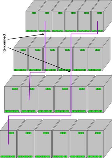
3.9 Rack to Rack in the same row ........................................................................................ 20
3.10 Rack to Rack in the same building .............................................................................. 21
3.11 Rack to Rack in the same data warehouse ................................................................. 22
3.12 Rack to Rack in the same campus .............................................................................. 23
3.13 Longer than 2km links ................................................................................................. 23
3.14 Interconnect Application Summary.............................................................................. 23
4 Points of Interoperability ......................................................................................................... 25
4.1 Electrical Channel points of interoperability .................................................................... 25
4.1.1 Die to Die, Chip to Chip, Back/Midplane, Chip to Optical engine interconnects ..... 25
4.1.2 Chip to module interoperability points...................................................................... 27
5 Opportunities for Future Work ................................................................................................ 29
5.1 Introduction ..................................................................................................................... 29
5.2 Electrical Interconnect ..................................................................................................... 29
5.2.1 Electrical Connectors ............................................................................................... 29
5.2.2 Electrical Links ......................................................................................................... 29
5.3 Optical Interconnect ........................................................................................................ 30
5.3.1 Optical Connectors .................................................................................................. 30
5.3.2 Optical Links ............................................................................................................ 30
5.4 Thermal Management ..................................................................................................... 31
6 Relation to Other Standards ................................................................................................... 32
7 Summary ................................................................................................................................ 33
List of Tables
Table 1 Forward Looking Optical 40Tbps Scenarios .................................................................. 10
Table 2 Intra-Interconnect Applications ....................................................................................... 23
Table 3 Inter-Interconnect Applications ....................................................................................... 24
www.oiforum.com 3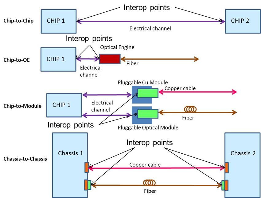
List of Figures
Figure 1 Interconnect Application Spaces ..................................................................................... 8
Figure 2 Scaling Gates/Bumps/Pins (Ref. Xilinx, I/O Line Added) .............................................. 11
Figure 3 Next Generation Interconnect Challenges ..................................................................... 11
Figure 4 Interconnect Application Spaces .................................................................................... 15
Figure 5 Die to Die within an MCM Interconnect Application Space ............................................ 15
Figure 6 Die to Optical Engine MCM Interconnect Application Space ......................................... 16
Figure 7 Chip to nearby OE Interconnect Application Space ....................................................... 16
Figure 8 Chip to Module Interconnect Application Space ............................................................ 17
Figure 9 Chip to Chip Within PCBA Interconnect Application Space ............................................ 17
Figure 10 PCBA to PCBA Across a Backplane/Midplane Interconnect Application Space ......... 18
Figure 11 Chassis to Chassis within the Same Rack Interconnect Application Space ................ 19
Figure 12 Rack to Rack side-by-side Interconnect Application Space......................................... 19
Figure 13 Rack to Rack in the Same Row Interconnect Application Space.................................. 20
Figure 14 Rack to Rack in the Same Building Interconnect Application Space ........................... 21
Figure 15 Rack to Rack in the Same Data Warehouse Interconnect Application Space............. 22
Figure 16 Rack to Rack in the Same Campus Interconnect Application Space .......................... 23
Figure 17 Interconnect Application Space Showing Points of Interoperability ............................. 25
Figure 18 Chip to Chip Interop Points .......................................................................................... 26
Figure 19 Backplane/Midplane Interoperability Point ................................................................... 26
Figure 20 Pluggable Modules on Front Faceplate ....................................................................... 27
Figure 21 Chip to Module Interoperability Point ........................................................................... 27

    www.oiforum.com                                                                                                              4
Glossary†
2.5D: Refers to a type of die-to-die integration via a silicon interposer having through-silicon vias (TSVs)
connecting its top and bottom metal layers

3D: Refers to a three-dimensional (3D) integrated device in which two or more layers of active electronic
components (e.g., integrated circuit dies) are integrated vertically into a single circuit where through-silicon
vias (TSVs) are commonly used for die-to-die connection.

Application Spaces: Portions of equipment or network architecture that could benefit from having a defined
set of interconnection parameters.

ASIC: An application-specific integrated circuit is an integrated circuit (IC) customized for a particular use,
rather than intended for general-purpose use.

BCH: BCH forward error correction (FEC) codes form a class of cyclic error-correcting codes that are
constructed using finite fields.

BER: Bit Error Ratio is the number of bit errors divided by the total number of transferred bits during a
studied time interval.

BGA: Ball Grid Array, a package type

CAP: Carrierless amplitude phase modulation is a variant of quadrature amplitude modulation (QAM).
Instead of modulating the amplitude of two carrier waves, CAP generates QAM signal by combining two
PAM signals filtered through two filters designed so that their impulse responses form a Hilbert pair.

CDR: Clock and data recovery, a component that re-establishes the timing of a signal that may have
degraded due to impairments on a transmission line, the retimed signal is now able to continue further to it’s
destination.

CEI: Common Electrical Interface, an OIF Implementation Agreement containing clauses defining electrical
interface specifications.

DMT: Discrete multi-tone modulation, example: OFDM is a form of DMT.

EMB: Effective modal bandwidth, see TIA-492AAAD.

FEC: Forward error correction gives a receiver the ability to correct errors without needing a reverse channel
to request retransmission of data.

FR4: A grade designation assigned to glass-reinforced epoxy printed circuit boards (PCB).

Gb/s: Gigabits per second. The stated throughput or data rate of a port or piece of equipment. Gb/s is
1x109 bits per second.

GBd: The baud rate is the actual number of electrical transitions per second, also called symbol rate.
                9
GigaBaud is 1x10 symbols per second.

IA: Implementation Agreements, what the OIF names their defined interface specifications.

IC: Integrated Circuit

I/O: Input Output, a common name for describing a port or ports on equipment

MCF: Multi core fiber is a single glass fiber with multiple individual single mode cores to enable higher
densities.

    www.oiforum.com                                                                                                5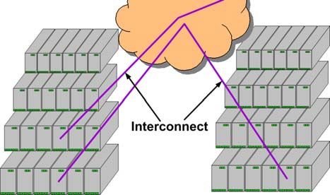
MCM: Multi chip module, a specialized electronic package where multiple integrated circuits (ICs),
semiconductor dies or other discrete components are packaged onto a unifying substrate, facilitating their
use as a single component (as though a larger IC).

Mid-board optics: an optical transceiver that is mounted on a PCBA away from the PCBA edge, close to a
switch ASIC to reduce the amount of PCBA trace loss between an ASIC and the optical transceiver. This is
in contrast to the common practice today of locating optical transceivers at the PCBA edge.

MMF: Multimode fiber, a type of optical fiber mostly used for communication over short distances, such as
within a building or on a campus

MPO: Multi Pin Push On, an optical ferrule containing multiple fibers. MTP is trademarked version of MPO.

MUX/DEMUX: Multiplex / demultiplex, a multiplexer (or mux) is a device that selects one of several analog
or digital input signals and forwards the selected input into a single line, Conversely, a demultiplexer (or
demux) is a device taking a single input signal and selecting one of many data-output-lines, which is
connected to the single input.

NRZ: Non return to zero, a binary code in which 1s are represented by one significant condition (usually a
positive voltage) and 0s are represented by some other significant condition (usually a negative voltage),
with no other neutral or rest condition.

O-to-E and E-to-O: Optical to electrical interface and Electrical to optical interface, a component that
converts an optical signal to an electrical signal or vise versa.

OFDM: Orthogonal frequency duplex modulation, a method of encoding digital data on multiple sub carrier
frequencies

PAM: Pulse amplitude modulation, a form of signal modulation where the message information is encoded
in the amplitude of a series of signal pulses. For optical links it refers to intensity modulation.

PAM-4: Pulse amplitude modulation-4 is a two-bit modulation that will take two bits at a time and will map
the signal amplitude to one of four possible levels.

PCBA: Printed circuit board (PCB) assembly, an assembly of electrical components built on a rigid glass-
reinforced epoxy based board.

QAM: Quadrature amplitude modulation (QAM) is both an analog and a digital modulation scheme. It
conveys two analog message signals, or two digital bit streams, by changing (modulating) the amplitudes of
two carrier waves, using the amplitude-shift keying (ASK) digital modulation scheme or amplitude
modulation (AM) analog modulation scheme. The two carrier waves, usually sinusoids, are out of phase
with each other by 90° and are thus called quadrature carriers or quadrature components- hence the name
of the scheme.

RS: Reed Solomon FEC coding, this is a type of block code. Block codes work on fixed-size blocks
(packets) of bits or symbols of predetermined size. It can detect and correct multiple random and burst
errors.

SMF: Single mode fiber, an optical fiber designed to carry only a single ray of light (mode), which allows it to
be used for communication over longer distances than multi mode fiber.
                                                                                                               12
Tb/s: Terabits per second. The stated throughput or data rate of a port or piece of equipment. Tb/s is 1x10
bits per second

VCSEL: Vertical cavity surface emitting laser is a type of semiconductor laser diode with laser beam
emission perpendicular from the top surface.

WDM: Wave division multiplexing, a technology which multiplexes a number of optical carrier signals onto a
single optical fiber by using different wavelengths (i.e. colors) of laser light.

† Some definitions include content from www.wikipedia.com

    www.oiforum.com                                                                                            6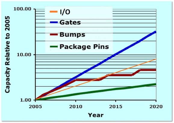
1 Executive Summary

   In the past the OIF has supported the communications industry by generating
   implementation agreements that have been shared openly with other industry standards
   bodies. These implementation agreements have defined the parameters and required
   performance levels necessary to support the development of cost and power effective
   broad industry ecosystems. As the OIF anticipates the next generation of higher data rate
   systems, it is becoming apparent that new technological solutions will be required at many
   levels of the future communication systems. The objective of this framework document is
   to identify and define the hardware application spaces that could possibly benefit from
   future OIF Implementation Agreements across the multiple levels of hardware. Identifying
   and defining these application spaces will allow the OIF and others in the industry to have
   a common language, or understanding, as decisions are made to initiate new development
   projects.

   The technical challenges of next generation data rate systems are discussed as well as
   test interoperability issues that will need to be addressed for the various interconnection
   applications. Although some technical options are mentioned, it is not the scope of this
   document to define specific technical solutions for these applications or the priority with
   which the application spaces should be addressed.

   As in the past, it is critical that the industry maintain interoperable interfaces for application
   spaces to enable cost effective component, subsystem, and system development and
   deployment. This will ensure interoperable fiber, connectors, electrical interfaces, etc.
   Identification of the critical application interconnections is the first step to meeting this
   requirement. The goal of this document is to build consensus across the industry on the
   applications spaces and motivate the initiation of collaborative discussions that are
   required to generate a broadly agreed set of project developments and objectives.

 www.oiforum.com                                                                                    7
2 Introduction
2.1 Purpose
The OIF Next Generation Interconnect Framework identifies application spaces for next
generation systems and identifies areas for future work by the OIF and other standards
bodies. The scope of this document explores Next Generation (NG) Interconnects that are
limited to data center or intra-office applications which are generally less than 2km from
both an electrical and optical perspective. Virtual Platforms in the cloud is an example of
just one of the applications that will take advantage of NG Interconnect technology to
achieve higher data bandwidths in a smaller footprint with better energy efficiency.
Figure 1 Interconnect Application Spaces
As shown in Figure 1, interconnection interfaces in a typical system are needed for chip-to-
chip within a module, chip to chip within a PCBA (printed circuit board assembly), between
two PCBAs over a backplane/midplane, or between two chassis’. These interfaces may be
unidirectional or bi-directional, optical or electrical, and may support a range of data rates.
For each application space, the IAs that follow from this framework should identify
requirements to support interoperability across the various application spaces for optical
and electrical links. They may include, but not be limited to:
Cost Considerations
Link Performance
Power Consumption
www.oiforum.com 8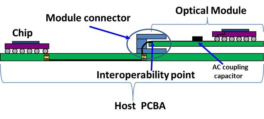
Loss budgets, signal levels, and timing
Number of lanes, channel configuration and general characteristics
Link Latency
Connector requirements and/or configurations
Optical wavelengths/ frequencies
MMF/SMF & waveguides
Reliability Considerations
Size Considerations
Operating Temperature Considerations
The Framework Document may recommend a number of follow-on subprojects to address
interoperability for specific application spaces.
2.2 Motivation
Next generation systems are being driven by the need to handle the increasing volume of
data traffic. At the same time, the next generation systems are constrained by limits on
power consumption, by limits on the size of a system, and by the need to provide a cost
effective solution.
These needs drive next generation systems to ever increasing communication port
densities. The increased density leads to smaller surface areas available to dissipate the
heat generated and therefore requires decreased power consumption for a port.
As an example, let’s look at a current “state of the art” deployed high-end telecom system
which comprises a small chassis with 20 blades capable of processing 500Gb/s of full-
duplex data per blade using optical interconnects. To scale a system beyond a single
chassis of equipment requires an uplink trunk capacity of 10Tb/s. Currently, to
accommodate a 10Tb/s data pipe using 10Gb/s channels would require 1000 ingress and
1000 egress data channels, whereby a channel is representative of a single waveguide
such as an optical fiber or wavelength.
Indeed, using “thousands” of optical fibers for connecting a single chassis to a hub would
be impractical from a physical constraints perspective. On the other hand, if 25Gb/s
channels are used, then a total of 800 optical fibers are required which still seems
undesirable. Alternatively, a more practical number of optical fibers could be reached by
using a combination of: higher baud rates, increased bits per symbol, and optical
wavelength or polarization multiplexing schemes.
The industry currently has electrical interfaces for 10Gb/s (OIF’s CEI-11G), 25Gb/s &
28Gb/s (OIF’s CEI-25/28G) at its disposal and work is starting on 56Gb/s (OIF’s CEI-56G)
to meet higher date rate needs. However, copper interconnects are severely bandwidth
limited and it is increasingly difficult to achieve the same link distances using higher
signaling rates.
A reasonable assumption is that 40Tb/s data interconnects will eventually become reality
for interconnecting high-end system components to an optical network fabric “hub”. Shown
below in Table 1 are some of the possible strategies for the design of a 40Tb/s optical data
interconnect. Multiplying the design parameters in columns 2 through 4 equates to the
required “Data Rate per Fiber” and “Number of Optical Fibers” which are noted in columns
5 & 6 respectively.
A bundle of a hundred or less optical fibers could be considered an acceptable sized
optical conduit which satisfies both a small bend radius to facilitate cabling, and dense end
terminations with 6x12MTP/MPO-like connectors. For a 40Tb/s optical data interconnect, a
www.oiforum.com 9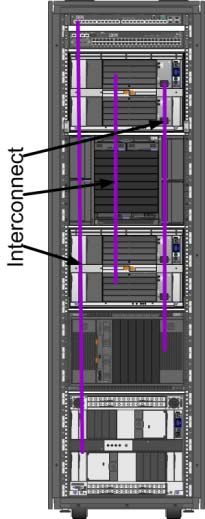
data rate of 400Gbps per fiber or better is desirable to condense connectivity into 2 cables
   made of 100 optical fibers using two connectors each.
                       Table 1 Forward Looking Optical 40Tbps Scenarios

           Effective       Bits     Symbol     Wavel.     Data Rate        No. of
             Speed         Per       Rate       per       per Fiber        Links
           Scenarios     Symbol     (GSps)     Fiber       (Gbps)         (Fibers)
            1x10G           1          10          1           10          8000
            1x25G           1          25          1           25          3200
            1x40G           1          40          1           40          2000
            1x50G           1          50          1           50          1600
            4x25G           1          25          4           100          800
            2x50G           2          50          1           100          800
            8x25G           2          25          4           200          400
            16x25G          2          25          8           400          200
            10x40G          1          40         10           400          200
            8x50G           2          50          4           400          200
            20x40G          2          40         10           800          100
            16x50G          1          50         16           800          100
            40x40G          4          40         10          1600          50
            32x50G          4          50          8          1600          50

   Multicore fiber & Dual-polarization schemes are future potential solutions which require
   further maturity to target economical interconnects. As an example, multi-core fiber could
   increase the number of links per fiber, but is incompatible with current high density
   connectors.

   Improvements in IC integration, which has been relentlessly driven by Moore’s Law over
   past decades, have come to the rescue enabling higher densities of logic gates at
   escalating higher clock rates to be used in IC designs. These trends have allowed the
   industry to deploy increasingly more complex communication systems at each generation
   to meet the infrastructure needs.

   However, as one digs deeper, the future appears to be challenging. Many different
   technologies need to converge to improve the throughput. These complex ICs have
   increasing gate counts, but the power dissipation per gate and I/O speed are no longer
   scaled at the same rate as the gate count. In addition, the numbers of electrical
   connections (bumps and package pins) are also not scaling at the same rate - leading to a
   power, capacity and port count gap for the next generation interconnect interfaces.

www.oiforum.com                                                                                 10
Figure 2 Scaling Gates/Bumps/Pins (Ref. Xilinx, I/O Line Added)
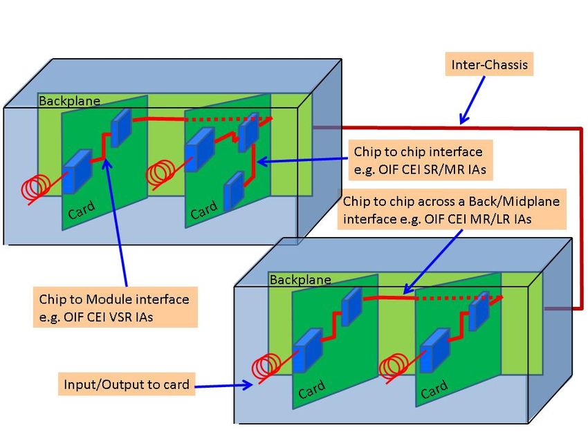
The predominant Next Generation Interconnect challenges to overcome are presented
below in a solution space diagram, and are discussed in greater detail in subsequent sub-
sections.
Figure 3 Next Generation Interconnect Challenges
www.oiforum.com 112.2.1 Challenges of Power Dissipation
If the architecture of a “virtual” host chip results in the chip package exceeding the
maximum power dissipation, the chip’s functions must be broken down into multiple
devices. Creating a large “virtual” chip that comprises multiple smaller chips that are
interconnected by a network fabric will require each chip slice to accommodate extra
peripheral ports for interconnectivity. In effect, the chipset as a whole will probably have
increased power dissipation due to the additional power required to communicate between
multiple devices in order to retain context and the transmission of signals between chips.
In addition, system power requirements have challenges, as in the case of ASIC’s targeting
lower voltage power sources as is the trend with smaller technology nodes. The net effect
of higher integration of low voltage semiconductors is a significant increase in total device
power, which in effect requires extremely high current source power supplies which must
be controlled within several mV tolerances, which in turn requires additional power pins per
device to accommodate the high electrical currents.
Furthermore, system cooling can escalate beyond physical limits as well, and therefore
every power saving initiative is more than welcome.
Since the I/O power is related to the distance that the electrical signals travel for a given
channel’s properties, reducing the distance that the electrical signal must be driven can
reduce power dissipation. In a real system implementation, it may not be practical to
reduce the physical distance, so the reduced electrical reach can be achieved with re-
timers or repeater devices, to the detriment of cost and power, or with the use of mid-board
optics.
In some cases, it may make sense to integrate the optics into the chip package, thereby
eliminating the necessity to drive electrical signals outside the device, which would enable
a consistent power budget over a broad range of channel lengths. However in this case,
the optics would be required to work over a much broader temperature range.
2.2.2 Challenges of I/O Densities on Chips and Connectors
The maximum number of useful I/Os for high speed serial links per device is not only
limited by the available package technology itself, but also by the ability to route the device
on the PCBA.
In order to maintain signal integrity for a high speed serial link design, it is required to be
able to route a differential pair between two package balls when escaping from the inner
ball rows of a ball grid array (BGA), and it therefore may become more costly to use
packages with a ball pitch below 1.0 mm.
In addition, for every ball row from the edge of the package on which differential pairs have
been placed, a separate circuit package layer has to be used. Differential pairs in the outer
4 rows of the BGA requires 4 signal layers on the PCBA, while the 6 outer rows would
require 6 layers, and thus the PCB layer stack grows with every inner BGA row to be
routed.
It may also be beneficial and indeed necessary to increase the baud rate of a channel to
improve the data rate and drive down the number of I/Os required. The data rate can be
increased by using higher signaling rates and/or advanced modulation formats such as
PAM, DMT, or OFDM.
www.oiforum.com 122.2.3 Challenges of Channel Characteristics
Link applications are characterized by the supported loss budget. Loss is determined by
link length, number of connectors and passive loss elements including splitters. Increases
in signaling rate cause lower SNR. Further, advanced modulation schemes are considered
for improving the maximum data rate of a bandwidth limited electrical channel. These
require a higher SNR for equivalent BER. Forward error correction (FEC) is one technique
which increases the SNR and therefore the supported loss budget at the expense of higher
power dissipation, complexity, and latency. Bandwidth limitations and increases in
signaling rate result in impairments such as increased jitter that may be compensated by
using equalization techniques that will impact power consumption and complexity. If a
green field approach is possible, advanced materials for the channel (PCB and connector)
can result in an increased electrical data rate.
Furthermore, improved optical modulation methods may extend the use of MMF
interconnect deployments as signaling speeds increase. For example, premium grade
OM4 MMF fiber has an EMB – Effective Modal Bandwidth of 4700 MHz-km which can
support reaches of 400 meters at 10 Gb/s using NRZ encoding. Compressing more
bits/symbol as in the case of advanced modulation may result in ~30Gb/s transmissions
over OM4 MM fiber with a reach of 200 meters at the expense of additional power
consumption.
WDM or denser waveguide e.g. multiple fibers or multicore fibers (MCF) are alternate
approaches to increasing data rate, but also at the expense of introducing new
complexities in IC chip packaging such as: optical waveguide transpositions, optical
MUX/DEMUX or fine pitch multi-core fiber attachment based on SM waveguides.
At the end, there is always a trade-off between power, material cost, and circuit complexity.
An on-going challenge to be considered is the connector loss associated with structured
cabling which is necessary for operational management. An optical link is characterized by
both, reach and loss budget, for example 2km and 4dB or 10km and 6dB.
2.2.4 Challenges of Electrical Link Reach
In a communication system usually the front plate area is occupied by pluggable modules
for inter-system communications, while the intra-system traffic between the PCBAs is
connected over the backplane/midplane. To support reasonable system dimensions,
system backplane/midplane connections typically need to bridge distances of up to 70–100
cm (28–40 in). At electrical serial speeds of 25 Gb/s, reaches at such distances already
require the use of advanced low loss circuit package materials and connectors to meet the
loss budget. Furthermore, increasing the electrical link speed will increase the losses at
Nyquist rates and therefore will significantly reduce the possible link reach.
Advanced modulation schemes can help to maintain the loss budget by reducing the
Nyquist frequency, but they come with a power penalty as a result of the increased signal
to noise ratio (SNR) requirements. One solution to overcome the SNR degradation is the
use of FEC.
When considering the link reach, the conventional focus is the typical PCBA copper trace
and connector constructions but potentially the electrical interconnect traces could be
www.oiforum.com 13replaced by better performing micro-coax and/or flex circuits. Another advantage of flex
and micro-coax is that the PCBA could then be built from low cost material. The use of
micro-coax and flex does have its own share of challenges especially in the attachment
process and rework operation.
Another opportunity to affect link reach is the substrate materials used in the chip
packaging. The package substrate materials especially for the next generation data rate
applications will require improvement over current package substrates which have losses
comparable to standard FR4.
The introduction of repeater devices into the data path increases reach at the expense of
added complexity.
Finally, a migration to optical interconnections for backplane/midplane applications may
provide a roadmap which can accommodate increasing data rates, while simultaneously
maintaining the ability to bridge a reasonable distance for intra-system connections.
For shorter reach applications on a single PCBA, as in a chip-to-module, the same problem
of insufficient link reach will probably show up just at twice or four times the speed.
Nevertheless, similar solutions will be required to continue to increase future generation
system densities.
2.3 Summary
As time proceeds, ICs will become faster and denser. To cope with the issue of
interconnect capacity and density of future systems, photonic interconnects will become an
even more important connection technology.
The implementation of NG (Next Generation) Interconnects technology poses several
challenges especially in relation to: bounded power dissipation, limited I/O density,
maximum channel data rate, and optimal electric/optical reach. Highlighted were the side-
effects of some solutions, which are a result of the complex inter-dependencies of: higher
integration, complex modulation schemes, chip break-out and routing, signal conditioning,
thermal & power issues, package footprint, etc.
In conclusion, further study is required to decide on a solution for each of the challenges
identified, in order to achieve a cost effective NG Interconnect solution that satisfies the
power density (watt/meter2) requirement.
The Next Generation Interconnect Framework explores the interconnect needs for next
generation systems and identifies applications for possible work at the OIF or other
standards bodies to address the industry’s next generation needs.
The purpose of this document is to foster communications between optical interworking
technology users & providers, which comprises an ecosystem of: system vendors, optical
OEM’s, and silicon component fabricators. Also, this document is to serve as a “Statement
of Understanding” between optical interworking technology users and providers, for
achieving coordinated solutions for NG Interconnects.
www.oiforum.com 143 Interconnect Applications
The NG interconnect application spaces mentioned in section 2 can be broken down into
the following applications.
Figure 4 Interconnect Application Spaces
3.1 Die to Die Interconnect Within A Package
Figure 5 Die to Die within an MCM Interconnect Application Space
It may be necessary to use multiple dies within a multi-chip module (MCM) to achieve the
industry’s objectives. These co-packaged solutions can communicate with less power
since the substrate provides a high quality communication channel.
www.oiforum.com 15The communication channel would typically be less than 15mm. This short electrical link
may allow for a much simpler interface and require less power than an existing standard
electrical interface. For example, equalization is unlikely to be needed and it may be
possible to assume such short links are synchronous (single reference clock going to all
chips), removing the need for a frequency tracking CDR.
Future dies may also have direct optical input/output, such that the die to die interconnect
would be optical.
3.2 Die to optical engine within a package
Figure 6 Die to Optical Engine MCM Interconnect Application Space
It may be necessary to use a die and an optical engine within a multi-chip module (MCM)
to achieve the industry’s objectives. These co-packaged solutions can communicate with
low power since the substrate provides a high quality communication channel.
The communication channel would typically be less than 15mm. This short electrical link
may allow for a much simpler interface and require less power than an existing standard
electrical interface.
If the optical link uses advanced modulation formats such as PAM or DMT schemes it may
also be of benefit for the electrical links to support the same modulation scheme. Then it
would be possible that the processing of the modulation scheme would be in the chip (i.e.
the optical engine just needs to convert signals linearly across the O-to-E & E-to-O
interfaces).
3.3 Chip to Nearby Optical Engine
Figure 7 Chip to nearby OE Interconnect Application Space
It may be useful to place an optical interface very close to the host chip (rather than placing
the optical device within a host MCM due to heat restrictions of the optical components). In
this case, a short electrical link of less than 50mm is anticipated. Although this type of link
will require more power than a link within a multi-chip module, the short reach of this
www.oiforum.com 16channel would still imply power could be saved. Again advanced modulation formats may
be appropriate for such links if the optical side uses these formats.
3.4 Chip to Module
Figure 8 Chip to Module Interconnect Application Space
It is common in modern communication systems to support pluggable modules at the front
faceplate of the equipment. This facilitates low cost initial deployment of the equipment if
some ports are left unpopulated. A pay as you grow policy is then used until the entire
faceplate is populated with pluggable modules. The electrical link used to connect these
pluggable modules can extend to beyond 30cm. At higher data rates this challenges the
ability of the host chip to drive these long trace lengths within the power constraints of large
switch chips. Placing retiming devices inside the pluggable module provides support for
longer host traces but the inclusion of complex equalization features can overburden the
limited power budgets of the pluggable module. Advanced modulation formats (such as
PAM or DMT schemes), Forward Error Correction (FEC) and equalization features are all
possible solutions for the chip to module interconnect.
3.5 Chip to Chip within PCBA
Figure 9 Chip to Chip Within PCBA Interconnect Application Space
An interconnection interface may be needed between two chips on the same PCBA or on a
daughter card or shorter mid-plane. By definition, this interface is relatively short ranging
from 1cm to perhaps 40cm. This interface could include a single connector. Further this
category is typically split into 2 groups, a short reach (SR) from 1cm to 20cm and medium
reach (MR) from 1cm to 40cm.
Most SR environments can save power if one can assume that both chips use the same
power sources and the same reference clock, so that the signal noise sources are reduced
in comparison to systems where the devices at each end of a channel are fully
independent.
This interface would conventionally be electrical. It would, however, also be possible to
use a combination of electrical and optical interfaces or even optical waveguides within the
PCBA.
www.oiforum.com 173.6 PCBA to PCBA across a Backplane/Midplane
Figure 10 PCBA to PCBA Across a Backplane/Midplane Interconnect Application Space
This interface communicates between two cards across a backplane/midplane within a
chassis and is less than 1m with up to 3 connectors.
This interface would conventionally be electrical. Due to the longer length channel, these
interfaces would resemble the OIF’s CEI type solutions. It would however also be possible
to use a combination of electrical and optical interfaces or even optical waveguides within
the PCBA.
In addition, it may be appropriate to use advanced modulation formats such as PAM or
DMT schemes in the link allowing for increased throughput density at the same baud rate.
FEC may be a requirement to meet the BER – however the choice of the FEC must be
considered carefully to address both latency and power concerns. Possible FEC
implementations are RS or BCH.
www.oiforum.com 183.7 Chassis to Chassis within a Rack
Figure 11 Chassis to Chassis within the Same Rack Interconnect Application Space
This interface ranges up to 3m and could be either optical or electrical. Wider interfaces
(i.e. optical multi fiber cable or parallel pair copper cables) could be analyzed for this
application.
It may be appropriate to use advanced modulation formats such as PAM or DMT schemes
in the link allowing for increased throughput density at the same baud rate.
FEC may be a requirement to meet the BER – however the choice of the FEC must be
considered carefully to address both latency and power concerns. Possible FEC
implementations are RS or BCH.
3.8 Rack to Rack side‐by‐side
Figure 12 Rack to Rack side-by-side Interconnect Application Space
This interface ranges from 3 to 10m and could be either optical or electrical. Wider
interfaces (i.e. optical multi fiber cable or parallel pair copper cables) could be analyzed for
this application.
It may be appropriate to use advanced modulation formats such as PAM or DMT schemes
in the link allowing for increased throughput density at the same baud rate.
www.oiforum.com 19FEC may be a requirement to meet the BER – however the choice of the FEC must be
considered carefully to address both latency and power concerns. Possible FEC
implementations are RS or BCH.
3.9 Rack to Rack in the same row
Figure 13 Rack to Rack in the Same Row Interconnect Application Space
This interface ranges from 15 to 50m and is either MMF or SMF optical. Wider interfaces
(ie multi fiber cable) could be analyzed for this application. It may be advantageous to use
FEC to relax the optical link budget – however the choice of the FEC must be considered
carefully to address both latency and power concerns. Possible FEC implementations are
RS or BCH.
www.oiforum.com 203.10 Rack to Rack in the same building
Figure 14 Rack to Rack in the Same Building Interconnect Application Space
This interface ranges from 100 to 300m and is either MMF or SMF optical. Wider interfaces
(ie multi fiber cable) could be analyzed for this application. It may be advantageous to use
FEC to relax the optical link budget – however the choice of the FEC must be considered
carefully to address both latency and power concerns. Possible FEC implementations are
RS or BCH.
www.oiforum.com 213.11 Rack to Rack in the same data warehouse
Figure 15 Rack to Rack in the Same Data Warehouse Interconnect Application Space
This interface ranges from 300m to 1km and is SMF optical. Parallel fiber interfaces could
be investigated, but the cost of the fiber needs to be considered. If parallel fiber interfaces
are not used, more efficient signaling schemes and/or WDM techniques optimized for short
reach will be required. Some of the more efficient signaling schemes suitable for optical
transmission are lower order PAM (such as PAM-4) or DMT/QAM/CAP. As the baud rate
increases and/or higher order constellation is used, FEC may be required to close the link
budget. The choice of the FEC must be considered carefully to address both latency and
power concerns. Possible FEC implementations are RS, BCH or BCH cross-product for
higher gain if needed.
www.oiforum.com 223.12 Rack to Rack in the same campus
Figure 16 Rack to Rack in the Same Campus Interconnect Application Space
This interface ranges from 1 to 2km and is SMF optical. More efficient signaling schemes
and/or WDM techniques optimized for short reach are required. Some of the more efficient
signaling schemes suitable for optical transmission are lower order PAM (such as PAM-4)
or DMT/QAM/CAP. As the baud rate increases and/or higher order constellation is used,
FEC may be required to close the link budget. The choice of the FEC must be considered
carefully to address both latency and power concerns. Possible FEC implementations are
RS, BCH or BCH cross-product for higher gain if needed.
3.13 Longer than 2km links
Although there are links that are longer than 2km, these are considered outside the scope
of this document.
3.14 Interconnect Application Summary
Table 2 Intra-Interconnect Applications
Intra Interconnect Application Distance Up To Types of interfaces
Die to Die in a Package ~ 15mm Electrical or Optical
Die to Optical Engine in a Package ~ 15mm Electrical
Chip to nearby optical Engine ~ 50mm Electrical
Chip to pluggable module ~ 100-150mm Electrical
Chip to chip within PCBA ~ 40cm Electrical or Optical
PCBA to PCBA across a ~ 1m Electrical or Optical
backplane/midplane
www.oiforum.com 23Table 3 Inter-Interconnect Applications
Inter Interconnect Application Distance Up To Types of interfaces
Chassis to Chassis within a rack ~ 3m Electrical or Optical
Rack to Rack side-by-side ~ 10m Electrical or Optical
Rack to Rack within a row ~ 50m Optical (MMF/SMF)
Rack to Rack within a building ~ 100-300m Optical (MMF/SMF)
Rack to Rack within a data
~ 1,000m Optical (SMF)
warehouse
Rack to Rack within a campus ~ 2km Optical (SMF)
www.oiforum.com 244 Points of Interoperability
The Optical Internetworking Forum (OIF) promotes the development and deployment of
interoperable networking solutions and services through the creation of Implementation
Agreements (IAs) for optical networking products. It is therefore important for any next
generation interconnects to consider the interoperability points to be defined in the
agreement. The IA must also develop realistic measurement techniques for the defined
interoperability test points.
A next generation interconnect may be either electrical or optical. The possible
interoperability points are shown in Figure 17 below.
Figure 17 Interconnect Application Space Showing Points of Interoperability
4.1 Electrical Channel points of interoperability
4.1.1 Die to Die, Chip to Chip, Back/Midplane, Chip to Optical engine
interconnects
Electrical interconnects between die in a multichip module, between chips on a PCBA,
between chips across a backplane/midplane or between a chip and an optical engine have
similar points of interoperability as shown in figure 18. Each of these electrical
www.oiforum.com 25interconnects begins at a die/chip that is soldered on a MCM/PCBA and ends at another
die/chip that is soldered onto a MCM/PCBA. The electrical channel varies in length,
number of connectors and attenuation but the definition of the interoperability points can be
the same.
Figure 18 Chip to Chip Interop Points
4.1.1.1 Challenges of defining chip to chip interoperability points
The chip to chip interoperability points are best defined at the ball of the IC or packaged
device. This allows chip makers to design directly to the specification and avoids the
confusion of defining a load channel, which may not represent the real life system
interconnect. The challenge with this method is the verification of compliance at a point that
is not measureable in a real system.
4.1.1.2 Possible solutions for the definition of interoperability points for chip to
chip interconnects
Compliance to the specification could be done by de-embedding the system electrical
interconnect from the nearest separable interface to the chip. This would provide a
common point to evaluate chip specification but depends on a robust and repeatable de-
embedding algorithm. In practice this has been difficult to achieve. An alternative method
would be to measure the signal at the end of a defined ‘compliance’ channel. The
compliance channel is defined to be a short distance from the ball using a low loss test
path and high bandwidth connectors. (See figure 19) This solution requires a well defined
compliance channel using low loss PCB materials and high frequency connectors.
Figure 19 Backplane/Midplane Interoperability Point
www.oiforum.com 264.1.2 Chip to module interoperability points
The chip to module interconnect contains a separable connector at the faceplate of the
host equipment. This provides a natural point to test for interoperability. Figure 20 shows a
number of different connectors on the faceplate of a switch. The interoperability definition is
between a host connector/socket and a pluggable module.
Figure 20 Pluggable Modules on Front Faceplate
The interoperability point for a chip to module interconnect as shown in figure 21 is the
pluggable module connector.
Figure 21 Chip to Module Interoperability Point
4.1.2.1 Chip to module interoperability point challenges
The chip to module interoperability points are best defined at the host connector interface.
This allows both the host and module designers to verify their designs directly against the
specification. The challenge is to specify a signal in the middle of a connector. A reference
test board with the mating connector is required to provide measurement points that can be
used by test equipment.
4.1.2.2 Chip to module interoperability definition possibilities
The chip to module interoperability points can be measured at the end of a host or module
compliance board. The characteristics of the host compliance board (HCB) are intended to
emulate the trace loss of the optical module. An example of this can be found in the OIF-
CEI-28G-VSR specification. The challenge that needs to be solved is to create a
compliance board with very low loss and good signal integrity. In practice these have been
www.oiforum.com 27difficult to achieve and without additional invention it may not be possible with higher signaling rates. The module compliance board (MCB) must have low loss to minimize the effects on the measurement but the shorter trace length makes it less of a challenge. An alternative method is to de-embed the compliance board from the measurement. This is difficult to do because of lack of precision calibration capabilities at the measurement point. The impedance discontinuities caused by the connector interface have also proven to be difficult to de-embed. www.oiforum.com 28
5 Opportunities for Future Work

      5.1    Introduction
   Section 3 identifies the many applications where next generation systems might benefit
   from an identified interconnect definition or “Implementation Agreement (IA)”. All of these
   “interconnections” are possible areas for new projects within the OIF or other Standards
   bodies. The following paragraphs identify a few additional specific areas that might be
   investigated for future OIF activities.

      5.2    Electrical Interconnect
   The primary focus of the Chip to Chip and PCBA to PCBA sections 3.5 and 3.6 of this
   framework document are the classic PCBA and connector constructions. Possible topics
   for future investigation include advanced system architectures, advanced modulations, and
   lower loss interconnection systems.

   Another area that is worthy of future study is packaging trends toward 2.5D and 3D stacks
   with silicon interposer technology or other emerging packaging technologies which may
   solve some of the electrical characteristics that limit higher bandwidths in the applications
   described in sections 3.1 and 3.2.

 5.2.1 Electrical Connectors
   Improved high density connectors with smaller pitches may be necessary to enable high
   speed applications with efficient signaling and/or higher baud rate. Some of these issues
   have already been seen such as in the case of the CFP2/CFP4 connector pitch limit.
   Particular attention needs to be given to the electrical connector characteristics through S-
   parameter optimization. Additionally, with upcoming optoelectronic devices on board to
   solve the higher signaling density, hybrid optical/electrical connectors may be needed.

   Onboard optical devices, such as mentioned in section 3.3, take advantage of ball grid
   array packaging and may offer much higher port density compared to pluggable modules.
   Some of the first generation optical devices may not withstand reflow process and likely will
   require a board socket. Development of high performance sockets for optical components
   that are capable of 56 GBd is highly desirable.

 5.2.2 Electrical Links
   OIF is now actively developing next generation electrical interfaces including: CEI-56G-
   USR (Ultra Short Reach), CEI-56G-CPR (Close Proximity Reach), and CEI-56-VSR (Very
   Short Reach) to address the applications described in sections 3.1, 3.2, 3.3 and 3.4.
   Currently these interfaces are assumed to be either NRZ or PAM-4. Two areas that do not
   yet have OIF projects are development of a chip to chip in a PCBA (section 3.5) and
   backplane/midplane channel (section 3.6) for 56 Gb/s.

   An additional area to investigate is an electrical channel for short cable reaches such as 3
   meters within a rack “chassis to chassis” interconnect as described in paragraph 3.7.

www.oiforum.com                                                                                29
5.3 Optical Interconnect
There is currently a significant amount of research on optical circuit and packet switching.
A major obstacle in optical switching is lack of buffers and therefore the network must be
architected based on this fact. Optics mounted on the PCB and optics co-packaged with
the host chip such as silicon photonics each can increase the system bandwidth by about
an order of magnitude over pluggable modules. At some point the bandwidth limit either in
the EO/OE or on the system host chip is reached, where the only option to further increase
the bandwidth is with optical switching.
Free space optics and on chip optical communications are not currently considered in this
framework document but could be the subject of future work.
5.3.1 Optical Connectors
Today many types of connectors are developed and three general categories are of
interest. First are connectors used for bulkhead or module interfaces; these connectors
tend to be large and robust so they can support pulling forces in excess of 20 Newtons.
The second type of connectors designed for high density and small footprint is used for
board to board and chip to chip. A third type of connectors requires the capability for high
density blind mating with reduced sensitivity to contaminants for hybrid and optical
backplane/midplane applications. Each of these three connector categories has its own
challenges.
The need in these increasingly critical high density areas are for micro optical connectors
with optimized optical characteristics to handle the requirements of new modulation
schemes in addition to supporting different types of optical media such as fiber, and
waveguides. Some promising work is beginning to demonstrate these capabilities and
performance with more improvements expected. Hybrid optical and electrical connectors
may also be required for next generation’s higher levels of integration.
5.3.2 Optical Links
The use of parallel optics, advanced modulation and WDM are all likely choices to increase
the bit rate and density as mentioned earlier. At this point in time, orthogonal modulation in
the optical domain and polarization modulation are not considered due to cost and
complexity, but potentially with the emergence of more advanced silicon photonics some of
these schemes could become more feasible for shorter reach applications.
In addition to using fibers (single or multi fiber) for the interconnect between two optical
devices, the increase of density, bandwidth and more integration is trending toward new
technology that is summarized below:
Optical waveguides integrated into a package substrate or standard PCB that may
be used for short reach links. These might be adequate for solving density and
future integration. For adoption of these integrated waveguides, there are still
several issues that need to be solved such as optical via losses, transitions from
vertical to horizontal launch, etc. As these technical challenges are addressed, the
OIF could start projects to develop documented methods of interconnecting these
waveguides.
Multi-core fiber (MCF) for single mode or multimode is a promising technology but
due to a current lack of cost effective precision connector methodology, these links
are not considered in this framework document. MCF could be used to increase
port densities by a significant factor. MCF could provide an alternative for
www.oiforum.com 30You can also read