A Time Amplifier Assisted Frequency-to-Digital Converter Based Digital Fractional-N PLL - Integrated Signal Processing Group
←
→
Page content transcription
If your browser does not render page correctly, please read the page content below
IEEE JOURNAL OF SOLID-STATE CIRCUITS, VOL. 56, NO. 9, SEPTEMBER 2021                                                                                       2711

      A Time Amplifier Assisted Frequency-to-Digital
        Converter Based Digital Fractional-N PLL
              Eslam Helal , Enrique Alvarez-Fontecilla , Amr I. Eissa , and Ian Galton , Fellow, IEEE

    Abstract— This article presents a wide input-range delay
chain based time amplifier (TA) and its application to a 6.5-GHz
digital fractional-N phase-locked loop (PLL). The TA includes a
delay-averaging linearity enhancement technique and the PLL
is based on an improved dual-mode ring oscillator (DMRO)
delta-sigma () frequency-to-digital converter (FDC). The TA
mitigates contributions to the PLL’s phase noise from DMRO
flicker noise, which would otherwise degrade the PLL’s in-band
phase noise, and from  FDC quantization error, which would
otherwise degrade the PLL’s phase noise at high bandwidth
settings. This paper also presents a delay-free asynchronous
DMRO phase sampling scheme, and the first experimental
demonstration of a recently-proposed  FDC digital gain
calibration technique. The TA-assisted PLL achieves a random
jitter of 145 fsrms , a total jitter that ranges from 151 to 270 fsrms
as a result of fractional spurs, and a worst-case fractional spur
of −49 dBc without requiring nonlinearity calibration.
   Index Terms— Averaging resistors, delta-sigma () modula-
tion, digital phase-locked loop (PLL), dual-mode ring oscillator
(DMRO), frequency synthesizer, frequency-to-digital converter
(FDC), gain calibration, jitter, phase sampling, time
amplifier (TA).

                           I. I NTRODUCTION

M      ANY types of phase-locked loops (PLLs) use a phase-
       frequency detector (PFD) with subsequent circuitry to
measure the time differences between corresponding edges of
                                                                                  Fig. 1. (a) High-level block diagram of the PLL, (b) simplified block diagram
                                                                                  of the TA-assisted DMRO  FDC, and (c) details of the RPC with gain
                                                                                  calibration.
the reference signal and a divided-down version of the PLL
output signal. In such PLLs, using a time amplifier (TA) to                       TA presented in [6] avoids most of these issues, but its rela-
amplify the edge time differences prior to the PFD and sub-                       tively complicated implementation limits its noise performance
sequently dividing the measured time differences by the gain                      which reduces its suitability for high-performance PLLs.
of the TA attenuates the noise introduced by the measurement                         A low-noise inverter based delay chain TA with an analog
process without otherwise changing the loop dynamics.                             delay-averaging nonlinearity mitigation technique is presented
   Several TAs have been proposed over the last two                               in this paper. The gain of the TA is nearly constant across a
decades [1]–[6], yet most suffer from significant drawbacks                       wide input range and is relatively insensitive to process, volt-
such as narrow input range [1]–[4], gain and input range                          age, and temperature (PVT) variations, as it depends on a ratio
dependency on technology parameters [1]–[4], high nonlinear-                      of inverter delays. The TA’s principle of operation is similar
ity [1]–[5], a tradeoff between gain and input range [1]–[3],                     to that of the TA presented in [6], but its implementation is
and a tradeoff between linear input range and noise [4]. The                      simpler and it achieves better noise performance.
                                                                                     The proposed TA is demonstrated in the context of a
  Manuscript received October 17, 2020; revised December 8, 2020 and              6.5 GHz digital fractional-N PLL based on a dual-mode
December 22, 2020; accepted December 23, 2020. Date of publication Febru-
ary 2, 2021; date of current version August 26, 2021. This article was approved   ring oscillator (DMRO) delta-sigma () frequency-to-digital
by Associate Editor Pietro Andreani. This work was supported by the               converter (FDC) [7]–[9]. As demonstrated in [7], this type of
National Science Foundation under Award 1617545. (Corresponding author:           PLL can achieve good fractional spur performance, but the
Eslam Helal.)
  The authors are with the Electrical and Computer Engineering Department,        DMRO’s 1/ f 3 phase noise component degrades the PLL’s in-
University of California at San Diego, San Diego, CA 92092-0407 USA               band phase noise, and  FDC quantization error limits the
(e-mail: ehelal@ucsd.edu).                                                        PLL’s performance at high bandwidth settings. The PLL pre-
  Color versions of one or more figures in this article are available at
https://doi.org/10.1109/JSSC.2020.3048650.                                        sented in this paper applies the proposed TA to overcome these
  Digital Object Identifier 10.1109/JSSC.2020.3048650                             issues by attenuating both noise sources by approximately
                       0018-9200 © 2021 IEEE. Personal use is permitted, but republication/redistribution requires IEEE permission.
                                     See https://www.ieee.org/publications/rights/index.html for more information.

      Authorized licensed use limited to: Univ of Calif San Diego. Downloaded on September 08,2021 at 15:04:13 UTC from IEEE Xplore. Restrictions apply.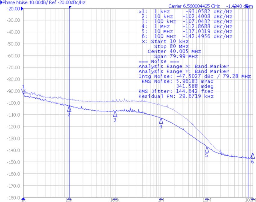
2712                                                                                IEEE JOURNAL OF SOLID-STATE CIRCUITS, VOL. 56, NO. 9, SEPTEMBER 2021

Fig. 2.     Behavioral model of the TA-assisted DMRO  FDC with the gain calibration technique details omitted.

16 dB. Additionally, it incorporates and is the first experimen-                    B. TA-Assisted DMRO  FDC Behavior
tal demonstration of several  FDC improvements proposed                              An analysis similar to that presented in [8] but modified to
in [9]. These improvements include an all-digital background                        include the TA and the improvements presented in [9] yields
gain calibration technique that simplifies the DMRO design,                         the  FDC behavioral model shown in Fig. 2. In this model,
and various architecture changes that relax the  FDC’s tim-                       JTA [n] is the TA’s output jitter during the nth reference period,
ing constraints. A modified delay-free asynchronous DMRO                            θPLL (t), θref (t), and θDMRO (t) are the respective phase errors
phase sampling scheme is also incorporated in the PLL to                            in cycles of v PLL (t), v ref (t), and the DMRO, τn , tn , ρn , and γn ,
further relax the  FDC’s timing constraints.                                      for n = 0, 1, 2, . . . , are the respective times of the nth rising
                                                                                    edges of v div (t), v ref (t), v TA (t), and v samp (t), Tref = 1/ f ref ,
                II. PLL H IGH -L EVEL A RCHITECTURE                                 and TPLL = 1/ f PLL .1 The behavioral model in Fig. 2 does not
A. PLL Overview                                                                     include error sources corresponding to the PFD, the MMD,
     A high-level block diagram of the PLL is shown in Fig. 1(a),                   or the divide-by-2 block. Simulations performed by the authors
where v ref (t) and v PLL (t) are the output waveforms of the                       indicate that these blocks do not significantly affect the PLL’s
reference oscillator and the PLL, respectively. Ideally, v PLL (t)                  phase noise, so they are omitted in the figure for simplicity.
is periodic with frequency fPLL = 2(N + α) fref , where fref                           The MMD is identical to those in analog PLLs, so, as illus-
is the reference frequency, N is a positive integer, and α is a                     trated in Fig. 2, τn is an accumulated version of 2TPLL (N −
fractional frequency offset that ranges from −1/2 to 1/2.                           v[n − 1]) plus noise, where 2TPLL is the divide-by-2 block’s
     The PLL consists of a TA-assisted DMRO  FDC, a dig-                          output period and N − v[n − 1] is the MMD modulus.
ital loop controller (DLC) with quantization noise cancellation                        As explained in Section III-B, the TA is implemented as a
(QNC), a digitally-controlled oscillator (DCO), and a divide-                       chain of NTA nominally identical delay cells. The propagation
by-2 block with output v div2 (t). The  FDC generates two                         delay of each delay cell is τfast when v ref (t) is low and
 f ref -rate digital sequences, y[n] and −êq [n]. Ideally                           τslow otherwise, where τfast < τslow . As also explained in
                                                                                    Section III-B, the TA delays the rising edges of v div (t) such
 y[n] = −α − ePLL [n] + eq [n] − 2eq [n − 1] + eq [n − 2], (1)                      that the pulse-width of the PFD output, u(t), during the nth
                                                                                    reference period, i.e., u n = ρn − tn , is given by
where ePLL [n] is a measure of the PLL’s average frequency
error over the nth reference period and eq [n] is  FDC                                        u n = −ATA (tn − τn ) + NTA τslow + JTA [n],                       (2)
quantization error [8], [9]. The sequence êq [n] is an estimate
of eq [n], and it is used to cancel most of the contribution of                     where
eq [n] prior to the digital loop filter (DLF) [7]–[12].
                                                                                                                 ATA = τslow /τfast                                (3)
   Fig. 1(a) and (1) imply that the DLF input, p[n], is a
measure of the PLL average phase error over the nth                                 is the TA gain and NTA τslow is a constant offset term introduced
reference period plus a first-order highpass shaped version of                      as a byproduct of the TA’s operation. Thus, the combined
the residual  FDC quantization error, eq [n] − êq [n]. The                        behavior of the TA and the PFD is equivalent to that of an
p[n] sequence is lowpass filtered by the DLF, the output of                         inverting amplifier with input tn − τn and additive noise and
which controls the DCO.                                                             offset terms.
   Fig. 1(b) shows a simplified block diagram of the                                     The DMRO is a ring of N R nominally identical delay
TA-assisted DMRO  FDC. It consists of a PFD, a DMRO,                              cells. Ideally, its frequency is f high when u(t) is high and
a digital ring phase calculator (RPC), a multi-modulus divider                       f low otherwise, where fhigh > f low . As explained in [8] and
(MMD), and a TA. The signal v samp (t), which is an inverted
version of v ref (t), is used within the RPC to sample the DMRO                       1 By definition, θ (t) is the phase error at time t of v (t) in units of cycles
                                                                                                         ref                                    ref
phase each reference period. The signal processing details of                       of v ref (t). Accordingly, Tref θref (t) has units of seconds and it represents the
                                                                                    reference oscillator’s absolute jitter. Similarly, θPLL (t) represents the phase
the RPC including the gain calibration technique are shown                          error at time t of v PLL (t) in units of cycles of v PLL (t), so TPLL θPLL (t) has
in Fig. 1(c) [9].                                                                   units of seconds and it represents the PLL output signal’s absolute jitter.

          Authorized licensed use limited to: Univ of Calif San Diego. Downloaded on September 08,2021 at 15:04:13 UTC from IEEE Xplore. Restrictions apply.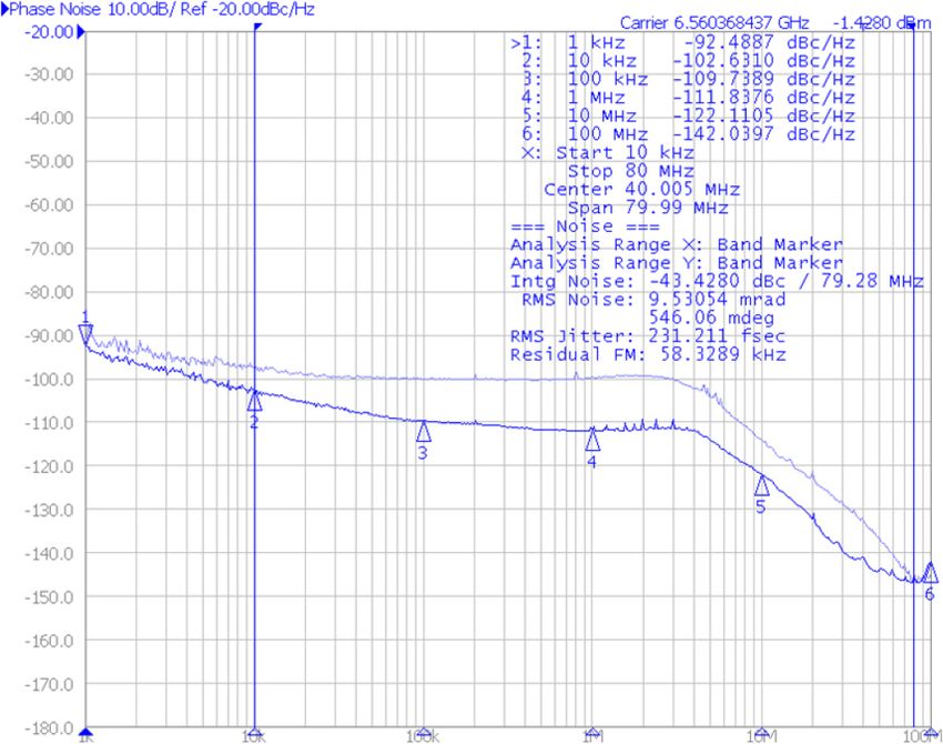
HELAL et al.: TA ASSISTED FDC BASED DIGITAL FRACTIONAL-N PLL                                                                                              2713

illustrated in Fig. 2, the behavior of the DMRO is that of an                     Unfortunately, these options are not attractive. In principle,
accumulator with gain                                                          increasing the widths of the transistors that make up the
                                                                               DMRO’s delay cells increases ADMRO via (4) and decreases
                      ADMRO = f high − f low                            (4)    the DMRO’s 1/ f 3 phase noise component by reducing tran-
followed by an additive noise source, an additive nflow Tref                   sistor flicker noise, but in practice ADMRO increases only up
term, and a quantizer, Q r , with quantization step-size                       to a point beyond which parasitic capacitances and supply
r = (2N R )−1 .                                                               resistance cause ADMRO to decrease with further transistor
   As explained in [9], the RPC extracts the information                       width increases. After this point, ADMRO can only be increased
encoded in the sampled and quantized DMRO phase and com-                       further by reducing the number of DMRO delay cells, N R .
putes a fixed-point measure of −α − ePLL [n] each reference                    Given that eqr [n] is proportional to r = (2NR )−1 , this would
period. This measure is quantized to the nearest integer to com-               reduce the effectiveness of QNC, which would require the PLL
pute y[n], and the resulting quantization error, êq [n], is used               bandwidth to be reduced to compensate for the increase in
within the DLC to perform QNC. This coarse quantization                        quantization noise power. Interestingly, increasing the number
operation is represented by a unity step-size quantizer, Q c ,                 of DMRO delay cells does provide a modest net benefit.
in Fig. 2.                                                                     For example, doubling N R reduces A2DMRO by 6 dB, but as
   An analysis similar to that presented in [9] shows that the                 shown in [13] it decreases the power of the DMRO’s 1/ f 3
DMRO locks to an average frequency of Mfref , and the average                  phase noise component by 9 dB. Hence, each doubling of N R
u(t) pulsewidth, Tu , is                                                       reduces the power contribution of the DMRO’s 1/ f 3 phase
                                                                               noise component to the PLL’s phase by 3 dB. Unfortunately,
                  Tū = A−1
                         DMRO (M − Tref f low ).                        (5)    achieving large phase noise reductions in this manner typically
                                                                               requires impractically large numbers of DMRO delay cells.
The parameter M is chosen so that the falling edges of
                                                                                  These tradeoffs are avoided in this work because the TA
u(t) occur between rising edges of v ref (t) and v samp (t), i.e.,
                                                                               provides amplification prior to the DMRO. As described
tn < ρn < γn for all n. This with the TA operation described
                                                                               above, the DMRO’s contribution to the PLL’s phase noise
in Section III-B causes the rising edges of v div (t) to precede
                                                                               is proportional to A−2 TA , so each doubling of A TA reduces the
the rising edges of v ref (t), i.e., τn < tn for all n, so that
                                                                               power of the DMRO’s contribution to the PLL’s phase noise
                   γn−1 < τn < tn < ρn < γn                             (6)    by 6 dB.
                                                                                  Both the TA and the DMRO are made up of dual-delay
when the PLL is locked.                                                        inverter based delay cells, but the TA is an open-loop chain
  A simplified version of the TA-assisted  FDC behavioral                    and the DMRO is a ring, so transistor flicker noise gives rise to
model that is valid for constant gn is shown within the                        1/ f noise in JTA [n] and 1/ f 3 noise in θDMRO(γn ). Nevertheless,
dashed contour in Fig. 2, wherein all noise components are                     as implied by Fig. 2, the contributions of JTA [n] and θDMRO(γn )
input-referred and lumped into ePLL [n], the offset components                 to y[n] are first-order and second-order highpass shaped,
are omitted, and the quantizers Q r and Q c are replaced by                    respectively, so flicker noise injected by each TA transistor
their respective additive error sequences, eqr [n] and êq [n]. The             has a similar contribution to the PLL’s phase noise as that
model implies that the behavior of the  FDC when                             injected by each DMRO transistor.
                                      1                                           Yet, it is not the case that using the TA simply transfers
                     gn =                                               (7)    the problem of reducing the effect of flicker noise from the
                             2TPLL ATA ADMRO
                                                                               DMRO to the TA. As implied by (3), ATA depends on a
is identical to that of a second-order  modulator, the output                ratio of inverter delays, so the TA’s flicker noise can be
of which is given by (1) with                                                  reduced by increasing transistor widths without significantly
                    eq [n] = gn eqr [n] + êq [n].                      (8)    decreasing ATA or incurring other side effects similar to those
                                                                               mentioned above that come with reducing the DMRO’s 1/ f 3
As explained in [9], when (7) is not satisfied, êq [n] is                      phase noise component. Furthermore, the TA is only active
imperfectly canceled by QNC so it leaks into the DLF input,                    for a fraction of each reference period, whereas the DMRO
thereby degrading the PLL’s phase noise. The gain calibration                  operates continuously. As the power of the noise introduced by
technique shown in Fig. 1(c) causes gn to converge to the right                a chain of inverters grows at least proportionally to the number
side of (7), which effectively circumvents this problem [9].                   of inverters that transition as explained in [13], it follows that
   It follows from Fig. 2 and (7) that the power contribution                  the TA noise contribution can be made small compared to that
of the DMRO’s phase noise to y[n], and, hence, to the PLL’s                    of the DMRO.
phase noise, is proportional to both A−2           −2
                                         TA and A DMRO . The                      For instance, in the implemented PLL, 100 TA delay cells
original DMRO  FDC PLL presented in [7] does not                             transition each reference period, whereas 660 DMRO delay
incorporate a TA, so it corresponds to the case of ATA = 1                     cells transition each reference period on average. Moreover,
in (7), and its in-band phase noise is dominated by the                        in contrast to the TA, each delay cell within the DMRO
DMRO’s 1/ f 3 phase noise component. In the absence of a                       transitions four to six times each reference period. Given that
TA, modifying the DMRO to increase ADMRO and/or reduce                         flicker noise changes slowly relative to Tref , having an edge
the DMRO’s 1/ f 3 phase noise component are the only options                   propagating four to six times through the same delay cell
that would have mitigated this problem.                                        effectively increases the power of the DMRO’s 1/ f 3 phase

     Authorized licensed use limited to: Univ of Calif San Diego. Downloaded on September 08,2021 at 15:04:13 UTC from IEEE Xplore. Restrictions apply.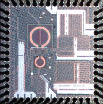
2714                                                                                IEEE JOURNAL OF SOLID-STATE CIRCUITS, VOL. 56, NO. 9, SEPTEMBER 2021

Fig. 3.     Block diagram of the PLL showing implementation details and the four different power domains in dashed boxes.

                                                                                    are in the  FDC’s digital sub-block to incorporate the
                                                                                    improvements proposed in [9] which include the gain calibra-
                                                                                    tion technique shown in Fig. 1(c). As explained in [9], the f ref -
                                                                                    rate multiplier prior to the RPC’s accumulator in Fig. 1(c)
                                                                                    represents most of the gain calibration technique’s added
                                                                                    complexity. Its inputs have respective bit-widths of 12 and
                                                                                    14 bits, and its output has a bit-width of 25 bits. The RPC’s
                                                                                    accumulator would have required 24 bits in the absence of the
                                                                                    multiplier, so the inclusion of the gain calibration technique
                                                                                    negligibly increases the power consumption and circuit area
                                                                                    of the RPC accumulator and subsequent digital sub-blocks.
Fig. 4. High-level block diagram of the PNR digital block and clocking              Furthermore, the relaxed timing of the implemented  FDC
scheme.                                                                             architecture relative to that presented in [7] causes the power
                                                                                    consumption and circuit area of the multiplier to be negligible
noise component by approximately 3-5 dB compared to the                             relative to those of the overall digital block.
case where the edge propagates through four to six different
delay cells. These features made it possible for the TA to                          A. Timing
suppress the DMRO’s contribution to the PLL’s phase noise                              As shown in the timing diagram of Fig. 5, the MMD loads
without the TA’s noise being a limitation.                                          its inputs, mod4 [n] and mod5 [n], 30TPLL after the rising edge
                                                                                    of v div (t). Fig. 5 implies that for the earliest possible v div (t)
                     III. I MPLEMENTATION D ETAILS                                  rising edge, the  FDC portion of the PNR digital block has
    The implemented PLL is shown in Fig. 3. It has four                             a time budget of about 51TPLL ∼     = ¾Tref to generate its outputs
power supply domains, which correspond to the dashed boxes                          after v rdy (t) goes high. This constraint is easy to satisfy in
in Fig. 3. The place-and-route (PNR) digital block is clocked                       practice as the  FDC logic does not require more than two
at a rate of f PLL /8 by v clk (t) and contains the DLC, the                        periods of v clk (t) (i.e., 16TPLL ) to compute the MMD inputs.
DCO control logic, the  FDC’s z −1 register, and all                              Accordingly, the implemented PLL has no significant timing
RPC components except the cycle counter and phase-sampling                          bottle-necks, which makes its implementation much simpler
flip-flops.                                                                         than that of prior  FDCs [7], [8], [12], [14], [15].
    As shown in Fig. 4, the PNR digital block comprises three
sub-blocks, FDC digital, DLC, and DCO digital, that are                             B. TA
clocked sequentially by gated versions of v clk (t). The signal                         Fig. 6(a) shows a conceptual block diagram of the proposed
v rdy (t) is timed such that it goes high once each reference                       TA. It consists of NTA nominally identical inverter based delay
period when the DMRO phase information is ready to be                               cells, where NTA is an even number. The delay of each delay
processed by the PNR digital block. The clkFDC , clkDLC , and                       cell, τdelay , takes on one of two values: τfast when v ref (t) is
clkDCO clock signals are generated by the flip-flop chain driven                    low and τslow when v ref (t) is high.
by v rdy (t), and the numbers of flip-flops between adjacent                            It follows from (6) that during the nth reference period,
clock signals are such that enough time is allocated for each                       the time, tn , of the rising edge of v ref (t) occurs after the time,
digital sub-block to meet digital timing constraints across PVT                     τn , of the corresponding rising edge of v div (t), but before
variations for an input clock frequency of 1 GHz.                                   the time, ρn , at which the rising edge of v div (t) finishes
    The details of the sub-blocks within the PNR digital block                      propagating through the TA. Therefore, at time τn , when the
are similar to those presented in [7]. Most of the differences                      rising edge of v div (t) starts propagating through the TA, the

          Authorized licensed use limited to: Univ of Calif San Diego. Downloaded on September 08,2021 at 15:04:13 UTC from IEEE Xplore. Restrictions apply.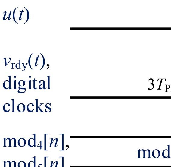
HELAL et al.: TA ASSISTED FDC BASED DIGITAL FRACTIONAL-N PLL                                                                                                   2715

Fig. 5.     PLL timing diagram.

delay cells have a delay of τfast . When v ref (t) goes high at
time tn , the rising edge of v div (t) has already propagated
through (tn − τn )/τfast  delay cells and a fraction, given
by (tn − τn )/τfast − (tn − τn )/τfast , of a delay cell. Thus,
at time tn , the rising edge of v div (t) has propagated through
an equivalent of (tn − τn )/τfast delay cells, including both
integer and fractional parts. At this time, the TA’s delay cells
are switched to have a delay of τslow , so the remaining TA
delay cells through which the edge must propagate contribute
a combined delay of (NTA − (tn − τn )/τfast )τslow . Consequently,
the time, ρn , at which v TA (t) goes high is given by

                   tn − τn                    tn − τn
     ρn = τn +              τfast + NTA −              τslow . (9)
                     τfast                      τfast
This implies that the pulse-width of u(t) during the nth
reference period, u n = ρn − tn , is given by (2) with ATA given
by (3), where the jitter term, JTA [n], represents the combined
effect of all transistor noise sources within the TA.
   It follows from the explanation above that for the TA to
provide time-difference amplification it is necessary to ensure:
                          0 < tn − τn < NTA τfast .                        (10)
Otherwise, the TA would only introduce a fixed delay between
v div (t) and v TA (t). Fig. 5 implies that the time at which
the MMD loads its inputs also imposes a constraint on the
maximum value of tn − τn . Specifically, the MMD must load
its inputs at the time of the rising edge of clkFDC at the earliest,
which can occur up to 37TPLL after the falling edge of v ref (t).
Therefore, tn − τn must satisfy
                         tn − τn < 1/2 Tref − 7TPLL                         (11)    Fig. 6. (a) Dual-delay inverter chain based TA concept, (b) details of TA unit
                                                                                    delay cell, and (c) illustration of τdelay versus tn for low-to-high and high-to
in addition to (10). Moreover, for the  FDC to work                               low input transition (not to scale for illustration purposes).
properly, u(t) must go low before the DMRO phase is sampled
at time γn , which requires                                                         inverter. When v ref (t) goes high, the tri-state inverter is dis-
                        0 < u n < 1/2Tref + 10TPLL.                        (12)     abled by disconnecting its ground and power supply terminals
                                                                                    from the supply rails, thereby increasing τdelay from τfast to
Equations (10)-(12) impose design constraints on the TA                             τslow .
parameters NTA , τslow , τfast , and ATA.                                              Ideally, τdelay changes instantaneously from τfast to τslow
  As shown in Fig. 6(b), each of the TA’s dual-delay inverters                      when v ref (t) goes high, in which case the TA performs linear
consists of a standard inverter in parallel with a larger tri-state                 amplification. Unfortunately, the τfast -to-τslow transitions are

          Authorized licensed use limited to: Univ of Calif San Diego. Downloaded on September 08,2021 at 15:04:13 UTC from IEEE Xplore. Restrictions apply.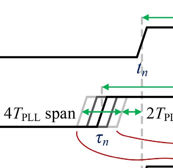
2716 IEEE JOURNAL OF SOLID-STATE CIRCUITS, VOL. 56, NO. 9, SEPTEMBER 2021
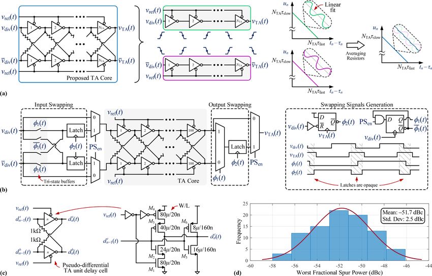
Fig. 7. Proposed TA core including the nonlinearity mitigation technique, (b) implemented TA architecture with PS mode, (c) TA unit delay cell circuit
details, and (d) histogram of the highest fractional spur power that results from the (simulated) TA’s unit delay cells’ random mismatches.
non-instantaneous in practice, which causes TA nonlinear- mode, the falling edge of v div (t) propagates through the TA
ity. Moreover, as illustrated in Fig. 6(c), this transition also each reference period. This resets the delay cells’ states for
depends on whether the cell’s input, dn−1 (t), goes from low the next rising edge of v div (t), but the power consumed by the
to high or vice versa. resulting delay cell transitions represents a significant portion
The TA topology shown in Fig. 7(a) is proposed to reduce of the TA’s total power consumption. The idea behind the
such nonlinearity. It consists of two nominally identical delay PS mode is to swap the differential inputs and swap the
chains in parallel, where the input of one delay chain is an differential outputs of the TA each reference period to obviate
inverted version of that of the other delay chain, both delay the need to reset the delay cells, so the falling edge of v div (t)
chains are controlled by v ref (t), and each pair of parallel delay can be prevented from propagating through the TA to save
cells are cross-connected with averaging resistors. As shown power.
in Fig. 7(a) for the top and bottom delay chains in isolation, The implemented TA, which includes the nonlinearity mit-
the odd-indexed and even-indexed delay cells have inputs that igation technique and PS mode option as described above,
transition in opposite directions, so they have different τfast - is shown in Fig. 7(b). It comprises the TA core shown
to-τslow transitions. This causes a quasi-periodic artifact in the in Fig. 7(a) as well as input and output swapping circuitry
input-output characteristics of the delay chains. Driving the used when the PS mode is enabled. The transistor-level
bottom delay chain by an inverted version of v div (t) causes its details of the TA’s delay cells are shown in Fig. 7(c). The
input-output characteristic to be shifted with respect to that of TA core was designed to maximize the value of ATA while
the top delay chain such that, when averaged via the cross- satisfying the constraints in (10)-(12). Specifically, NTA = 100,
coupled resistor network, the nonlinearity of the cross-coupled τfast = 10 ps, τslow = 70 ps, and ATA = 7. Simulation
delay chains is considerably smaller than that of either delay results predict that the TA’s gain varies by ±7% across
chain in isolation. Behavioral simulations of the PLL in which process corners, ±10% across process corners and temperature
the TA’s nonlinear behavior is considered and all other spur- variations (0 ◦ C to 85 ◦ C), and ±14% across process corners,
generation mechanisms are neglected suggest that the power of temperature variations, and supply voltage variations (±10%).
the PLL’s worst-case fractional spur decreases by 7 dB when The PS mode is enabled and disabled via the PSen sig-
the proposed nonlinearity mitigation technique is used. nal. When enabled, the φ1 (t) and φ2 (t) signals are used to
In addition to having improved linearity, the proposed implement the input and output swapping operations. The
TA topology’s pseudo-differential nature can be exploited to signal φ1 (t), which is derived from v div (t), is used to swap
implement a TA power-saving (PS) mode. Without the PS the inputs and the outputs of the TA core each reference
Authorized licensed use limited to: Univ of Calif San Diego. Downloaded on September 08,2021 at 15:04:13 UTC from IEEE Xplore. Restrictions apply.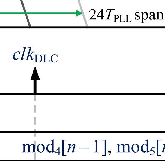
HELAL et al.: TA ASSISTED FDC BASED DIGITAL FRACTIONAL-N PLL                                                                                                   2717

Fig. 8.     DMRO and delay-free asynchronous phase sampling scheme details.

period, whereas φ2 (t) is used to control the input and output                      without the need for level-shifting. The ×2 inverter shown
latches. As illustrated in the timing diagram shown in Fig. 7(b),                   within the dashed box in Fig. 8 is used to buffer the delay
these latches prevent the falling edges of v div (t) from prop-                     cell’s input to reduce the disturbance to the DMRO when its
agating through the TA core, and also prevent the output                            phase is sampled.
swapping circuitry from disturbing v TA (t) while the swapping                           As explained in Section II-B, the TA causes the PLL
occurs.                                                                             phase noise contributed by the DMRO to be attenuated in
   The TA was laid out such that systematic mismatch among                          power by a factor of A2TA . Additionally, the DMRO’s 1/ f 3
its unit cells is negligible, and the unit cells are sized such that                phase noise component is further mitigated by using a large
the power of the PLL’s worst-case fractional spur caused by                         number of stages [13]. This comes at the expense of higher
random mismatches among the TA’s delay cells is approx-                             digital complexity and higher power consumption, primarily
imately −50 dBc. This was determined by performing a                                due to the charging and discharging of the gates controlled
Monte Carlo simulation in Cadence to obtain 90 different TA                         by u(t).
input-output characteristics, and the results were imported into                         To prevent the DMRO from running with multiple stages
a bit-exact, event-driven, custom behavioral PLL simulator.                         transitioning simultaneously, even for a brief period of time,
Fig. 7(d) shows a histogram of the simulated PLL’s worst-case                       the first delay cell includes a switch between the ground
fractional spur power. As shown in Fig. 7(d), the worst-case                        terminal of the ×1 inverter and the ground rail. At startup,
fractional spur power’s expected value is −51.7 dBc, and its                        both u(t) and the enable signal are set low. This opens the
standard deviation is 2.5 dBc.                                                      ring so that any transition propagating through it eventually
   As mentioned in Section I, the proposed TA achieves                              reaches the first stage and stops propagating. The switch is
better noise performance than a comparably configured TA                            subsequently closed after which the DMRO operates normally.
of the type presented in [6]. One reason for this difference                             The DMRO phase sampling scheme is shown in Fig. 8.
is that the TA in [6] incorporates two ring oscillators that                        As explained below, it addresses the issue that the sampling
both contribute noise to the output whereas the proposed TA                         clock, v samp (t), and the DMRO are asynchronous yet avoids
incorporates a single delay-chain that contributes noise to the                     the delay incurred by the DMRO sampling scheme in [7].
output. Another reason is that the TA presented in [6] requires                     It consists of a cycle counter followed by sampling flip-flops
NAND gate based delay cells instead of inverter based delay                         and a phase decoder. The principle behind the sampling of
cells which each introduce more phase noise than comparable                         the cycle counter’s outputs is based on that of the asynchro-
inverter based delay elements.                                                      nous sampling schemes presented in [16] and [17]. To the
                                                                                    knowledge of the authors, the proposed phase decoder imple-
                                                                                    mentation described below is introduced for the first time in
C. DMRO and Phase Sampling Scheme                                                   this work.
    The DMRO, which is shown in Fig. 8, consists of                                      The cycle counter consists of two 4-bit counters that are
N R = 127 inverter delay cells and has ADMRO = 670 MHz                              clocked, respectively, by the rising and falling edges of the
( f high = 730 MHz and f low = 60 MHz). Each DMRO delay                             DMRO delay cell with output d1 (t). On each rising edge of the
cell contains a dual-delay inverter that is similar to that used                     f ref -rate signal v samp (t), the counter outputs cpos (t) and cneg (t)
in the TA. It includes a standard ×1 inverter in parallel with                      are sampled to generate cpos [n] and cneg [n], and the DMRO
a ×16 tri-state inverter, and the tri-state inverter’s power and                    outputs d1 (t), d2 (t), . . . , d127 (t) are sampled to generate d1 [n],
ground lines are connected to or disconnected from the supply                       d2 [n], . . . , d127 [n]. The phase decoder consists of a lookup
rails when u(t) is high or low, respectively. This modulates                        table (LUT) that quantizes the sampled DMRO outputs to a
each delay cell’s propagation delay such that the DMRO                              10-bit sequence, tR [n], which represents the fractional part of
frequency is fhigh when u(t) is high and f low when u(t) is                         the sampled DMRO phase, and logic that computes cR [n],
low. In both cases, the DMRO outputs swing from rail to rail,                       which represents the integer part of the sampled DMRO phase.
which allow the DMRO outputs to drive standard digital logic                        The number of bits of tR [n] was chosen to ensure that the

          Authorized licensed use limited to: Univ of Calif San Diego. Downloaded on September 08,2021 at 15:04:13 UTC from IEEE Xplore. Restrictions apply.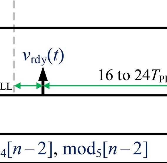
2718                                                                                IEEE JOURNAL OF SOLID-STATE CIRCUITS, VOL. 56, NO. 9, SEPTEMBER 2021

                                                                                    Fig. 10.   Die photograph.
Fig. 9.     MMD block diagram with example timing diagram.
                                                                                                                       TABLE I
                                                                                                    A REA AND P OWER B REAKDOWN OF THE IC
contribution to the PLL’s phase noise from the error introduced
by the LUT’s quantization operation is negligible compared to
those of the other error sources.
   The top and bottom counters in the cycle counter are
clocked when tR [n] ∼   = 0 and tR [n] ∼  = 126r , respectively,
where r = 1/254. Hence, tR [n] can be used to determine
which counter output was not changing when the sampling
event occurred. As shown in Fig. 8, whenever tR [n] is between
63r and 189r , cR [n] is set to cpos [n]. Ideally, cR [n] should
be set to cneg [n] when tR [n] is between 190r and 253r , and
to cneg [n] + 1 when tR [n] is between 0 and 62r , so as to                           When the FSM’s psel (t) output bit is low, the prescaler
account for the bottom counter being clocked half a DMRO                            divides by 4. Otherwise, it divides by 5. At the beginning
cycle after the top counter is clocked. Yet to work correctly                       of each MMD cycle, the FSM sets psel (t) low for five periods
this would require cpos (0) = cneg (0) and the initial DMRO                         of v pres (t), so the first five periods of v pres (t) each have a
fractional phase to be such that the top counter is clocked                         duration of four v div2 (t) periods. Then, the FSM sets psel (t)
before the bottom counter after startup, which are hard to                          so that mod4 [n] counts to 4 followed by mod5 [n] counts to 5
ensure in practice.                                                                 occur, where
   These requirements are avoided via the ccorr [n] correction
                                                                                     mod5 [n] = N − v[n] − 20 − 4(N − v[n] − 20)/4 and
logic shown in Fig. 8. As both sampled counter outputs are
reliable when tR [n] is around 63r and 190r , the ccorr [n]                        mod4 [n] = (N − v[n] − 20)/4 − mod5 [n],                                (14)
logic block in Fig. 8 computes                                                      after which N − v[n] periods of v div2 (t) will have occurred.
           ⎧                                                                           As illustrated in the timing diagram shown in Fig. 9 for the
           ⎪
           ⎨ cpos [n] − cneg [n] − 1, if tR [n] ∈ [53r , 73r],                    example case of mod5 [n] = 1, the FSM’s ppass(t) output goes
ccorr [n] = cpos [n] − cneg [n],      if tR [n] ∈ [180r , 200r ],
           ⎪
           ⎩                                                                        high at the start of the last full v pres (t) period prior to the next
             ccorr [n − 1],           otherwise,                                    rising edge of v div (t), which causes the edge-select flip-flop’s
                                                               (13)                 output to go high on the next rising edge of v pres (t). The resyn-
                                                                                    chronization flip-flop samples the edge-select flip-flop output
and cR [n] is set to cneg [n] + ccorr [n] when tR [n] is between                    on the next rising edge of v div2 (t) to prevent the MMD output
190r and 253r , to cneg [n] + ccorr [n] + 1 when tR [n] is                        edge from being corrupted by noise and modulus-dependent
between 0 and 62r , and to cpos [n] otherwise.                                     delay error that originated in the prior MMD components.
                                                                                       All MMD blocks were built using standard cells, with
D. MMD                                                                              the exception of the resynchronization flip-flop which was
                                                                                    custom-designed to minimize its contribution to the PLL’s
   As shown in Fig. 9, the MMD consists of a finite-
                                                                                    phase noise.
state machine (FSM), a 4/5 prescaler, an edge-select flip-
flop, and a resynchronization flip-flop. As explained below,
the MMD causes the rising edges of v div (t) during the nth and                     E. DCO
(n + 1)th reference periods to be separated by N − v[n]                               The DCO is similar to that presented in [7]. It consists
periods of v div2 (t).                                                              of a single-turn center-tapped inductor, a cross-coupled pair

          Authorized licensed use limited to: Univ of Calif San Diego. Downloaded on September 08,2021 at 15:04:13 UTC from IEEE Xplore. Restrictions apply.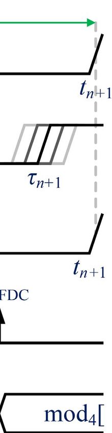
HELAL et al.: TA ASSISTED FDC BASED DIGITAL FRACTIONAL-N PLL                                                                                               2719

Fig. 11.   Measured PLL phase noise at f PLL = 6.56 GHz with and without the TA enabled for (a) 1-MHz bandwidth and (b) 4.5-MHz bandwidth.

of nMOS transistors, a tail resonant tank of the type pro-                      a post-layout extraction tool flaw. Removing metal near the
posed in [18], a triode MOS transistor tail source, an integer                  DCO’s main inductor via focused ion beam (FIB) surgery
frequency control element (FCE) bank driven by cI [ p], and                     made the DCO functional, but even with its maximum current
a fractional FCE bank driven by cF [ p]. The implemented                        setting and its supply set to 0.9 V, its oscillation amplitude is
FCEs are of the type presented in [15], and the minimum-size                    extremely low. Consequently, the DCO’s power consumption
FCE has an equivalent frequency step of min = 160 kHz                          is that of a high-performance DCO, yet it achieves relatively
at 6.5 GHz. The DCO’s 16-bit input sequence, d[n], is split                     poor phase noise performance (e.g., 10 dB worse at a 1-MHz
into integer and fractional parts. The integer part is encoded                  offset than expected2) and its low oscillation amplitude makes
to drive the integer FCE bank, which comprises eight 32min                     it highly sensitive to interference from other circuit blocks.
FCEs and five pairs of 16min , 8min , 4min , 2min , and min                While the PLL’s overall measured performance is nevertheless
FCEs. The fractional part is up-sampled and re-quantized by a                   in line with the current state of the art, these issues limited
second-order  modulator that generates a five-level output                    its performance as quantified later in this section. The IC’s
sequence. This output sequence is scrambled by a dynamic                        measured output power is around −34 dBm, so an amplifier
element matching (DEM) encoder, the outputs of which drive                      module was used to boost the output power to around −2 dBm.
four min FCEs within the fractional FCE bank. The PLL                              Fig. 11 shows the measured phase noise of the PLL at
controls the DCO over a range of 41 MHz with a minimum                           f PLL = 6.5 GHz with and without the TA enabled for PLL
step size of 625 Hz.                                                            bandwidths of 1 and 4.5 MHz. The integrated random jitter
   The DCO also contains a binary-weighted capacitor array                      (i.e., the jitter omitting spurious tones), σRJ , is also reported
controlled via a serial peripheral interface (SPI), which                       in Fig. 11, where the integration band extends from 10 kHz
is in parallel with the integer and fractional FCE banks.                       to 80MHz. To estimate the expected noise reduction when the
The capacitor array has 7 bits of tuning over a frequency range                 TA is enabled, ATA was calculated indirectly from (7) using
of 5.6-6.6 GHz.                                                                 measured values of gn read through the SPI. It was found
                                                                                that gn converged to about 0.758 and 4.832 with and without
                   IV. M EASUREMENT R ESULTS                                    the TA enabled, respectively, with which two equations based
                                                                                on (7) were solved to find ATA = 6.37. This suggests that
   The prototype IC contains the PLL in Fig. 3 as well as an                    the TA reduces the power of the portions of the PLL’s phase
SPI port and test circuitry to measure internal signals during                  noise contributed by both the DMRO’s circuit noise and its
testing. It was fabricated in the GlobalFoundries 22-nm CMOS                    quantization noise by 16 dB.
22FDX technology. A die photograph is shown in Fig. 10,                             In the case of Fig. 11(a), the in-band spot phase noise
and area and power breakdowns are presented in Table I. The                     at a 100-kHz offset frequency decreases from −99 to
IC is packaged in a QFN28 package with a ground paddle                          −107 dBc/Hz when the TA is enabled, whereas in the case
and was tested with an Ironwood SG-MLF-7003 compression                         of Fig. 11(b), the in-band spot phase noise at a 1-MHz offset
elastomer socket. Except where noted otherwise, all of the                      frequency decreases from −100 to −112 dBc/Hz when the
measurements presented below were taken with a common                           TA is enabled. In the former case, the PLL’s in-band phase
set of PLL parameters set via the SPI.                                          noise has comparable contributions from the DMRO, reference
   Unfortunately, the DCO tank’s quality factor is severely
degraded by a layout issue to the point that the DCO                              2 The spot phase noises of the DCO after the FIB surgery when tuned to
as-fabricated does not even oscillate, and the problem was                      6.5 GHz are −59, −117, and −148 dBc/Hz at offset frequencies of 10 kHz,
not flagged by simulations prior to fabrication because of                      1 MHz, and 100 MHz, respectively.

      Authorized licensed use limited to: Univ of Calif San Diego. Downloaded on September 08,2021 at 15:04:13 UTC from IEEE Xplore. Restrictions apply.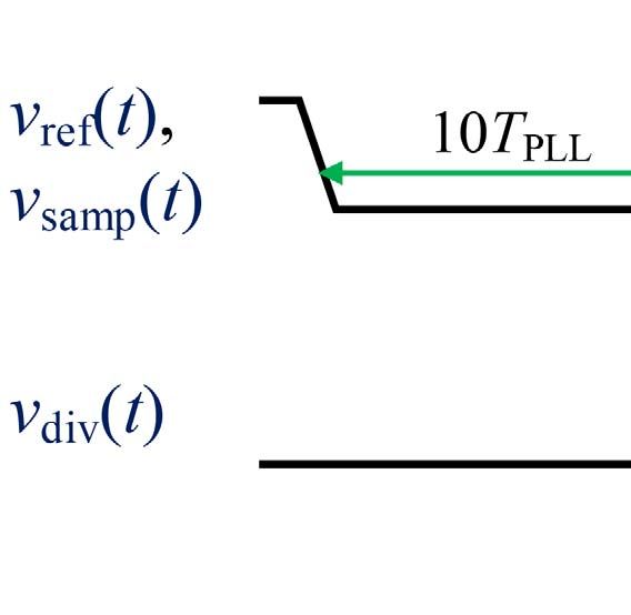
2720                                                                              IEEE JOURNAL OF SOLID-STATE CIRCUITS, VOL. 56, NO. 9, SEPTEMBER 2021

                                                                                  Fig. 14.   Representative PLL output spectrum.

Fig. 12. Measured PLL phase noise at f PLL = 6.56 GHz with the TA enabled
for out-of-band fractional spurs at 18-MHz offset frequency.

                                                                                  Fig. 15. PLL phase noise with and without gain calibration (GC) enabled
                                                                                  for a 4.5 MHz bandwidth.

                                                                                  swept such that α fref ranges from 1 kHz to 40 MHz with 20
                                                                                  equally-spaced values per decade on a log scale. The integra-
Fig. 13. (a) Largest measured fractional spurious tone and (b) total integrated   tion band of the jitter extends from 10 kHz to 80 MHz to
jitter (σTJ ) as a function of the fractional frequency.                          include all significant spurs. The spur powers were measured
                                                                                  with the spectrum analyzer’s averaging option disabled, and
signal, and DCO, whereas in the latter case, the in-band                          for each value of α, the instrument was configured to ensure
phase noise is mostly dominated by the DMRO phase noise.                          that five negative and positive fractional spur harmonics were
Accordingly, as the TA suppresses the DMRO’s contribution                         always visible. In each case, the largest fractional spur was one
to the PLL’s phase noise, the PLL’s in-band spot phase                            of the first three harmonics of α fref , and was no higher than
noise reduction is more significant in Fig. 11(b). Nonetheless,                   –49 dBc. The measured worst-case spurious tone powers are
as shown in Fig. 11(a), the spot phase noise at a 1-MHz offset                    in line with those predicted by simulation results that include
frequency decreases from −100 to −112 dBc/Hz when the                             random mismatches among the TA delay cells.
TA is enabled, which occurs because the PLL’s phase noise                            For some values of α fref > 5 MHz, spurs with power
is dominated by DMRO quantization error around that offset                        lower than −60 dBc and frequencies that are not multiples
frequency.                                                                        of α fref were measured. The authors have not definitively
   Fig. 12 shows the PLL’s measured phase noise with α fref                       determined the origin of these spurs, but suspect they are
set to 18 MHz, the PLL bandwidth set to 1 MHz, and the TA                         from external interference that is parasitically coupled into the
enabled. In this case, the integrated total jitter (i.e., the jitter              DCO and their effect is exacerbated by the DCO’s abnormally
including spurious tones), σTJ , was 151 fsrms . This represents                  low amplitude. These interference spurs are not reported
the best-case total jitter because it corresponds to a case where                 in Fig. 13(a), although their contribution to σTJ is taken into
the spurious tones are well outside the PLL bandwidth.                            account in Fig. 13(b), which is why σTJ increases somewhat
   The largest measured fractional spur and σTJ versus α fref                     for α fref > 5 MHz.
are shown in Fig. 13(a) and Fig. 13(b), respectively, for a PLL                      As shown in Fig. 14, the measured reference spur power is
bandwidth of 1 MHz. The fractional frequency offset, α, was                       lower than −80 dBc. As mentioned above, the authors believe

       Authorized licensed use limited to: Univ of Calif San Diego. Downloaded on September 08,2021 at 15:04:13 UTC from IEEE Xplore. Restrictions apply.
HELAL et al.: TA ASSISTED FDC BASED DIGITAL FRACTIONAL-N PLL 2721
TABLE II
P ERFORMANCE S UMMARY AND C OMPARISON TABLE
that the DCO’s low oscillation amplitude makes it extremely the analog domain to the DCO, again because of the DCO’s
sensitive to external interference. This theory is supported low oscillation amplitude.
by the observation that increasing the DCO supply, which Table II summarizes the performance of the PLL with and
increases its oscillation amplitude somewhat, tends to reduce without the TA PS mode enabled, along with that of the
the measured spurs. For example, measurements taken with the best digital PLLs published to date [7], [19]–[27]. As shown
DCO supply set to 1.1 V yields a reference spur of −85 dBc. in Table II, the PLL achieves one of the best in-band spot
Accordingly, the reported reference spur power in Fig. 14 is phase noises, and its spurious tone performance is comparable
a worst-case bound on the reference spur performance of the to that of other state-of-the-art digital PLLs, even though
PLL, as the power of this spur is expected to decrease when no dedicated spur mitigation technique is used. In contrast,
the DCO problem mentioned above is fixed in a future version automatic time-to-digital converter (TDC) gain tracking is
of the PLL. used to reduce the fractional spur from −35 to −55 dBc
Fig. 15 shows the measured phase noise of the PLL with in [22], a TDC calibration technique is used to reduce the
and without the gain calibration technique enabled for a PLL fractional spur power from −43 to below −74 dBc in [21],
bandwidth of 4.5 MHz. The results demonstrate the effect of and a phase interpolation nonlinearity calibration technique is
non-ideal FDC forward path gain, i.e., the effect of gn not used to reduce the fractional spur from −24.58 to −53.1 dBc
satisfying (7), on the PLL’s performance at high bandwidth in [20]. Similarly, digital-to-time converter (DTC) range reduc-
settings. As indicated in Fig. 15, the spot phase noise at a tion techniques are used in [19], [24], and [25] to improve
20-MHz offset frequency decreases by 32 dB when enabling fractional spur performance.
the gain calibration technique, which causes σTJ to decrease The PLL’s best-case σTJ is lower than most of the other
from 2.7 psrms to 248 fsrms . PLLs in Table II, but its power consumption is higher than
Measurements indicate that enabling the TA PS mode has those of the other PLLs. As previously mentioned, the imple-
several effects: 1) it decreases the PLL’s power consumption mented DCO consumes the power of a DCO with much
by 1.45 mW, which corresponds to 37% of the TA power better phase noise. Simulations run by the authors suggest
consumption when the PS mode is disabled, 2) it increases that for a properly designed DCO with similar phase noise to
the best-case σTJ by 20 fs because the swapping circuitry that of the implemented DCO, the power consumption should
shown in Fig. 7(b) introduces noise into the reference path, be around 4 mW instead of 8.75 mW. Alternatively, if the
3) it decreases the worst-case σTJ by 30 fs due to the slightly DCO had performed as expected, the PLL’s best-case σTJ
better fractional spur performance, and 4) it increases the would have been 115 fsrms instead of 151 fsrms . Furthermore,
reference spur power by 14 dB. The authors believe that as mentioned in Section III, the PNR digital was overdesigned
the reference spur power increase is related to coupling from to be clocked at 1 GHz, which is supported by measurements
Authorized licensed use limited to: Univ of Calif San Diego. Downloaded on September 08,2021 at 15:04:13 UTC from IEEE Xplore. Restrictions apply.2722 IEEE JOURNAL OF SOLID-STATE CIRCUITS, VOL. 56, NO. 9, SEPTEMBER 2021
given that the digital domain power supply can be reduced [11] E. Temporiti, G. Albasini, I. Bietti, R. Castello, and M. Colombo,
from 0.8 to 0.55 V without affecting the PLL’s performance. “A 700-kHz bandwidth fractional synthesizer with spurs compen-
sation and linearization techniques for WCDMA applications,” IEEE
In this case, the power consumption of the PNR digital goes J. Solid-State Circuits, vol. 39, no. 9, pp. 1446–1454, Sep. 2004.
down from 4.76 to 2.66 mW. Therefore, the implemented [12] C. Venerus and I. Galton, “Quantization noise cancellation for FDC-
PLL’s power consumption is higher than necessary, and it based fractional-N PLLs,” IEEE Trans. Circuits Syst. II, Exp. Briefs,
vol. 62, no. 12, pp. 1119–1123, Dec. 2015.
could potentially be lowered by approximately 6.85 mW. [13] A. A. Abidi, “Phase noise and jitter in CMOS ring oscillators,” IEEE
Nonetheless, as shown in Table II, even with the J. Solid-State Circuits, vol. 41, no. 8, pp. 1803–1816, Aug. 2006.
higher-than-necessary digital power consumption and worst- [14] C. Venerus and I. Galton, “Delta-sigma FDC based fractional-N PLLs,”
IEEE Trans. Circuits Syst. I, Reg. Papers, vol. 60, no. 5, pp. 1274–1285,
than-expected DCO performance, the PLL achieves a Gao May 2013.
figure of merit (FoM) comparable to or better than prior-art [15] C. Venerus and I. Galton, “A TDC-free mostly-digital FDC-PLL fre-
digital PLLs [28]. Had the DCO performed as expected, i.e., quency synthesizer with a 2.8-3.5 GHz DCO,” IEEE J. Solid-State
Circuits, vol. 50, no. 2, pp. 450–463, Feb. 2015.
with performance comparable to that of the DCO presented [16] J. Daniels, W. Dehaene, and M. Steyaert, “All-digital differential
in [7], the PLL’s best-case FoM would have been −245.1 dB VCO-based A/D conversion,” in Proc. IEEE Int. Symp. Circuits Syst.,
and −245.4 dB with and without the TA PS mode disabled, May 2010, pp. 1085–1088.
[17] M. Baert and W. Dehaene, “A 5-GS/s 7.2-ENOB time-interleaved VCO-
respectively. Alternatively, had the PLL’s power consumption based ADC achieving 30.5 fJ/cs,” IEEE J. Solid-State Circuits, vol. 55,
be 6.85 mW lower as explained above, the PLL’s best-case no. 6, pp. 1577–1587, Jun. 2020.
FoM would have been −244.3 dB and −243.7 dB with and [18] E. Hegazi, H. Sjoland, and A. A. Abidi, “A filtering technique to lower
LC oscillator phase noise,” IEEE J. Solid-State Circuits, vol. 36, no. 12,
without the TA PS mode disabled, respectively. pp. 1921–1930, Dec. 2001.
[19] A. Elkholy, T. Anand, W.-S. Choi, A. Elshazly, and P. K. Hanumolu,
“A 3.7 mW low-noise wide-bandwidth 4.5 GHz digital fractional-N PLL
ACKNOWLEDGMENT using time amplifier-based TDC,” IEEE J. Solid-State Circuits, vol. 50,
The authors are grateful to Colin Weltin-Wu, Yiwu Tang, no. 4, pp. 867–881, Apr. 2015.
[20] M. Heo, S. Bae, J. Lee, C. Kim, and M. Lee, “Quantizer-less pro-
and Dongmin Park for helpful advice, Raghavendra Haresamu- portional path fractional-N digital PLL with a low-power high-gain
dram for his constant support with different software tools, time amplifier and background multi-point spur calibration,” in Proc.
Julian Puscar and Mahmoud Abdellatif for digital-flow advice, 43rd IEEE Eur. Solid State Circuits Conf. (ESSCIRC), Sep. 2017,
pp. 147–150.
Prof. Gabriel Rebeiz for the use of his Signal Source Analyzer, [21] C.-W. Yao et al., “A 14-nm 0.14-psrms fractional-N digital PLL with a
Roddy Cruz for FIB support, Mohammed Salah El-Hadri for 0.2-ps resolution ADC-assisted coarse/fine-conversion chopping TDC
and TDC nonlinearity calibration,” IEEE J. Solid-State Circuits, vol. 52,
the die photograph, and Tom McKay and Global Foundries for no. 12, pp. 3446–3457, Dec. 2017.
IC fabrication, process design kit (PDK) support, and helpful [22] D. Liao, H. Wang, F. F. Dai, Y. Xu, R. Berenguer, and S. M. Hermoso,
advice. “An 802.11a/b/g/n digital fractional-N PLL with automatic TDC lin-
earity calibration for spur cancellation,” IEEE J. Solid-State Circuits,
vol. 52, no. 5, pp. 1210–1220, May 2017.
R EFERENCES [23] Z. Xu, M. Miyahara, K. Okada, and A. Matsuzawa, “A 3.6 GHz low-
noise fractional-N digital PLL using SAR-ADC-based TDC,” IEEE
[1] A. M. Abas, A. Bystrov, D. J. Kinniment, O. V. Maevsky, G. Russell, J. Solid-State Circuits, vol. 51, no. 10, pp. 2345–2356, Oct. 2016.
and A. V. Yakovlev, “Time difference amplifier,” Electron. Lett., vol. 38, [24] Y. Wu, M. Shahmohammadi, Y. Chen, P. Lu, and R. B. Staszewski,
no. 23, pp. 1437–1438, Nov. 2002. “A 3.5–6.8-GHz wide-bandwidth DTC-assisted fractional-N all-digital
[2] M. A. Abas, G. Russell, and D. J. Kinniment, “Design of sub-10- PLL with a MASH -TDC for low in-band phase noise,” IEEE
picoseconds on-chip time measurement circuit,” in Proc. Design, Autom. J. Solid-State Circuits, vol. 52, no. 7, pp. 1885–1903, Jul. 2017.
Test Eur. Conf. Exhib., Feb. 2004, pp. 804–809. [25] L. Bertulessi, L. Grimaldi, D. Cherniak, C. Samori, and S. Levantino,
[3] M. Lee and A. A. Abidi, “A 9 b, 1.25 ps resolution coarse–fine time-to- “A low-phase-noise digital bang-bang PLL with fast lock over a wide
digital converter in 90 nm CMOS that amplifies a time residue,” IEEE lock range,” in IEEE Int. Solid-State Circuits Conf. (ISSCC) Dig. Tech.
J. Solid-State Circuits, vol. 43, no. 4, pp. 769–777, Apr. 2008. Papers, Feb. 2018, pp. 252–254.
[4] S. Lee, Y. Seo, H. Park, and J. Sim, “A 1 GHz ADPLL with a 1.25 [26] X. Gao et al., “9.6 A 2.7-to-4.3 GHz, 0.16 psrms -jitter,-246.8 dB-FOM,
ps minimum-resolution sub-exponent TDC in 0.18 μm CMOS,” IEEE digital fractional-N sampling PLL in 28 nm CMOS,” in IEEE Int. Solid-
J. Solid-State Circuits, vol. 45, no. 12, pp. 2874–2881, Dec. 2010. State Circuits Conf. (ISSCC) Dig. Tech. Papers, Jan. 2016, pp. 174–175.
[5] S. Mandai, T. Iizuka, T. Nakura, M. Ikeda, and K. Asada, “Time-to- [27] Z. Chen et al., “14.9 sub-sampling all-digital fractional-N frequency
digital converter based on time difference amplifier with non-linearity synthesizer with–111dBc/Hz in-band phase noise and an FOM of
calibration,” in Proc. IEEE Eur. Solid-State Circuits Conf. (ESSCIRC), −242dB,” in IEEE Int. Solid-State Circuits Conf. (ISSCC) Dig. Tech.
Sep. 2010, pp. 266–269. Papers, Feb. 2015, pp. 1–3.
[6] B. Kim, H. Kim, and C. H. Kim, “An 8bit, 2.6 ps two-step TDC in 65 nm [28] X. Gao, E. A. M. Klumperink, P. F. J. Geraedts, and B. Nauta, “Jitter
CMOS employing a switched ring-oscillator based time amplifier,” in analysis and a benchmarking figure-of-merit for phase-locked loops,”
Proc. IEEE Custom Integr. Circuits Conf. (CICC), Sep. 2015, pp. 1–4. IEEE Trans. Circuits Syst. II, Exp. Briefs, vol. 56, no. 2, pp. 117–121,
[7] C. Weltin-Wu, G. Zhao, and I. Galton, “A 3.5 GHz digital fractional-PLL Feb. 2009.
frequency synthesizer based on ring oscillator frequency-to-digital con-
version,” IEEE J. Solid-State Circuits, vol. 50, no. 12, pp. 2988–3002, Eslam Helal received the B.Sc. (Hons.) and M.Sc.
Dec. 2015. degrees in electrical engineering from Ain Shams
[8] C. Weltin-Wu, E. Familier, and I. Galton, “A linearized model for the University (ASU), Cairo, Egypt, in 2014 and 2018,
design of fractional-N digital PLLs based on dual-mode ring oscillator respectively. He is currently pursuing the Ph.D.
FDCs,” IEEE Trans. Circuits Syst. I, Reg. Papers, vol. 62, no. 8, degree with the University of California at San
pp. 2013–2023, Aug. 2015. Diego, San Diego, CA, USA.
[9] E. Alvarez-Fontecilla, A. I. Eissa, E. Helal, C. Weltin-Wu, and I. Galton, From 2014 to 2018, he was a part-time Analog
“Delta-sigma FDC enhancements for FDC-based digital fractional- Design Engineer with Si-Ware Systems (now
N PLLs,” IEEE Trans. Circuits Syst. I, Reg. Papers, early access, Goodix Technology), Cairo. He was a Teaching and
Dec. 21, 2020, doi: 10.1109/TCSI.2020.3040346. Research Assistant with the Electronics and Com-
[10] S. Pamarti, L. Jansson, and I. Galton, “A wideband 2.4-GHz delta-sigma munications Engineering Department, ASU. His
fractional-NPLL with 1-Mb/s in-loop modulation,” IEEE J. Solid-State research interests include analog/mixed-signal integrated circuits and systems,
Circuits, vol. 39, no. 1, pp. 49–62, Jan. 2004. frequency synthesizers, and data converters.
Authorized licensed use limited to: Univ of Calif San Diego. Downloaded on September 08,2021 at 15:04:13 UTC from IEEE Xplore. Restrictions apply.HELAL et al.: TA ASSISTED FDC BASED DIGITAL FRACTIONAL-N PLL 2723
Enrique Alvarez-Fontecilla received the B.Sc. and Ian Galton (Fellow, IEEE) received the B.Sc.
M.Sc. degrees in electrical engineering from the Uni- degree from Brown University, Providence, RI,
versidad Católica de Chile (PUC), Santiago, Chile, USA, in 1984, and the M.S. and Ph.D. degrees from
in 2011 and 2013, respectively. He is currently the California Institute of Technology, Pasadena,
pursuing the Ph.D. degree with the University of CA, USA, in 1989 and 1992, respectively, all in
California at San Diego, San Diego, CA, USA. electrical engineering.
From 2012 to 2015, he was an Adjunct Assistant Since 1996, he has been a Professor of Electri-
Professor with the School of Engineering and also cal Engineering with the University of California
with the Institute of Philosophy, PUC. at San Diego, San Diego, CA, where he teaches
and conducts research in the field of mixed-signal
integrated circuits and systems for communications.
His research involves the invention, analysis, and integrated circuit implemen-
Amr I. Eissa received the B.Sc. (Hons.) and M.Sc.
tation of critical communication system blocks such as data converters and
degrees in electrical engineering from Ain Shams
phase-locked loops.
University (ASU), Cairo, Egypt, in 2012 and 2016,
respectively. He is currently pursuing the Ph.D.
degree in electronic circuits and systems with the
University of California at San Diego, San Diego,
CA, USA.
From 2013 to 2016, he was a Teaching and
Research Assistant with Electronics and Com-
munications Engineering Department, ASU. His
research interests include the analysis and design of
analog/mixed-signal integrated circuits and systems.
Authorized licensed use limited to: Univ of Calif San Diego. Downloaded on September 08,2021 at 15:04:13 UTC from IEEE Xplore. Restrictions apply.You can also read