Embedding of Ultrathin Chips in Highly Flexible, Photosensitive Solder Mask Resist
←
→
Page content transcription
If your browser does not render page correctly, please read the page content below
micromachines

Article
Embedding of Ultrathin Chips in Highly Flexible,
Photosensitive Solder Mask Resist
Florian Janek 1,2, * , Nadine Eichhorn 1 , Sascha Weser 1 , Kerstin Gläser 1 , Wolfgang Eberhardt 1
and André Zimmermann 1,2

                                          1   Hahn-Schickard, Allmandring 9B, 70569 Stuttgart, Germany; Nadine.Eichhorn@hahn-schickard.de (N.E.);
                                              Sascha.Weser@hahn-schickard.de (S.W.); Kerstin.Glaeser@hahn-schickard.de (K.G.);
                                              Wolfgang.Eberhardt@hahn-schickard.de (W.E.); Zimmermann@ifm.uni-stuttgart.de (A.Z.)
                                          2   Institute for Micro Integration (IFM), University of Stuttgart, Allmandring 9B, 70569 Stuttgart, Germany
                                          *   Correspondence: Janek@ifm.uni-stuttgart.de; Tel.: +49-711-685-83803

                                          Abstract: This work presents an embedding process for ultrathin silicon chips in mechanically
                                          flexible solder mask resist and their electrical contacting by inkjet printing. Photosensitive solder
                                          mask resist is applied by conformal spray coating onto epoxy bonded ultrathin chips with a daisy
                                          chain layout. The contact pads are opened by photolithography using UV direct light exposure.
                                          Circular and rectangular openings of 90 µm and 130 µm diameter, respectively, edge length are
                                          realized. Commercial inks containing nanoparticular silver and gold are inkjet printed to form
                                          conductive tracks between daisy chain structures. Different numbers of ink layers are applied. The
                                          track resistances are characterized by needle probing. Silver ink shows low resistances only for
                                          multiple layers and 90 µm openings, while gold ink exhibits low resistances in the single-digit

                                          Ω-range for minimum two printed layers.


Citation: Janek, F.; Eichhorn, N.;
                                          Keywords: system-in-foil; ultrathin chips; embedding technology; inkjet printing; flexible system
Weser, S.; Gläser, K.; Eberhardt, W.;
Zimmermann, A. Embedding of
Ultrathin Chips in Highly Flexible,
Photosensitive Solder Mask Resist.        1. Introduction
Micromachines 2021, 12, 856.                    The demand for high functional density of microelectronics is accompanied by con-
https://doi.org/10.3390/mi12080856        stant downsizing of components and their sophisticated packaging technologies. This
                                          led to thinning of silicon chips for a further size reduction down to 50 µm thickness and
Academic Editor: Ha Duong Ngo
                                          less, achieving ultrathin chips. At these low thicknesses, the silicon becomes mechanically
                                          flexible [1,2]. This characteristic can be used to integrate ultrathin silicon microchips into
Received: 14 June 2021
                                          polymer layers resulting in a mechanically bendable system-in-foil (SiF) with a very low
Accepted: 19 July 2021
                                          total thickness and low mass. This makes it possible to utilize SiF in narrow installation
Published: 21 July 2021
                                          spaces for sensorization, for medical applications such as implants or on skin, as well as
                                          smart wearables in combination with textiles.
Publisher’s Note: MDPI stays neutral
                                                Various publications show production methods for SiF. The methods can be catego-
with regard to jurisdictional claims in
                                          rized by the placement orientation of the chip on the substrate. One approach is to utilize
published maps and institutional affil-
iations.
                                          a flip-chip process [3–9]. The chip is placed with its contact site towards prepared circuit
                                          tracks, also called the face-down approach. The mechanical fixation and the electrical
                                          connection are performed simultaneously using a conductive adhesive. An encapsulation
                                          layer is applied for protection, planarization and reduction in mechanical stress on intercon-
                                          nections and the chip. This process requires an additional process step to apply electrically
Copyright: © 2021 by the authors.
                                          conductive bumps on the contact pads of the silicon chip to establish an electrical path
Licensee MDPI, Basel, Switzerland.
                                          onto the premade tracks on the surface of the substrate. The bumps complicate the delicate
This article is an open access article
                                          handling process of the ultrathin chips further, and can lead to mechanical stress onto the
distributed under the terms and
conditions of the Creative Commons
                                          brittle silicon and risk fracturing of the chips [5,10].
Attribution (CC BY) license (https://
                                                The other approach is called face-up placement. The bonding of the chips and the
creativecommons.org/licenses/by/          metallization step are performed successively. In the first instance, the backside of an
4.0/).                                    ultrathin chip is adhesively bonded onto a substrate. After bonding, the contact pads are

Micromachines 2021, 12, 856. https://doi.org/10.3390/mi12080856                                       https://www.mdpi.com/journal/micromachines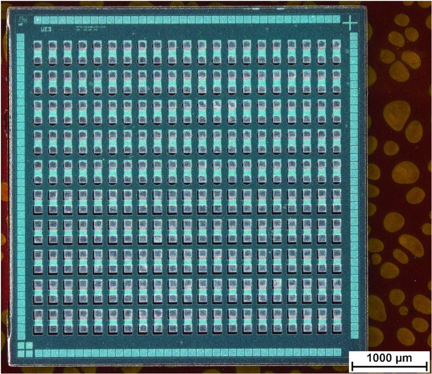
Micromachines 2021, 12, 856                                                                                                 2 of 16

                                    available for electrical connection. Either the chip contact pads are contacted directly by
                                    forming conductive tracks on the chip’s surface or a polymer layer is applied. The choice
                                    of adhesives for the bonding process depends on the substrate material but also on the
                                    used polymer layer and its curing temperature. Often, polyimide is used as a polymer
                                    layer due to its superior thermal, chemical and mechanical stability and its excellent
                                    mechanical flexibility after curing. On the other side, the curing of polyimide requires
                                    an oxygen-free atmosphere and high temperature up to 350 ◦ C for complete curing [11].
                                    Often, benzocyclobutene (BCB) is utilized as an adhesive due to its high thermal stability
                                    and strong adhesion to silicon [12]. Polyimide, as well as BCB, can be applied by spin
                                    coating, resulting in thin layers with homogenous thicknesses [13–15]. Openings in the
                                    polymeric layer can be established by laser drilling [10,16–19] or photolithography [20–22].
                                    Afterwards, conductive tracks are applied. Possible processes for track formation are
                                    printing of inks filled with metal nanoparticles [23,24] or physical vapor deposition (PVD)
                                    of metal layers [13,25–27] in combination with photolithography processes for structuring.
                                          Despite of the apparent advantages of SiF for a broad range of applications and various
                                    known methods for the embedding of ultrathin chips and their electrical contacting, the
                                    breakthrough for products utilizing ultrathin chips has not happened yet. The most likely
                                    reasons are the high manufacturing costs of SiF, especially in the case of prototypes and
                                    its small quantities. This publication presents results from ongoing research on a novel
                                    approach for the coating of face-up bonded chips. This process utilizes conformal spray
                                    coating of a mechanically flexible solder mask resist for embedding adhesively fixed chips
                                    on foil substrates. Solder mask resist is cheaper than polyimide, has excellent adhesion
                                    to silicon and the curing can be performed at 150 ◦ C, which is significantly lower than
                                    the required 350 ◦ C of polyimide. Furthermore, the curing of solder mask resist can be
                                    performed in air atmosphere, in contrast to the oxygen-free atmosphere required for the
                                    imidization process of polyimide. The solder mask resist is structured by a UV direct light
                                    photolithography process to open via to the chip contact pads. Electrically conductive
                                    tracks are printed directly onto the substrate by inkjet printing of nanoparticular silver ink
                                    or nanoparticular gold ink to electrically connect the opened contact pads. The transition
                                    resistances are measured and the achieved values are compared for both inks as well as for
                                    different opening dimensions, opening shapes and printed layer numbers.

                                     2. Materials and Methods
                                         A process flow chart of the proposed fabrication process is shown in Figure 1. In the
                                    beginning, ultrathin chips were bonded face-up onto polyimide foil. Afterwards, the chip
                                    was covered in solder mask resist using conformal coating. Solder mask resist was locally
                                    removed in the area of the chip contact pads by photolithographic processes and cured.
                                    The chip contact pads were electrically connected and conductive tracks were formed by
 Micromachines 2021, 12, 856                                                                                               3 of 17
                                    inkjet printing of silver and gold ink. Each element of the proposed process is explained in
                                    detail in the following subsection.

                                                  Conformal               Photolithographic                 Electrical
                 Adhesive bonding
                                               coating of solder             opening of                   contacting by
                  of ultrathin chip
                                                 mask resist                contact pads                 inkjet printing

                                Figure1.1.Process
                               Figure      Processflow
                                                   flowchart
                                                        chartofofthe
                                                                  theproposed
                                                                      proposedprocess
                                                                               processfor
                                                                                       forthe
                                                                                           thefabrication
                                                                                               fabricationofofSiF.
                                                                                                               SiF.

                                      2.1. Silicon Chip Design and Substrate Preparation
                                          Silicon chips of 4.7 mm × 4.7 mm size were manufactured, thinned to 50 µm thickness
                                      and supplied ready for the pick and place processes by IMS Chips, Stuttgart, Germany.
                                      The chip layout exhibits 210 resistors, which can be connected in a “daisy chain” series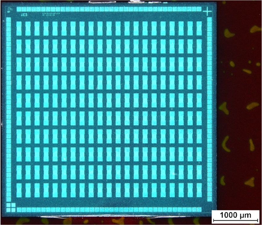
Micromachines 2021, 12, 856                                                                                             3 of 16

                              2.1. Silicon Chip Design and Substrate Preparation
                                   Silicon chips of 4.7 mm × 4.7 mm size were manufactured, thinned to 50 µm thickness
                              and supplied ready for the pick and place processes by IMS Chips, Stuttgart, Germany. The
                              chip layout exhibits 210 resistors, which can be connected in a “daisy chain” series circuit.
                              The ultrathin chips were transferred face-down on a wafer dicing tape (REVALPHA Tape
                              3196, Nitto Denko, Osaka, Japan). An epoxy adhesive (EPO-TEK 354, Epoxy Technology,
                              Billerica, MA, USA) was manually dispensed onto the backside of the chip. A total of
                              75 µm polyimide foil (Flexiso PI FI 16000, Dr. Dietrich Müller GmbH, Ahlhorn, Germany),
                              temporarily fixed on a stiff handling substrate, was placed onto the stack of wafer dicing
                              tape, ultrathin chip and epoxy adhesive. The epoxy adhesive was cured in an oven at 80 ◦ C
                              for 120 min. The adhesion force of the wafer dicing tape to the silicon chip was strongly
                              reduced when exposed to 80 ◦ C for the time of adhesive curing and the wafer dicing tape
                              was peeled off by hand. The surface of the ultrathin chips was cleaned with acetone and
                              cleanroom tissue.

                              2.2. Conformal Coating of Solder Resist
                                    The negative-tone solder mask resist (NPR-80/ID100, Nippon Polytech Corp, Tokyo,
                              Japan) used in this work was manufactured for screen printing as a two component system
                              with a mixing ratio of 100 g resin to 38 g corresponding hardener PF-10/ID36. Both
                              components were weighted according to the recommended mixing ratio and stirred for
                              five minutes. To achieve a lower viscosity suitable for conformal coating, the mixture
                              was diluted 1:1.25 wt% with the solvent propylene glycol methyl ether acetate (PGMEA).
                              The dilution was mixed for five minutes and poured into a 30 mL cartridge sealed with a
                              plunger. The cartridge, together with a barrel adapter, was installed in a conformal coating
                              machine (ELITE DR-070, Nordson DIMA BV, Deurne, The Netherlands). A narrow beam
                              spray coating valve (Type DD-5140, Nordson DIMA BV, Deurne, The Netherlands) was
                              used to achieve a layer thickness of 15–20 µm as recommended in the technical data sheet
                              of the solder mask resist. Empirical trials showed that a dilution ratio of 1:1.25 wt% (NPR-
                              80/ID100: PGMEA) yielded the best tradeoff between application pressure and mixture
                              stability. Lower amounts of PGMEA obtained the high application pressure necessary with
                              the difficulty to obtain the targeted thickness range. Higher amounts of PGMEA led to
                              faster separation of solder mask resist and PGMEA inside the cartridge. In the case of
                              separation, the cartridge can be removed, shaken for five minutes, and re-installed.
                                    During the application process, the valve was moved in multiple parallel tracks in a
                              distance of 20 mm above the substrate with a distance of 15 mm between each track. The
                              application pressure on the plunger was adjusted to 1.5 bar. The atomizer pressure, necessary
                              for the generation of an aerosol for the spray coating process, was set to 0.5 bar. The movement
                              velocity of the valve was set to 450 mm/s. The substrates were laid onto a substrate table heated
                              to 50 ◦ C. The coated substrates stayed for five minutes on the heated table for evaporation of
                              solvent. The substrate was transferred onto an 80 ◦ C hotplate for additional ten minutes for the
                              evaporation of the remaining solvent. Table 1 summarizes the parameters for the conformal
                              spray coating process to achieve a layer thickness of ca. 15 µm.

                              2.3. Exposure and Development
                                   The coated substrates with embedded ultrathin chips were exposed to UV light using
                              a direct light imager system (DI 2020L, MIVA Technologies, Schönaich, Germany) to open
                              the metallic surface of the chip contact pads. The imaging system did not require a physical
                              mask for the UV exposure process. A machine head with built-in UV-LEDs was moved
                              above the vacuum-fixed substrate. Four different wavelengths, namely 365 nm, 375 nm,
                              385 nm and 405 nm, could be used simultaneously as well as individually for the exposure
                              process. For the exposure of the solder mask resist, all wavelengths were used in equal dose
                              proportions. The exposure dose was adjusted by movement velocity of the head as well as
                              the LED current for each wavelength. For the exposure of the coated substrates, the head
                              movement velocity and the LED currents were set to parameters that equaled an exposure
Micromachines 2021, 12, 856                                                                                                4 of 16

                               dose of 1130 mJ/cm2 . Two layouts for the exposure were designed with different via sizes
                               and geometries using conventional PCB layout software. Each layout was divided into
                               circular contact pad openings in the chips upper half and rectangular contact pad openings
                               in the chips lower half. One layout generated circular via openings of 90 µm diameter
                               and rectangular via openings of 90 µm × 90 µm. The other layout generates circular via
                               openings of 130 µm diameter and rectangular via openings of 130 µm × 130 µm. The
                               size of 90 µm was chosen to stay above the stated technical resolvable limit of 80 µm for
                               photolithographic opening size as stated by the manufacturer of the solder mask resist [28].
                               The size of 130 µm was chosen arbitrarily to test ink behavior during and after printing
                               with larger via openings. Areas for exposure as well as virtual markers in two opposite chip
                               corners (Figure 2) are defined within the layouts. The markers served as fiducial points for
                               optical recognition before each UV exposure to ensure alignment. The exposed negative-
                               tone resist was allowed to cross-link for five minutes after UV exposure. The development
                               process was executed for a duration of 30 s in a spray developer using aqueous potassium
                               carbonate solution at 30 ◦ C. The substrate was cleaned afterwards using deionized water.
                               The photolithographic process was completed by thermal curing in an oven at 150 ◦ C for
                               60 min. The summarized exposure, development and thermal curing parameters are listed
                               in Table 2.

                               Table 1. Conformal coating parameters.

                                                       Parameter                                           Value
                                        Mixing ratio solder mask resist: PGMEA                          1:1.25 wt%
                                             Valve distance over substrate                                20 mm
                                                     Track distance                                       15 mm
                                            Cartridge application pressure                                1.5 bar
                                                   Atomizer pressure                                      0.5 bar
                                               Valve movement velocity                                  450 mm/s
                                              Substrate table temperature                                  50 ◦ C
                                       Dwell time after coating on substrate table                         5 min
 Micromachines 2021, 12, 856
                                                 Hotplate temperature                                      80 ◦ C          5 of 17
                                                Dwell time on hotplate                                    10 min

                                Figure2.2. Representation
                               Figure      Representation of
                                                          of virtual
                                                              virtual marker
                                                                      marker in
                                                                              inopposite
                                                                                 oppositechip
                                                                                          chipcorners
                                                                                               cornersfor
                                                                                                       forlayout
                                                                                                           layoutalignment
                                                                                                                  alignmentduring
                                                                                                                            during
                                direct light imaging UV exposure of solder mask resist.
                               direct light imaging UV exposure of solder mask resist.

                               Table 2. Exposure and development parameters.

                                                Parameter                                            Value
                                         LED current value (0–255)                                120 (no unit)
                                           Velocity (100–8000)                                    100 (no unit)
                                              Exposure dose                                       1130 mJ/cm2
                                               Dwell time                                            5 min
Micromachines 2021, 12, 856 5 of 16
Table 2. Exposure and development parameters.
Parameter Value
LED current value (0–255) 120 (no unit)
Velocity (100–8000) 100 (no unit)
Exposure dose 1130 mJ/cm2
Dwell time 5 min
Developer K2 CO3 (0.8% aqueous solution)
Development time 30 s
Development temperature 30 ◦ C
Thermal curing duration 60 min
Thermal curing temperature 150 ◦ C
2.4. Application of Conductive Tracks by Inkjet Printing
Inkjet printing of commercial nanoparticular inks was utilized for electrical contacting
of the chip contact pads. A silver ink (Sicrys I30EG-1, PV Nano Cell, Migdal Ha’Emek,
Israel) as well as a gold ink (DryCure Au-J, C-INK, Soja City, Japan) were printed using a
lab inkjet printer (Dimatix DMP 2850, FUJIFILM Dimatix, Santa Clara, CA, USA) for via
filling and track formation. An amount of 2 mL of ink was filled into cartridges (DMC
11610, Fujifilm, Japan). A filter with 450 nm pore size was used for the silver ink to filter
out agglomerates. The gold ink was filled into the cartridge without filtering. A 10 pL
print head module with 16 nozzles was mounted onto each cartridge and the cartridges
were installed into the printer. A layout for printing was designed using a conventional
PCB layout software. The layout was exported in a monochrome bitmap file with 1016 dpi
resolution. This resolution equals a drop spacing of 25 µm at a cartridge angle of 5.6◦ .
The surface of the substrate was cleaned with acetone and a cleanroom tissue. For the
printing process of both inks, the print head was heated to 35 ◦ C and the temperature of
the substrate table was set to 50 ◦ C. Only one nozzle of 16 potential nozzles was used to
perform the print to allow for fast visible control if the printing nozzle clogs or the ejected
droplets are not shot perpendicular to the surface. The same layout for track printing and
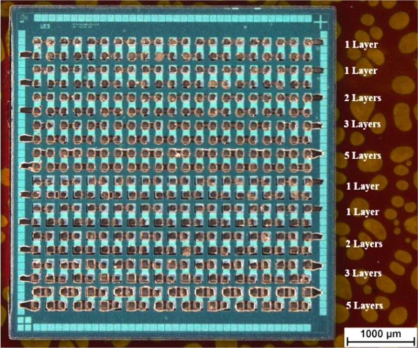
via filling was used for the rectangular and the circular via openings. The number of layers
was varied between the daisy chain structure lines. In total, ten daisy chain lines were
available for printing. The first daisy chain line and the sixth daisy chain line were printed
as a single ink layer to check for correct alignment. For later electrical measurements
the other daisy chain lines were printed as a single ink layer, two ink layers, three ink
layers and five ink layers. This was set as printing strategy for the circular as well as for
the rectangular via openings. An overview over the printed layer count is displayed in
Figure 3. After the printing process, the solvent was mostly evaporated due to the heated
substrate table. The printed nanoparticles were sintered in an oven for 60 min at 150◦ .
The electrical characterization was performed by needle probing in a two-probe electrical
measurement (Multimeter 2002, Keithley Instruments, Cleveland, OH, USA) to determine
the transition resistance. Additionally, white light interferometry (Wyko NT 9100, Bruker,
Billerica, MA, USA) was performed to determine the thickness distribution of printed
tracks. Finally, the foil with the embedded chip was removed from the temporary carrier.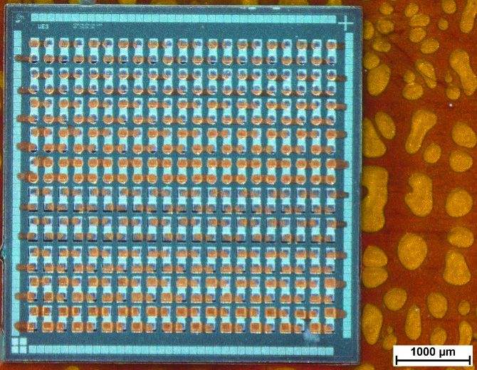
After the printing process, the solvent was mostly evaporated due to the heated substrate
                                     table. The printed nanoparticles were sintered in an oven for 60 min at 150°. The electrical
                                     characterization was performed by needle probing in a two-probe electrical measurement
                                     (Multimeter 2002, Keithley Instruments, Cleveland, OH, USA) to determine the transition
Micromachines 2021, 12, 856          resistance. Additionally, white light interferometry (Wyko NT 9100, Bruker, Billerica, MA,
                                                                                                                              6 of 16
                                     USA) was performed to determine the thickness distribution of printed tracks. Finally, the
                                     foil with the embedded chip was removed from the temporary carrier.

                                     Figure 3. Overview of printed layers for each daisy chain line. First and sixth line were printed for
                                    Figure 3. Overview of printed layers for each daisy chain line. First and sixth line were printed for
                                     alignment with one layer each. The other lines were printed for electrical measurement with varying
                                    alignment
                                     number ofwith   one layer each. The other lines were printed for electrical measurement with varying
                                                layers.
                                    number of layers.
                                     3. Results
                                    3. Results
                                          The wafer dicing tape can be removed easily without damages to the silicon chips.
                                          The wafer dicing tape can be removed easily without damages to the silicon chips.
                                     Remaining adhesive from the wafer dicing tape on the surface of the epoxy bonded chips
                                    Remaining adhesive from the wafer dicing tape on the surface of the epoxy bonded chips
                                     was mechanically cleaned using acetone and clean room tissues. A chip on polyimide foil
                                    was mechanically cleaned using acetone and clean room tissues. A chip on polyimide
                                     after acetone cleaning is displayed in Figure 4. Further details about the ultrathin chip
                                    foil after acetone cleaning is displayed in Figure 4. Further details about the ultrathin
                                     bonding process using a wafer dicing tape as a temporary chip carrier can be found in
                                    chip bonding process using a wafer dicing tape as a temporary chip carrier can be found
                                     [29,30]. After cleaning, a layer of solder mask resist was spray coated onto the ultrathin
                                    in [29,30]. After cleaning, a layer of solder mask resist was spray coated onto the ultrathin
                                     chip. Figure 5 shows the surface of an ultrathin chip embedded in spray coated solder
  Micromachines 2021, 12, 856       chip. Figure 5 shows the surface of an ultrathin chip embedded in spray coated          solder
                                                                                                                         7 of 17
                                     mask resist.
                                    mask resist.

                                    (a)                                                                   (b)
        Figure
      Figure 4. 4.
                (a)(a)Ultrathin
                       Ultrathinchip
                                 chipepoxy
                                      epoxybonded
                                             bonded on
                                                     on polyimide
                                                         polyimide foil.
                                                                     foil. Remaining
                                                                           Remainingadhesive
                                                                                     adhesivefrom
                                                                                               fromwafer
                                                                                                     waferdicing tape
                                                                                                            dicing tapeis is
                                                                                                                          visible onon
                                                                                                                             visible thethe
        surface after  removing   the wafer dicing tape. (b) Surface  of epoxy bonded ultrathin chip after acetone cleaning.
      surface after removing the wafer dicing tape. (b) Surface of epoxy bonded ultrathin chip after acetone cleaning.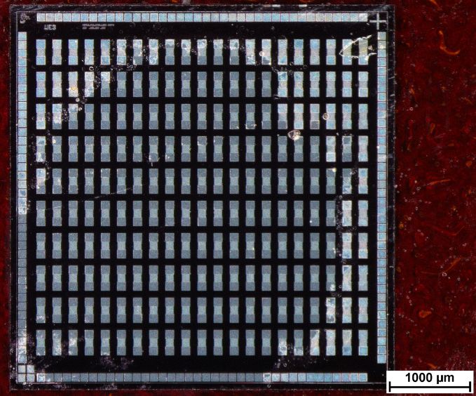
(a)                                                                 (b)
  Micromachines 2021, 12, 856                                                                                                       7 of 16
         Figure 4. (a) Ultrathin chip epoxy bonded on polyimide foil. Remaining adhesive from wafer dicing tape is visible on the
         surface after removing the wafer dicing tape. (b) Surface of epoxy bonded ultrathin chip after acetone cleaning.

                                     Figure 5.5. Ultrathin
                                     Figure      Ultrathin chip
                                                            chipwith
                                                                withdaisy
                                                                     daisychain
                                                                           chainstructures
                                                                                 structuresembedded
                                                                                            embeddedin  insolder
                                                                                                           soldermask
                                                                                                                  maskresist.
                                                                                                                        resist.The
                                                                                                                                Thebubbles
                                                                                                                                    bubbles
                                     visible in the background right from the chip are located in an adhesive layer. This adhesive layer
                                     visible in the background right from the chip are located in an adhesive layer. This adhesive layer is
                                     is used as temporary fixation of a polyimide foil on a stiff handling substrate.
                                     used as temporary fixation of a polyimide foil on a stiff handling substrate.

                                           The different
                                           The  different via
                                                           viaopenings
                                                               openingsafter photolithography
                                                                         after  photolithographyare are
                                                                                                    shown   in Figures
                                                                                                         shown         6 and 67. and
                                                                                                                 in Figures      Figure
                                                                                                                                      7.
                                      6 shows  circular via openings of 90  µm  diameter  and 130  µm  diameter,  respectively.
                                     Figure 6 shows circular via openings of 90 µm diameter and 130 µm diameter, respectively.   Figure
                                      7 shows7 rectangular
                                     Figure                  via openings
                                                shows rectangular          of 90 µmof× 90
                                                                     via openings       90 µm
                                                                                           µm and
                                                                                                × 90 130
                                                                                                       µmµmand× 130
                                                                                                                 130µm,
                                                                                                                     µmrespectively.
                                                                                                                           × 130 µm,
Micromachines 2021, 12, 856           Figure 8 shows   an overview  of an  embedded   chip  with  circular via openings
                                     respectively. Figure 8 shows an overview of an embedded chip with circular via      in openings
                                                                                                                            the upper
                                                                                                                                    8 of 17
                                      half and rectangular   via openings  in the lower  half with 130  µm  feature sizes.
                                     in the upper half and rectangular via openings in the lower half with 130 µm feature sizes.

                                  (a)                                                                     (b)
                       Figure
                         Figure6.6.Circular
                                    Circularvia
                                             viaopenings
                                                 openings with (a) aa diameter
                                                          with (a)    diameterofof90
                                                                                   90µm
                                                                                      µmand
                                                                                         and(b)(b) a diameter
                                                                                                 a diameter of of
                                                                                                               130130
                                                                                                                   µm.µm.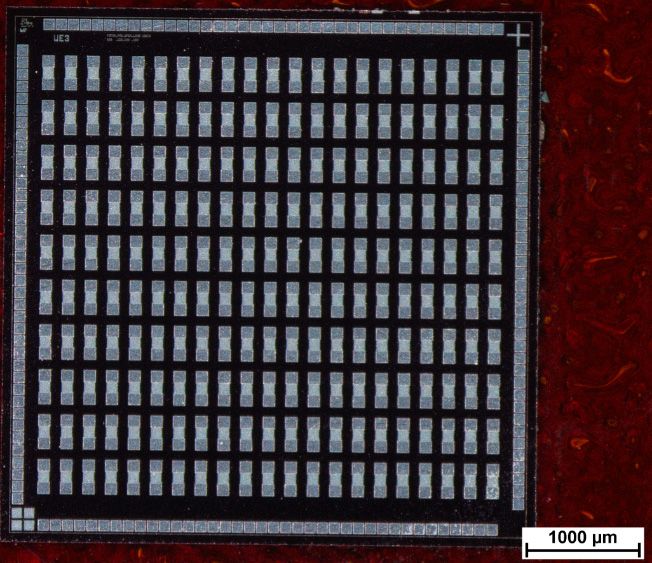
Micromachines 2021, 12, 856                                                                                                          8 of 16
                              (a)                                                              (b)
                                 (a)                                                               (b)
                  Figure 6. Circular via openings with (a) a diameter of 90 µm and (b) a diameter of 130 µm.
                      Figure 6. Circular via openings with (a) a diameter of 90 µm and (b) a diameter of 130 µm.

                              (a)                                                               (b)
                                  (a)                                                                (b)
                       Figure
                          Figure 7. Rectangular via openings (a) 90 µm × 90 µm and (b) 130 µm × 130 µm.µm.
                              7. Rectangular  via  openings of (a) 90 µm × 90 µm and (b) 130 µm  × 130
                           Figure 7. Rectangular via openings of (a) 90 µm × 90 µm and (b) 130 µm × 130 µm.

                               Figure 8. Overall view on an ultrathin chip embedded in solder mask after photolithographic struc-
                                   Figure8.8.Overall
                                               Overall viewon onan
                                                                 anultrathin
                                                                    ultrathinchip
                                                                                chipembedded
                                                                                      embedded in in solder   mask after    photolithographic struc
                               turing. The opening view
                                  Figure              dimensions    are 130 µm. The      bubbles   solder
                                                                                                   visible mask
                                                                                                           in theafter   photolithographic
                                                                                                                    background    are located in
                                   turing. The   opening
                                  structuring.layer.
                                                The openingdimensions
                                                             dimensions  are  130
                                                                         areis130   µm.  The
                                                                                       The   bubbles   visible
                                                                                           bubbles visible       in
                                                                                                            in the  the  background     are located i
                               an adhesive           This adhesive   layer     usedµm.as temporary    fixation   ofbackground
                                                                                                                    a polyimide arefoil
                                                                                                                                    located
                                                                                                                                         on a stiff
                                   an  adhesive
                                  in an adhesive  layer.  This adhesive   layer   is used as temporary     fixation   of  a polyimide
                                                  layer. This adhesive layer is used as temporary fixation of a polyimide foil on a stifffoil on a sti
                               handling  substrate.
                                   handlingsubstrate.
                                  handling     substrate.

                                         Figure 9 shows an overview over embedded ultrathin chips with 130 µm via opening
                                    sizes after silver ink and gold ink inkjet printing. Figure 10 demonstrates the difference
                                    between one printed silver layer and five printed silver layers for 130 µm × 130 µm
                                    rectangular via openings after sintering the silver ink. Figure 11 demonstrates the difference
                                    between one printed gold layer and five printed gold layers for 90 µm circular via openings
                                    after sintering the gold ink.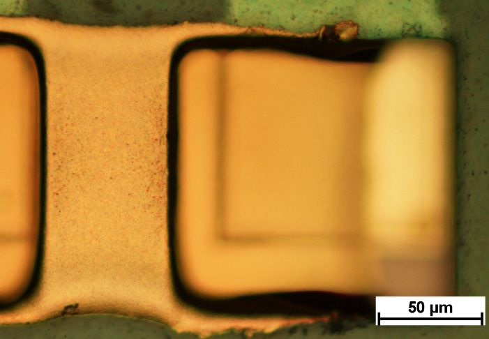
Figure 9 shows an overview over embedded ultrathin chips with 130 µm via opening
sizes Figure 9 shows
after silver inkan
andoverview
gold inkover embedded
inkjet printing.ultrathin
Figure 10chips with 130 µm
demonstrates thevia opening
difference
sizes afterone
between silver ink and
printed gold
silver inkand
layer inkjet
fiveprinting. Figurelayers
printed silver 10 demonstrates
for 130 µm the
× 130difference
µm rec-
Micromachines 2021, 12, 856 between one printed silver layer and five printed silver layers for 130 µm × 130 µm rec-
tangular via openings after sintering the silver ink. Figure 11 demonstrates the difference 9 of 16
tangular via openings after sintering the silver ink. Figure 11 demonstrates the
between one printed gold layer and five printed gold layers for 90 µm circular via open-difference
between
ings afterone printed
sintering thegold
goldlayer
ink. and five printed gold layers for 90 µm circular via open-
ings after sintering the gold ink.
(a) (b)
(a) (b)
Figure
Figure 9. 9. Overall
Overall viewafter
view afterprinting
printingand
andsintering
sinteringof
of (a)
(a) silver
silver ink
ink and
and (b)
(b) gold
goldink.
ink.The
Thenotation
notationdisplays
displaysthe numbers
the of of
numbers
Figure 9.layers
printed Overall
for view
each after printing
daisy chain and sintering of (a) silver ink and (b) gold ink. The notation displays the numbers of
line.
printed layers for each daisy chain line.
printed layers for each daisy chain line.
(a) (b)
(a) (b)
Figure 10. Connection between rectangular via openings of 130 µm × 130 µm size. (a) One layer of printed silver ink after
Figure
10.10.
sintering.
Figure
Micromachines Connection
(b)
2021,Five
Connection between
layers
12, 856 rectangular
of printed
between via
silver ink
rectangular via openings
after of130
sintering.
openings of 130µm
µm ×
× 130
130 µm
µmsize.
size.(a)
(a)One
Onelayer
layerofofprinted
printedsilver ink
silver after
ink after10 of 17
sintering. (b) Five layers of printed silver ink after sintering.
sintering. (b) Five layers of printed silver ink after sintering.
(a) (b)
Figure
Figure 11. Connection
11. Connection between
between circular
circular viavia openings
openings of of
90 90
µmµm diameter.
diameter. (a)(a)
OneOne layer
layer ofof printedgold
printed goldink
inkafter
aftersintering.
sintering.
(b) Five layers of printed gold ink after sintering.
(b) Five layers of printed gold ink after sintering.
The layer structure, presented in Figure 12, shows the three factors that influence the
transition resistance from one probe needle to the other probe needle. The first factor is
the resistance of the ink itself. The second factor is the contact resistance at the interface
ink to contact pad. The third factor is the resistance of the buried resistor. The nominal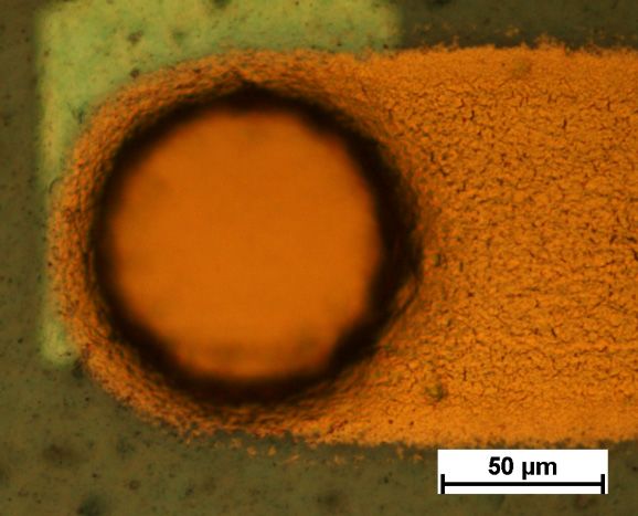
(a) (b)
Micromachines 2021, 12, 856 10 of 16
Figure 11. Connection between circular via openings of 90 µm diameter. (a) One layer of printed gold ink after sintering.
(b) Five layers of printed gold ink after sintering.
The
The layer
layer structure,
structure, presented
presented in in Figure
Figure12, 12, shows
shows the the three
three factors
factorsthat
that influence
influencethe the
transition
transitionresistance
resistancefromfromoneoneprobe
probe needle
needleto tothethe
other
otherprobe needle.
probe TheThe
needle. firstfirst
factor is theis
factor
resistance
the resistanceof theofink
theitself. The second
ink itself. The secondfactorfactor
is the is
contact resistance
the contact at the interface
resistance ink to
at the interface
contact pad. The third factor is the resistance of the buried resistor.
ink to contact pad. The third factor is the resistance of the buried resistor. The nominal The nominal value of
resistance of the buried resistor is 1 Ω. The mean resistance values
value of resistance of the buried resistor is 1 Ω. The mean resistance values and standard and standard deviation
of the measured
deviation transitiontransition
of the measured resistances for rectangular
resistances and circular
for rectangular via openings
and circular with
via openings
varying sizes and
with varying sizesdifferent layer count
and different layer are
countsummarized
are summarized in Tablein3Table
for the3 silver
for theink andink
silver in
Table 4 for the gold ink. Each entry shows the mean resistance value
and in Table 4 for the gold ink. Each entry shows the mean resistance value and standard and standard deviation
for a daisyfor
deviation chain linechain
a daisy with line
21 transitions. It is noted
with 21 transitions. It isifnoted
a transition was not
if a transition wasmeasurable
not meas-
due to a defect by an interruption in the printed track. In this
urable due to a defect by an interruption in the printed track. In this case, the mean case, the mean values and
values
standard deviation values were calculated from the remaining
and standard deviation values were calculated from the remaining transition structures.transition structures.
Figure 12.
Figure 12. Schematic
Schematic layer
layer structure
structure (not
(not to
to scale)
scale) of
ofan
anepoxy
epoxybonded
bondedchipchipon
onpolyimide
polyimidesubstrate
substrate
and embedded
and embedded in in solder
solder mask.
mask. The
The chip
chip exhibits
exhibits buried
buried resistors
resistors (1
(1 Ω).
Ω). The
The contacts
contacts pads
pads of
of the
the
buried resistors were opened and contacted by inkjet printing. Mainly three factors
buried resistors were opened and contacted by inkjet printing. Mainly three factors influence the influence the
transition resistance from the first probe needle to the other probe needle. (1) Resistance of the
transition resistance from the first probe needle to the other probe needle. (1) Resistance of the printed
printed track; (2) contact resistance at the interface; (3) the resistance of the buried resistor.
track; (2) contact resistance at the interface; (3) the resistance of the buried resistor.
Table 3. Results of electrical characterization of transition resistances of printed silver tracks.
Table 3. Results of electrical characterization of transition resistances of printed silver tracks.
Transition Resistances Number of Layers
Transition Resistances Ink: Silver Ink: Silver 1 LayerNumber2ofLayers
Layers
3 Layers 5 Layers
Circular 1 Layer 2 Layers
211.3 Ω 189.6 Ω3 Layers
47 Ω 5 Layers
51.1 Ω
90 µm
211.3 Ω ± 121.1 Ω Ω ± 299
90 µm openings 189.6
± 121.1 ΩΩ Ω ± 36.1 Ω± 36.1 Ω 51.1 Ω ±
47 Ω
± 299 30.4ΩΩ
± 30.4
Circular openings 19 defects: 2 defects:
130 µm 2.2 kΩ ± 5.8 Ω 129 Ω ± 109.6 Ω
11 MΩ ± 1.4 MΩ 33.4 MΩ ± 124.1 MΩ
90 × 90 µm2 64.3 Ω ± 19.2 Ω 44.5 Ω ± 24 Ω 69.6 Ω ± 87.7 Ω 36.4 Ω ± 21.4 Ω
Rectangular
openings 14 defects: 4 defects:
130 × 130 µm2 399.5 kΩ ± 1.7 MΩ 28.9 kΩ ± 129.7 kΩ
6.2 MΩ ± 8.7 MΩ 1.8 MΩ ± 3.8 MΩ
Table 4. Results of electrical characterization of transition resistances of printed gold tracks.
Number of Layers
Transition Resistances Ink: Gold
1 Layer 2 Layers 3 Layers 5 Layers
90 µm 33.4 kΩ ± 152.7 kΩ 18.8 Ω ± 5.9 Ω 15.6 Ω ± 9.5 Ω 12.9 Ω ± 7 Ω
Circular openings 1 defect:
130 µm 16.7 Ω ± 6 Ω 11.9 Ω ± 3 Ω 9.9 Ω ± 3.7 Ω
1.2 MΩ ± 2.3 MΩ
90 × 90 µm2 287.2 kΩ ± 591 kΩ 16.7 Ω ± 6.3 Ω 14 Ω ± 8.9 Ω 14 Ω ± 11.2 Ω
Rectangular
openings 3 defects:
130 × 130 µm2 14.9 Ω ± 3.9 Ω 9.6 Ω ± 2.6 Ω 9.6 Ω ± 9.6 Ω
5.8 MΩ ± 8.8 MΩ± 2.3 MΩ
287.2 kΩ 16.7 Ω 14 Ω 14 Ω
90 × 90 µm2
± 591 kΩ ± 6.3 Ω ± 8.9 Ω ± 11.2 Ω
Rectangular
3 defects:
openings 14.9 Ω 9.6 Ω 9.6 Ω
Micromachines 2021, 12, 856 130 × 130 µm2 5.8 MΩ 11 of 16
± 3.9 Ω ± 2.6 Ω ± 9.6 Ω
± 8.8 MΩ
White light interferometry measurement results showed higher thicknesses for the
silver White
tracks light interferometry
(Figure 13 for 90 µmmeasurement
diameter andresults
Figureshowed higher
14 for 130 thicknesses
µm diameter) for for
than the
silver tracks (Figure 13 for 90 µm diameter and Figure 14 for 130 µm diameter)
the gold tracks (Figure 15 for 90 µm diameter and Figure 16 for 130 µm diameter). Fur- than for the
gold tracks (Figure 15 for 90 µm diameter and Figure 16 for 130 µm diameter). Furthermore,
thermore, silver nanoparticles rather gather in the peripheral region in contrast to gold
silver nanoparticles
nanoparticles rather gather
that concentrate in the
in the peripheral
center region in contrast to gold nanoparticles
of the track.
that concentrate in the center of the track.
Sicrys I30EG1, 90 µm circular openings
3.5
3
2.5
2
Height (µm)
1.5 1 Layer
3 Layers
1
5 Layers
0.5
0
-0.5
0 20 40 60 80 100 120 140 160 180
Measurement distance (µm)
Micromachines 2021, 12, 856 12 of 17
Figure 13. White light interferometry measurement of the silver track thickness between circular via openings with 90 µm
Figure 13. after
diameter White1,light
3 andinterferometry measurement of the silver track thickness between circular via openings with 90 µm
5 printed layers.
diameter after 1, 3 and 5 printed layers.
Sicrys I30EG1, 130 µm circular openings
3.5
3
2.5
2
Height (µm)
1.5 1 Layer
3 Layers
1
5 Layers
0.5
0
-0.5
0 10 20 30 40 50 60 70 80 90
Measurement distance (µm)
Figure 14. White light interferometry measurement of the silver track thickness between circular via openings with 130 µm
Figure 14. after
diameter White1, light
3 andinterferometry measurement of the silver track thickness between circular via openings with 130
5 printed layers.
µm diameter after 1, 3 and 5 printed layers.
DryCure AuJ, 90 µm circular openings
1-0.5
0 10 20 30 40 50 60 70 80 90
Measurement distance (µm)
Micromachines 2021, 12, 856 12 of 16
Figure 14. White light interferometry measurement of the silver track thickness between circular via openings with 130
µm diameter after 1, 3 and 5 printed layers.
DryCure AuJ, 90 µm circular openings
1
0.75
0.5
Height (µm)
0.25 1 Layer
3 Layers
0 5 Layers
-0.25
-0.5
0 50 100 150 200 250
Measurement distance (µm)
Micromachines 2021, 12, 856 13 of 17
Figure 15. White light interferometry measurement of the gold track thickness between circular via openings with 90 µm
Figure 15. after
diameter White 1, light
3 andinterferometry measurement of the gold track thickness between circular via openings with 90 µm
5 printed layers.
diameter after 1, 3 and 5 printed layers.
DryCure AuJ, 130 µm circular openings
1
0.75
0.5
Height (µm)
0.25 1 Layer
3 Layers
0 5 Layers
-0.25
-0.5
0 20 40 60 80 100 120 140 160 180 200
Measurement distance (µm)
Figure 16. White light interferometry measurement of the gold track thickness between circular via openings with 130 µm
Figure 16. after
diameter White 1, light
3 andinterferometry measurement of the gold track thickness between circular via openings with 130 µm
5 printed layers.
diameter after 1, 3 and 5 printed layers.
The removal of the foil with the embedded chip from the temporary carrier was
The removal
performed of the foil
by peeling with17).
(Figure the embedded
The solderchip
maskfrom
as the temporary
well carrier was
as the ultrathin chipper-
are
formed by peeling
mechanically (Figure 17). The solder mask as well as the ultrathin chip are mechani-
flexible.
cally flexible.Figure 16. White light interferometry measurement of the gold track thickness between circular via openings with 130 µm
diameter after 1, 3 and 5 printed layers.
Micromachines 2021, 12, 856 The removal of the foil with the embedded chip from the temporary carrier was 13per-
of 16
formed by peeling (Figure 17). The solder mask as well as the ultrathin chip are mechani-
cally flexible.
(a) (b)
Figure
Figure17.
17.(a)(a)Removing
Removingofofpolyimide
polyimidefoil
foilsubstrate
substratebybypeeling
peelingoff
offofofthe
thetemporary
temporarycarrier
carriersubstrate.
substrate.(b)
(b)Mechanically
Mechanically
flexible ultrathin chip embedded in solder mask resist.
flexible ultrathin chip embedded in solder mask resist.
4.4.
Discussion
Discussion
The
Themanufacturer
manufacturerofofthethesolder
soldermask
maskresist
resist intended applicationby
intended the application byscreen
screenprinting.
print-
ing.
To To avoid
avoid thethe needfor
need fora ascreen,
screen,the
the solder
solder mask resist application
applicationwaswastransferred
transferredtoto
a conformal
a conformal coating machine.
coating machine. For aFor
more versatile
a more spray spray
versatile coating process,
coating the solder
process, the mask
solder
resist
mask mixture was diluted
resist mixture using PGMEA,
was diluted a standard
using PGMEA, solventsolvent
a standard in photolithography tech-
in photolithography
nology. A combination
technology. of a mixing
A combination ratio, ratio,
of a mixing application pressure
application and valve
pressure movement
and valve ve-
movement
velocity
locity generated
generated a homogeneous
a homogeneous layer
layer without
without defects.
defects. TheThe thickness
thickness of of
thethe solder
solder mask
mask
layercan
layer canbebeinfluenced
influencedbybythetheadjustment
adjustmentofofthe thevalve
valvemovement
movementvelocity.
velocity.Conformal
Conformal
coating allows for a locally defined application of resist saving material and reducing
cleaning expenses compared to the full area coverage of spin coating. Further arbitrary
substrate geometries can be coated, while spin coating is limited to round substrates.
For the UV exposure of the photosensitive solder mask resist, a dose of 1130 mJ/cm2
was found to be sufficient to start the cross-linking reactions in the material. The most
influential factor on the resulting resist mask was the development duration. On the one
hand, the duration of the development process must be chosen long enough to remove
all insulating solder mask material on the chip contact pads. On the other hand, the edge
formation of the solder mask was deteriorated if the sprayed developer reacted for too
long with the solder mask. Instead of the recommended 60 s, the development duration
was reduced to 30 s. All contact pad openings were successfully opened after development.
This demonstrated that thinning with PGMEA is possible. In comparison with conventional
mask photolithography, the utilization of direct light imaging offers a significantly faster
development process of new prototypes. The layout can be altered digitally in a short time
without an additional costly fabrication of a new set of masks.
The white light interferometry measurements show a clearly noticeable coffee-stain
effect for the silver ink, where the nanoparticles were affected by a forced flow towards
the peripheral regions of the wetted area due to a gradient of surface tension. In contrast,
the gold particles were concentrated in the center of the printed track due to a Marangoni
flow. Furthermore, the higher content of silver nanoparticles (30 wt%) in the silver ink
Sicrys I30EG-1 compared to gold nanoparticles (10 wt%) within the gold ink DryCure Au-J,
contributed to a higher track thickness of printed silver.
The measurements of transition resistances listed in Tables 3 and 4 show mixed results.
It should be noted that inhomogeneous track thicknesses affected the measured resistance
values during needle probing. A placement of the needles in the peripheral region of the
printed track showed different resistance values than a measurement in the center of the
printed tracks dependent on the printed ink. For silver ink, a smaller opening dimensions
showed lower resistance values and no defects in comparison to larger via openings with
multiple defects. Gold ink did not show this distinct difference. This may result fromMicromachines 2021, 12, 856 14 of 16
a combination of different wetting behaviors of the inks and residual solder mask resist
after development in the 90 µm via openings that served as a ramp for the inks. The silver
ink Sicrys I30EG-1 was based on ethylene glycol as the solvent. The gold nanoparticles
of DryCure Au-J were dispersed in a water–glycerol mixture. The lower surface tension
of ethylene glycol may have caused a disconnection between the ink on the top of the
solder mask resist and the ink in the via opening. The largest proportion of the ink flowed
downwards into the via opening without adhesion to the wall of the via opening. As
a result, the wall coverage was insufficient, resulting in defects and high resistances. A
ramp of residual solder mask can bridge the difference in height and aid the formation of a
conductive track. A higher number of layers cannot completely compensate the poor wall
coverage, but increases the risk of merging of excessive ink. The higher surface tension
of the water–glycerol mixture may prevent disconnection between the ink on top of the
solder mask and ink in the via opening. The influence of surface tension and wettability of
solder mask on wall coverage will be investigated in future work.
Defect-free tracks and connections were achieved by gold ink printing of a minimum
of two layers. Printing of only one layer resulted in very low track thicknesses insufficient
for reliable track formation. The variation between circular and rectangular openings as
well as the influence of additional numbers of layers was marginal. One assumption for
higher standard deviation in resistance values for five printed layers was the increased
risk of micro crack formation with increasing metal thickness due to thermo-mechanical
stresses during sintering. Further analysis, such as thermal shock or humidity reliability
testing, is needed to determine the influencing factors on resistance values and the possible
cause of failures.
5. Conclusions
This publication presented the successful embedding of ultrathin silicon chips on
polyimide foil in mechanically flexible solder mask resist and their electrical contacting
by inkjet printing. The solder mask resist, manufactured for screen printing, was diluted
and spray coated on epoxy bonded ultrathin chips on foil. The solder mask resist was
photolithographically structured by UV-LED direct light exposure and developed to form
openings above the chip contact pads. Opening sizes of 90 µm and 130 µm, as well as
circular and rectangular opening layouts, were applied. For electrical contacting of chip
contact pads, tracks were inkjet printed using commercial inks with silver nanoparticles as
well as gold nanoparticles. Layer counts of one layer, two layers, three layers as well as
five layers were printed with both inks.
The comparison of resistance values showed generally lower resistances and lower
standard deviations for the gold ink DryCure Au-J. Similar to the silver ink Sicrys I30EG-1,
the 90 µm openings showed better results than 130 µm openings probably due to the
residual material in the openings. In general, printing of more than one layer was necessary
to achieve reliable track formation. Printing of five layers of gold ink mostly increased
the standard deviation of resistance compared to three printed layers. Regarding also
the economic aspects, printing of two gold ink layers is the most efficient way. The
presented processes are especially suited for fast development and rapid prototyping of
SiF applications due to the utilization of conformal coating, direct light imaging and inkjet
printing. Photolithographic layouts, as well as inkjet printed track layouts, can be altered
quickly due to direct light imaging as a mask-less digital process. Spray-coated areas, direct
light-exposed areas as well as inkjet-printed tracks originating from a digital layout defined
in a software without additional tools or masks for layout shaping. Thereby, SiF can be
manufactured in various configurations for comparably low costs and short time compared
to existing technologies.
In the future, ultrathin glass as the mechanically flexible substrate could be inves-
tigated as an alternative substrate material, especially for sensor applications in high
temperature environments [31]. The proposed fabrication process was also interesting for
embedding and electrical contacting of ultrathin electronics grown on mechanically flexibleMicromachines 2021, 12, 856 15 of 16
substrates such as thin metals [32], thinned semiconductors [33] or ultrathin ceramics [34],
achieving SiF with very low overall thicknesses suitable for various environments and
sensor applications.
Author Contributions: Funding acquisition, K.G. and A.Z.; Investigation, F.J., N.E. and S.W.; Method-
ology, F.J. and S.W.; Project administration, K.G.; Resources, S.W.; Supervision, W.E. and A.Z.;
Writing—original draft, F.J.; Writing—review and editing, K.G., W.E. and A.Z. All authors have read
and agreed to the published version of the manuscript.
Funding: This research was funded by the Ministry for Economic Affairs, Labour and Tourism
Baden-Württemberg of Baden-Wuerttemberg, Germany, within the project “BW Elektrolyse”.
Institutional Review Board Statement: Not applicable.
Informed Consent Statement: Not applicable.
Acknowledgments: The research presented in this paper is supported from the budget of the
Ministry for Economic Affairs, Labour and Tourism Baden-Württemberg (Project “BW Elektrolyse”).
We would like to thank the funding organization.
Conflicts of Interest: The authors declare no conflict of interest. The funders had no role in the design
of the study; in the collection, analyses, or interpretation of data; in the writing of the manuscript, or
in the decision to publish the results.
References
1. Gupta, S.; Navaraj, W.T.; Lorenzelli, L.; Dahiya, R. Ultra-thin chips for high-performance flexible electronics. NPJ Flex. Electron.
2018, 2. [CrossRef]
2. Burghartz, J.N.; Appel, W.; Rempp, H.D.; Zimmermann, M. A New Fabrication and Assembly Process for Ultrathin Chips. IEEE
Trans. Electron Devices 2009, 56, 321–327. [CrossRef]
3. Lee, J.H.; Lee, C.W.; Kim, Y.J.; Kim, S.M.; Song, J.Y. Development of PEB face-down interconnection process for ultra thin flexible
package. In Proceedings of the 21st European Microelectronics and Packaging Conference (EMPC) & Exhibition, Warsaw, Poland,
10–13 September 2017; pp. 1–4. [CrossRef]
4. van den Brand, J.; Kusters, R.; Heeren, M.; van Remoortere, B.; Dietzel, A. Flipchip bonding of ultrahin Si dies onto PEN/PET
substrates with low cost circuitry. In Proceedings of the 3rd Electronics System Integration Technology Conference (ESTC 2010),
Berlin, Germany, 13–16 September 2010.
5. Haberland, J.; Becker, M.; Lutke-Notarp, D.; Kallmayer, C.; Aschenbrenner, R.; Reichl, H. Ultrathin 3D ACA flipchip-in-flex
technology. In Proceedings of the International Conference and Exhibition on Device Packaging 2010, Held in Conjunction with
the Global Business Council, GBC 2010 Spring Conference, Scottsdale, AZ, USA, 9–10 March 2010; pp. 2154–2161.
6. Lin, Y.M.; Zhan, C.J.; Hsiao, Z.C.; Fu, H.C.; Cheng, R.S.; Huang, Y.W.; Huang, S.Y.; Chen, S.M.; Fan, C.W.; Chien, C.H.; et al.
A novel 3D IC assembly process for ultra-thin chip stacking. In Proceedings of the 2014 International Conference on Electronics
Packaging (ICEP 2014), Toyama, Japan, 23–25 April 2014; pp. 470–474. [CrossRef]
7. Quintero, A.V.; Briand, D.; de Rooij, N.F. Flip-chip integration of Si bare dies on polymeric substrates at low temperature using
ICA vias made in dry film photoresist. J. Micromech. Microeng. 2015, 25, 045013. [CrossRef]
8. Haberland, J.; Pahl, B.; Kallmayer, C.; Aschenbrenner, R.; Reichl, H. Super thin flip chip assemblies on flex substrates-adhesive
bonding and soldering technology-reliability investigations and applications. In Proceedings of the International Symposium on
Microelectronics 2006, San Diego, CA, USA, 8–12 October 2006.
9. Kim, J.H.; Lee, T.I.; Shin, J.W.; Kim, T.S.; Paik, K.W. Ultra-thin chip-in-flex (CIF) technology using anisotropic conductive films
(ACFs) for wearable electronics applications. In Proceedings of the 2015 IEEE 65th Electronic Components and Technology
Conference (ECTC), San Diego, CA, USA, 26–29 May 2015; pp. 714–718. [CrossRef]
10. Klink, G.; Feil, M.; Ansorge, F.; Aschenbrenner, R.; Reichl, H. Innovative packaging concepts for ultra thin integrated circuits. In
Proceedings of the 2001 IEEE 51st Electronic Components and Technology Conference (ECTC), Orlando, FL, USA, 29 May–1 June 2001;
pp. 1034–1039.
11. Govaerts, J.; Christiaens, W.; Bosman, E.; Vanfleteren, J. Fabrication Processes for Embedding Thin Chips in Flat Flexible Substrates.
IEEE Trans. Adv. Packag. 2009, 32, 77–83. [CrossRef]
12. Priyabadini, S.; Sterken, T.; Wang, L.; Dhaenens, K.; Vandecasteele, B.; Van Put, S.; Petersen, A.E.; Vanfleteren, J. An approach to
produce a stack of photo definable polyimide based flat UTCPs. In Proceedings of the 2012 4th Electronic System-Integration
Technology Conference, Amsterdam, The Netherlands, 17–20 September 2012; pp. 1–4. [CrossRef]
13. Alavi, G.; Sailer, H.; Albrecht, B.; Harendt, C.; Burghartz, J.N. Adaptive Layout Technique for Microhybrid Integration of
Chip-Film Patch. IEEE Trans. Compon. Packag. Manuf. Technol. 2018, 8, 802–810. [CrossRef]Micromachines 2021, 12, 856 16 of 16
14. Loher, T.; Seckel, M.; Pahl, B.; Bottcher, L.; Ostmann, A.; Reichl, H. Highly integrated flexible electronic Circuits and Modules. In
Proceedings of the 2008 3rd International Microsystems, Packaging, Assembly & Circuits Technology Conference, Taipei, Taiwan,
22–24 October 2008; pp. 86–89.
15. Hassan, M.; Schomburg, C.; Harendt, C.; Penteker, E.; Burghartz, J.N. Assembly and Embedding of Ultra-Thin Chips in Polymers. In
Proceedings of the 2013 European Microelectronics Packaging Conference (EMPC), Grenoble, France, 9–12 September 2013; pp. 1–6.
16. Manessis, D.; Boettcher, L.; Ostmann, A.; Aschenbrenner, R.; Reichl, H. Chip embedding technology developments leading to the
emergence of miniaturized system-in-packages. In Proceedings of the 18th European Microelectronics & Packaging Conference,
Brighton, UK, 12–15 September 2010; pp. 803–810. [CrossRef]
17. Zoschke, K.; Mackowiak, P.; Ngo, H.D.; Tschoban, C.; Fritsche, C.; Kröhnert, K.; Fischer, T.; Ndip, I.; Lang, K.D. High-density flexible
substrate technology with thin chip embedding and partial carrier release option for IoT and sensor applications. In Proceedings of
the 2019 IEEE 69th Electronic Components and Technology Conference (ECTC), Las Vegas, NV, USA, 28–31 May 2019; pp. 1475–1484.
[CrossRef]
18. Christiaens, W.; Loeher, T.; Pahl, B.; Feil, M.; Vandevelde, B.; Vanfleteren, J. Embedding and assembly of ultrathin chips in
multilayer flex boards. Circuit World 2008, 34, 3–8. [CrossRef]
19. Kugler, A.; Koyuncu, M.; Zimmermann, A.; Kostelnik, J. Chip Embedding in Laminates. In Ultra-Thin Chip Technology and
Applications; Burghartz, J., Ed.; Springer: New York, NY, USA, 2011; pp. 159–165.
20. Ostmann, A.; Neumann, A.; Weser, S.; Jung, E.; Böttcher, L.; Reichl, H. Realization of a stackable package using chip in polymer
technology. In Proceedings of the 2nd International IEEE Conference on Polymers and Adhesives in Microelectronics and
Photonics, Zalaegerszeg, Hungary, 23–26 June 2002; pp. 160–164. [CrossRef]
21. Bock, K.; Hell, W.; Drost, A.; Wolf, H.; Bollmann, D.; Landesberger, C.; Klink, G.; Gieser, H.; Kutter, C. Multifunctional System
Integration in Flexible Substrates. In Proceedings of the IEEE 64th Electronic Components and Technology Conference (ECTC),
Orlando, FL, USA, 27–30 May 2014; pp. 1482–1487.
22. Sterken, T.; De Beeck, M.O.; Vermeiren, F.; Torfs, T.; Wang, L.; Priyabadini, S.; Dhaenens, K.; Cuypers, D.; Vanfleteren, J. High yield
embedding of 30µm thin chips in a flexible PCB using a photopatternable polyimide based Ultra-Thin Chip package (UTCP). In
Proceedings of the 45th International Symposium on Microelectronics 2012 (IMAPS 2012), San Diego, CA, USA, 9–13 September 2012;
pp. 940–945.
23. Sridhar, A.; Cauwe, M.; Fledderus, H.; Kusters, R.H.L.; van den Brand, J. Novel interconnect methodologies for ultra-thin
chips on foils. In Proceedings of the 2012 IEEE 62nd Electronic Components and Technology Conference, San Diego, CA, USA,
29 May–1 June 2012; pp. 238–244.
24. Koyuncu, M.; Lorenz, E.; Zimmermann, A. Advanced interconnection technologies for flexible organic electronic systems. In
Handbook of Flexible Organic Electronics: Materials, Manufacturing and Applications; Woodhead Publishing: Cambridge, UK, 2014;
pp. 1–29.
25. Christiaens, W.; Torfs, T.; Huwel, W.; Van Hoof, C.; Vanfleteren, J. 3D integration of ultra-thin functional devices inside standard
multilayer flex laminates. In Proceedings of the 2009 European Microelectronics and Packaging Conference, Rimini, Italy,
15–18 June 2009; pp. 1–5.
26. Landesberger, C.; Palavesam, N.; Hell, W.; Drost, A.; Faul, R.; Gieser, H.; Bonfert, D.; Bock, K.; Kutter, C. Novel processing
scheme for embedding and interconnection of ultra-thin IC devices in flexible chip foil packages and recurrent bending reliability
analysis. In Proceedings of the 2016 International Conference on Electronics Packaging (ICEP), Hokkaido, Japan, 20–22 April 2016;
pp. 473–478.
27. Kuo, T.Y.; Shih, Y.C.; Lee, Y.C.; Chang, H.H.; Hsiao, Z.C.; Chiang, C.W.; Li, S.M.; Hwang, Y.J.; Ko, C.T.; Chen, Y.H. Flexible and
ultra-thin embedded chip package. In Proceedings of the 2009 59th Electronic Components and Technology Conference, San
Diego, CA, USA, 26–29 May 2009; pp. 1749–1753. [CrossRef]
28. Nippon Polytech Corp. NPR-80 Series Flex Photoimage Mask (2 Component Type). Available online: http://www.nptcorp.com/
en/product/npr80/index.html (accessed on 14 May 2021).
29. Janek, F.; Weser, S.; Barth, M.; Eberhardt, W.; Zimmermann, A. Assembly of Multiple Ultrathin Chips on Flexible Foils with High
Placement Accuracy by a Simple Transfer Process. IEEE Trans. Compon. Packag. Manuf. Technol. 2019, 9, 2314–2319. [CrossRef]
30. Janek, F.; Saller, E.; Müller, E.; Meißner, T.; Weser, S.; Barth, M.; Eberhardt, W.; Zimmermann, A. Feasibility study of an automated
assembly process for ultrathin chips. Micromachines 2020, 11, 654. [CrossRef] [PubMed]
31. Yaxiaer, Y.; Tanaka, Y. Ultra-thin Glass Sheet Integrated Transparent Diaphragm Pressure Transducer. Sens. Actuators A Phys.
2017, 263, 102–112. [CrossRef]
32. Inoue, S.; Okamoto, K.; Matsuki, N.; Kim, T.-W.; Fujioka, H. Epitaxial growth of GaN on copper substrates. Appl. Phys. Lett. 2006,
88, 261910. [CrossRef]
33. Kim, M.; Ohta, J.; Kobayashi, A.; Fujioka, H.; Oshima, M. Epitaxial growth mechanisms of AlN on SiC substrates at room
temperature. Appl. Phys. Lett. 2007, 91, 151903. [CrossRef]
34. Matsuki, N.; Kim, T.-W.; Ohta, J.; Fujioka, H. Heteroepitaxial growth of gallium nitride on muscovite mica plates by pulsed laser
deposition. Solid State Commun. 2005, 136, 338–341. [CrossRef]You can also read