An Autonomous, Self-Authenticating, and Self-Contained Secure Boot Process for Field-Programmable Gate Arrays
←
→
Page content transcription
If your browser does not render page correctly, please read the page content below

cryptography

Article
An Autonomous, Self-Authenticating,
and Self-Contained Secure Boot Process for
Field-Programmable Gate Arrays
Don Owen Jr. 1 , Derek Heeger 1 , Calvin Chan 1 , Wenjie Che 1 , Fareena Saqib 2 , Matt Areno 3 and
Jim Plusquellic 1, * ID
 1   Department of Electrical and Computer Engineering, University of New Mexico, Albuquerque, NM 87131,
     USA; donald.e.owen@gmail.com (D.O.J.); heegerds@unm.edu (D.H.); calvinc@unm.edu (C.C.);
     wjche@unm.edu (W.C.)
 2   Department of Electrical and Computer Engineering, University of North Carolina, Charlotte, NC 28223,
     USA; fsaqib@uncc.edu
 3   Trusted and Secure Systems, LLC, Round Rock, TX 78665, USA; matt@trusecsys.com
 *   Correspondence: jimp@ece.unm.edu; Tel.: +1-505-277-0785

 Received: 12 June 2018; Accepted: 14 July 2018; Published: 18 July 2018

 Abstract: Secure booting within a field-programmable gate array (FPGA) environment is traditionally
 implemented using hardwired embedded cryptographic primitives and non-volatile memory
 (NVM)-based keys, whereby an encrypted bitstream is decrypted as it is loaded from an external
 storage medium, e.g., Flash memory. A novel technique is proposed in this paper that self-authenticates
 an unencrypted FPGA configuration bitstream loaded into the FPGA during the start-up. The internal
 configuration access port (ICAP) interface is accessed to read out configuration information of the
 unencrypted bitstream, which is then used as input to a secure hash function SHA-3 to generate a
 digest. In contrast to conventional authentication, where the digest is computed and compared with a
 second pre-computed value, we use the digest as a challenge to a hardware-embedded delay physical
 unclonable function (PUF) called HELP. The delays of the paths sensitized by the challenges are
 used to generate a decryption key using the HELP algorithm. The decryption key is used in the
 second stage of the boot process to decrypt the operating system (OS) and applications. It follows
 that any type of malicious tampering with the unencrypted bitstream changes the challenges and the
 corresponding decryption key, resulting in key regeneration failure. A ring oscillator is used as a clock
 to make the process autonomous (and unstoppable), and a novel on-chip time-to-digital-converter
 is used to measure path delays, making the proposed boot process completely self-contained, i.e.,
 implemented entirely within the re-configurable fabric and without utilizing any vendor-specific
 FPGA features.

 Keywords: secure boot; Physical Unclonable Function; FPGAs

1. Introduction
      SRAM-based field-programmable gate arrays (FPGAs) need to protect the programming bitstream
against reverse engineering and bitstream manipulation (tamper) attacks. Fielded systems are often the
targets of attack by adversaries seeking to steal intellectual property (IP) through reverse engineering,
or attempting to disrupt operational systems through the insertion of kill switches known as hardware
Trojans. Internet-of-things (IoT) systems are particularly vulnerable, given the resource-constrained
and unsupervised nature of the environments in which they operate.
      FPGAs implementing a secure boot usually store an encrypted version of the programming
bitstream in an off-chip non-volatile memory (NVM) as a countermeasure to these types of attacks.

Cryptography 2018, 2, 15; doi:10.3390/cryptography2030015                  www.mdpi.com/journal/cryptography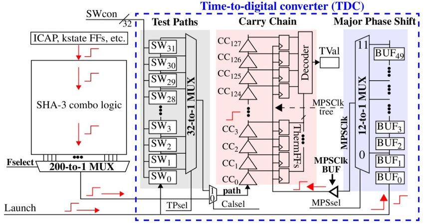
Cryptography 2018, 2, 15                                                                           2 of 17

Modern FPGAs provide on-chip battery-backed random-access memory (RAM) or E-Fuses for the
storage of a decryption key, which is used by vendor-embedded encryption hardware functions, e.g.,
the Advanced Encryption Standard (AES), within the FPGA in order to decrypt the bitstream as it is
read from the external NVM during the boot process [1]. Recent attack mechanisms have been shown to
read out embedded keys, and therefore on-chip key storage threatens the security of the boot process [2].
      In this paper, we propose a physical unclonable function (PUF)-based key generation strategy
that addresses the vulnerability of on-chip key storage. Moreover, the proposed secure boot technique
is self-contained, in that none of the FPGA-embedded security primitives or FPGA clocking resources
are utilized. We refer to the system as Bullet-Proof Boot for FPGAs (BulletProoF). BulletProoF uses
a PUF implemented in the programmable logic (PL) side of an FPGA to generate the decryption
key at boot time, and then uses the key for decrypting an off-chip NVM-stored second stage boot
image. The second stage boot image contains PL components as well as software components,
such as an operating system and applications. BulletProoF decrypts and programs the PL components
directly into those portions of the PL side that are not occupied by BulletProoF using dynamic partial
reconfiguration, while the software components are loaded into DRAM for access by the processor
system (PS). The decryption key is destroyed once this process completes, minimizing the time the
decryption key is available.
      Similar to PUF-based authentication protocols, enrollment for BulletProoF is carried out in a
secure environment. The enrollment key generated by BulletProoF is used to encrypt the second
stage boot image. Both the encrypted image and the unencrypted BulletProoF bitstreams are
stored in the NVM. During the in-field boot process, the first stage boot loader (FSBL) loads the
unencrypted BulletProoF bitstream into the FPGA. BulletProoF reads the entire set of configuration
data that has just been programmed into the FPGA using the internal configuration access port (ICAP)
interface [3], and uses this data as challenges to the PUF to regenerate the decryption key. Therefore,
BulletProoF self-authenticates. The BulletProoF bitstream instantiates the SHA-3 algorithm, and uses
this cryptographic function both to compute hashes and as the entropy source for the PUF. As we
will show, BulletProoF is designed so that the generated decryption key is irreversibly tied to the data
integrity of the entire unencrypted bitstream.
      BulletProoF is stored unencrypted in an off-chip NVM, and is therefore vulnerable to manipulation
by adversaries. However, the tamper-evident nature of BulletProoF prevents the system from booting
the components present in the second stage boot image if tampering occurs, because an incorrect
decryption key is generated. In such cases, the encrypted bitstring is not decrypted and remains secure.
      The hardware-embedded delay PUF (HELP) is leveraged in this paper as a component of the
proposed tamper-evident, self-authenticating system implemented within BulletProoF. HELP measures
path delays through a CAD-tool-synthesized functional unit—in particular, the combinational
component of SHA-3 in the proposed system. Within-die variations that occur in path delays from
one chip to another allow HELP to produce a device-specific key. Challenges for HELP are two-vector
sequences that are applied to the inputs of the combinational logic that implements the SHA-3
algorithm. The timing engine within HELP measures the propagation delays of paths sensitized by
the challenges at the outputs of the SHA-3 combinational block. The digitized timing values are used
in the HELP bitstring processing algorithm, in order to generate the AES key.
      The timing engine times paths using either the fine-phase shift capabilities of the digital clock
manager on the FPGA, or by using an on-chip time-to-digital-converter (TDC) implemented using the
carry-chain logic within the FPGA. The experimental results presented in this paper are based on the
TDC strategy.
      The BulletProoF boot process is summarized as follows:

•     The first-stage boot loader (FSBL) programs the PL side with the unencrypted (and untrusted)
      BulletProoF bitstream.
•     BulletProoF reads the configuration information of the PL side (including configuration data that
      describes itself) through the ICAP, and computes a set of digests using SHA-3.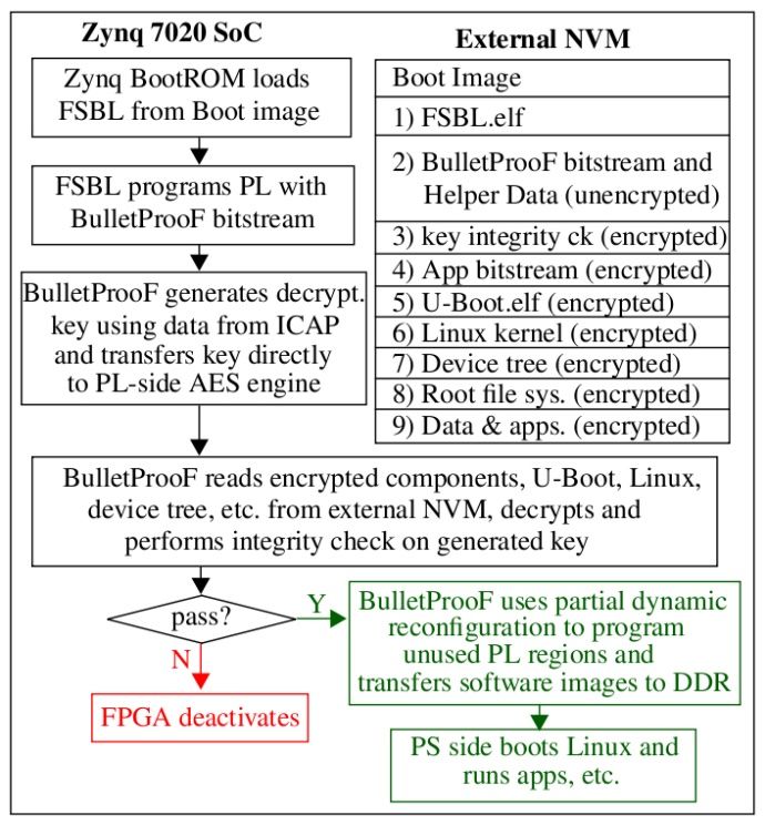
Cryptography 2018, 2, 15                                                                           3 of 17

•     For each digest, the mode of the SHA-3 functional unit is switched to PUF mode, and the HELP
      engine is started.
•     Each digest is applied to the SHA-3 combinational logic as a challenge. Signals propagate through
      SHA-3 to its outputs, and are timed by the HELP timing engine. The timing values are stored in
      an on-chip block RAM (BRAM).
•     Once all timing values are collected, the HELP engine uses them (and helper data stored in the
      external NVM) to generate a device-specific decryption key.
•     The key is used to decrypt the second stage boot image components also stored in the external
      NVM and the system boots.

     Self-authentication is ensured because any change to the configuration bitstream will change
the digest. When the incorrect digest is applied as a challenge in PUF mode, the set of paths that are
sensitized to the outputs of the SHA-3 combinational block will change (when compared to those
sensitized during enrollment using the trusted BulletProoF bitstream). Therefore, any change made by
an adversary to the BulletProoF configuration bitstring will result in missing or extra timing values in
the set used to generate the decryption key.
     The key generated by HELP is tied directly to the exact order and cardinality of the timing
values. It follows that any change to the sequence of paths that are timed will change the decryption
key. As we discuss below, multiple bits within the decryption key will change if any bit within the
configuration bitstream is modified by an adversary, because of the avalanche effect of SHA-3 and
because of a permutation process used within HELP to process the timing values into a key. Note that
other components of the boot process, including the first-stage boot loader (FSBL), can also be included
in the secure hash process, as well as FPGA-embedded security keys, as needed.
     The rest of this paper is organized as follows. Related work is discussed in Section 2. An overview
of the existing Xilinx boot process is provided in Section 3. Section 4 describes the proposed
BulletProoF system, while Section 5 describes BulletProoF countermeasures, including an on-chip
time-to-digital-converter (TDC), which leverages the carry-chain component within an FPGA for
measuring path delays. Section 6 presents a statistical analysis of bitstrings generated by the TDC as
proof-of-concept. Conclusions are provided in Section 7.

2. Background
      Although FPGA companies embed cryptographic primitives to encrypt and authenticate
bitstreams as a means of inhibiting reverse engineering and fault injection attacks, such attacks
continue to evolve. For example, a technique that manipulates cryptographic components embedded
in the bitstream as a strategy to extract secret keys is described in [4]. A fault injection attack on an
FPGA bitstream is described in [5] to accomplish the same goal, where faulty cipher texts are generated
by fault injection and then used to recover the keys. A hardware Trojan insertion strategy is described
in [6] that is designed to weaken FPGA-embedded cryptographic engines.
      There are multiple ways to store the secret cryptographic keys in an embedded system. While one
of the conventional methods is to store them in non-volatile memory (NVM), Konopinski and
Kenyon [7] and others [8] discuss several ways to extract cryptographic keys stored in NVMs,
which makes these schemes insecure. Battery-backed RAM (BBRAM) and E-Fuses are also used
for storing keys in FPGAs. BBRAMs complicate and add cost to a system design because of the
inclusion and limited lifetime of the battery. E-Fuses are one-time-programmable (OTP) memory,
and are vulnerable to semi-invasive attacks designed to read out the key via scanning technologies [8].
These types of issues and attacks on NVMs are mitigated by physical unclonable functions (PUFs),
which do not require a battery and do not store secret keys in digital form on the chip [9].
Cryptography 2018, 2,
Cryptography 2018, 3, 15
x FOR PEER REVIEW 44 of
of 17
17
3. Overview of a Secure Boot under Xilinx
3. Overview of a Secure Boot under Xilinx
A hardwired 256‐bit AES decryption engine is used by Xilinx to protect the confidentiality of
A hardwired
externally 256-bit AES
stored bitstreams [1].decryption
Xilinx providesengine is used tools
software by Xilinx to protect
to allow the confidentiality
a bitstream to be encrypted of
externally stored bitstreams [1]. Xilinx provides software tools to
using either a randomly generated or user‐specified key. Once generated, the decryption key can be allow a bitstream to be encrypted
using either
loaded through a randomly
JTAG into generated or user-specified
a dedicated E‐Fuse NVM key. Once generated, theBRAM
or battery‐backed decryption key canThe
(BBRAM). be
loaded through
power‐up JTAG into aprocess
configuration dedicated E-Fuse NVM
associated withorfielded
battery-backed
systems BRAM (BBRAM). The
first determines power-up
whether the
configuration
external bitstreamprocess associated
includes with fielded systems
an encrypted‐bitstream first determines
indicator, and if so,whether
decrypts thethe
external
bitstreambitstream
using
includes
cipher an encrypted-bitstream
block chaining (CBC) mode indicator,
of AES.and To ifprevent
so, decrypts the bitstream
fault injection using
attacks [5],cipher
Xilinxblock chaining
authenticates
(CBC) mode ofdata
configuration AES.asTo it prevent
is loaded. fault injection attacks
In particular, a 256‐bit[5], keyed
Xilinx hashed
authenticates
message configuration
authentication datacode
as it
is loaded. In particular, a 256-bit keyed hashed message authentication
(HMAC) of the bitstream is computed, using SHA‐256 to detect tamper and to authenticate the code (HMAC) of the bitstream
is computed,
sender of the using
bitstream.SHA-256 to detect tamper and to authenticate the sender of the bitstream.
During provisioning,
provisioning,Xilinx Xilinxsoftware
software is used to compute
is used to computean HMAC of the unencrypted
an HMAC bitstream,
of the unencrypted
which is then
bitstream, which embedded in the bitstream
is then embedded in theitself and encrypted
bitstream by AES. A by
itself and encrypted second
AES.HMACA second is computed
HMAC is
in the fieldin
computed asthethefield
bitstream
as theisbitstream
decrypted, and compared
is decrypted, and with
comparedthe HMACwith theembedded in the decrypted
HMAC embedded in the
bitstream. If the comparison fails, the FPGA is deactivated. The
decrypted bitstream. If the comparison fails, the FPGA is deactivated. The security propertiessecurity properties associated with the
Xilinx bootwith
associated processthe enable the detection
Xilinx boot of transmission
process enable the detection failures, and attempt
of transmission to program
failures, the FPGA
and attempt to
with
programa non-authentic
the FPGA with bitstream and tamper
a non‐authentic attacks on
bitstream andthe authentic
tamper bitstream.
attacks on the authentic bitstream.
The secure
secure boot bootmodelmodelininmodernmodern Xilinx
Xilinx system-on-chip
system‐on‐chip (SoC)(SoC) architectures
architectures differsdiffers
fromfrom
that
that described
described above, above, because
because Xilinx
Xilinx SoCs SoCs integrate
integrate bothbothprogrammable
programmablelogic logic(PL)
(PL) andand processor
components (PS).
components (PS). Moreover, the SoC is designed to be processor-centric, processor‐centric, i.e., the boot process and
overall operation
operation of of the
theSoCSoCisiscontrolled
controlledby bythetheprocessor.
processor.Xilinx XilinxSoCsSoCs use
use public
public keykeycryptography
cryptography to
carry
to carryoutoutauthentication
authentication during
during thethesecure
securebootbootprocess.
process.The Thepublic
publickeykeyisisstored
stored inin an
an NVM
NVM and is
used to authenticate configuration
configuration files, files, including
including the the first‐stage
first-stage bootboot loader
loader (FSBL),
(FSBL), and and therefore,
therefore,
the key provides secondary authentication and primary attestation.
The Xilinx Zynq 7020 SoC used in this paper incorporates both a processor (PS) side and
programmable logic (PL) side. The The processor
processor side side runs
runs an operating system (OS), e.g., Linux, and
applications on
applications on a dual core ARM cortex A‐9 A-9 processor, which is tightly coupled with the PL side
through an AMBA AXI interconnect.
The flow diagram shown on the left side of Figure 1 identifies the basic elements of the Xilinx
Zynq SoCSoCsecure
secureboot bootprocess.
process. TheTheXilinx BootROM
Xilinx BootROM loads the FSBL
loads from an
the FSBL fromexternal NVM toNVM
an external DRAM. to
The FSBL programs the PL side and then reads the second-stage
DRAM. The FSBL programs the PL side and then reads the second‐stage boot loader (U‐Boot), which boot loader (U-Boot), which is
copied
is copied to DRAM,
to DRAM, and and
passes control
passes to U-Boot.
control U-BootU‐Boot
to U‐Boot. loads the software
loads images, which
the software images, can include
which cana
bare-metal
include application,
a bare‐metal or the Linux
application, orOS,
theas well as
Linux OS,other embedded
as well as othersoftware
embedded applications
softwareand data files.
applications
A
andsecure
databoot
files.first establishes
A secure a rootestablishes
boot first of trust, and thenof
a root performs
trust, and authentication
then performs on authentication
top of the trusted onbase
top
at each
of of the subsequent
the trusted base at each stages
of theof the boot process.
subsequent stages Asofmentioned, Rivest–Shamir–Adleman
the boot process. As mentioned, Rivest– (RSA)
is used for authentication
Shamir–Adleman (RSA) and attestation
is used of the FSBL and
for authentication and other configuration
attestation of the files.
FSBLThe and
hardwired
other
256-bit AES engine
configuration files.andTheSHA-256
hardwired are then usedAES
256‐bit to securely
engine decrypt
and SHA‐256and authenticate
are then boot usedimages using
to securely
a BBRAM
decrypt andorauthenticate
E-Fuse embedded key. Therefore,
boot images using a BBRAM the root orof trust embedded
E‐Fuse and the entire key.secure boot the
Therefore, process
root
depends
of trust and on the confidentiality of the embedded keys.
entire secure boot process depends on the confidentiality of the embedded keys.
Figure
Figure 1.
1. Xilinx
Xilinx Zynq
Zynq SoC
SoC boot
boot process.
process.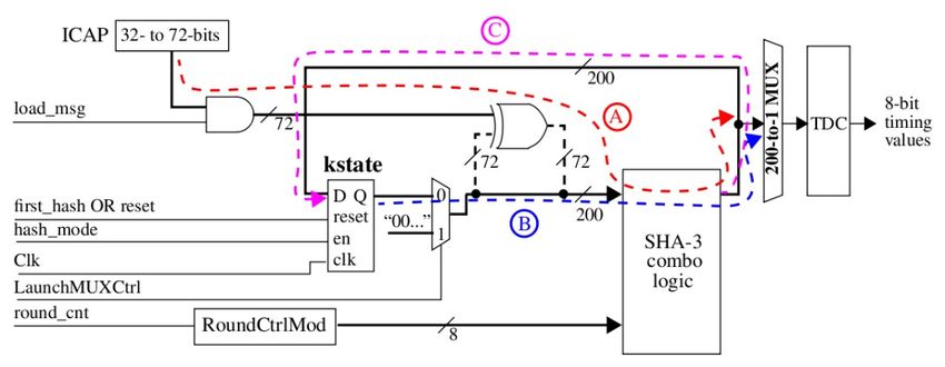
Cryptography 2018, 2, 15 5 of 17
Cryptography 2018, 3, x FOR PEER REVIEW 5 of 17
Cryptography 2018, 3, x FOR PEER REVIEW 5 of 17
4. Overview of BulletProoF
4. Overview of BulletProoF
4. Overview
BulletProoF of BulletProoF
is designed to be self‐contained, utilizing only components typically available in
BulletProoF is designed to be self-contained, utilizing only components typically available in the
the FPGA PL fabric. Specialized, vendor‐supplied embedded security components, including
FPGA PLBulletProoF is designed
fabric. Specialized, to be self‐contained,
vendor-supplied embedded utilizing only
security components
components, typicallyE-Fuse,
including available in
BBRAM,
E‐Fuse,
the FPGABBRAM,PL and
fabric. cryptographic
Specialized, primitives
vendor‐supplied like AES are
embedded not used.
security The BulletProoF
components, boot‐up
including
and cryptographic primitives like AES are not used. The BulletProoF boot-up process is illustrated in
process
E‐Fuse, is illustrated in cryptographic
Figure 2 as a flow diagram. Similar to the Xilinx
used.boot process, the BootROM
Figure
loads
as aBBRAM,
2 the and
flow diagram. Similar to theprimitives
Xilinx boot like AES are
process, thenot
BootROM The
loadsBulletProoF
the FSBL, boot‐up
which then
process is illustrated in Figure 2 as a flow diagram. Similar to the Xilinx boot process, theBulletProoF
FSBL, which then programs the PL side, in this case with the unencrypted BootROM
programs
bitstream.the PL side, in this case with the unencrypted BulletProoF bitstream. The FSBL then hands control
loads the The FSBL, FSBL thenthen
which hands control the
programs overPLto side,
BulletProoF, which
in this case withcarries out some of the
the unencrypted functions
BulletProoF
over to BulletProoF, which
normally carries out some of the functions
first task normally delegated to U-Boot. BulletProoF’s
bitstream.delegated
The FSBL thento U‐Boot. BulletProoF’s
hands control over to BulletProoF, is which
to regenerate
carries outthe somedecryption key. It
of the functions
first task is
accomplishes to regenerate
this by to the
reading decryption key.
all BulletProoF’s It accomplishes
of the configuration this
information by reading
programmed all of the configuration
into the PL
normally delegated U‐Boot. first task is to regenerate the decryption key.side
It
information
accomplishes this by reading all of the configuration information programmed into the PL side it is
using the programmed
ICAP interface into the
[3]. As PL side using
configuration thedataICAPis interface
read, it is [3].
usedAs configuration
as a challenge data
to is
time read,
paths
used as a the
between
using challenge
the
ICAPICAP to time
and paths
interface the between
[3].SHA‐3
As the ICAP
functional
configuration and
unit
data the
is(see SHA-3
read,Figure functional
3), and
it is used as a as unit (see to
inputs
challenge Figure
to the 3),
time and as
SHA‐3
paths
inputs to the
cryptographic SHA-3hash cryptographic
function to hash
compute function
a to
chained compute
set of a chained
digests.
between the ICAP and the SHA‐3 functional unit (see Figure 3), and as inputs to the SHA‐3 set of digests.
cryptographic hash function to compute a chained set of digests.
Figure2.2. Proposed
Figure Proposed Zynq
Zynq SoC
SoCboot
bootprocess.
process.
Figure 2. Proposed Zynq SoC boot process.
Figure
Figure3.3. BulletProoF
3.BulletProoF enrollment
BulletProoF enrollment and regeneration
enrollment and regeneration process.
Figure and regenerationprocess.
process.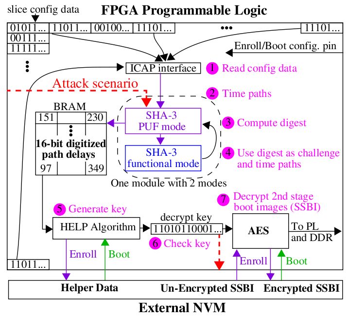
Cryptography 2018, 2, 15                                                                             6 of 17

      As configuration data is read and hashed, BulletProoF periodically changes the mode of SHA-3
from hash mode to a specialized PUF mode of operation. PUF mode configures SHA-3 such that the
combinational logic of SHA-3 is used as a source of entropy for key generation. The HELP PUF uses
each digest as a challenge to the SHA-3 combinational logic block. HELP measures and digitizes the
delays of paths sensitized by these challenges at high resolution and stores them in an on-chip BRAM
for later processing. The same timing operation is carried out for paths between the ICAP and SHA-3
outputs, as discussed above, and Field-programmable gate arrays the timing data combined and stored
with the SHA-3 timing data in the BRAM. This process continues with additional configuration data
added to the existing hash (chained), until all of the configuration data is read and processed.
      BulletProoF then reads the externally stored Helper Data and delivers it to the HELP algorithm
as needed during the key generation process that follows. The decryption key is transferred to an
embedded PL-side AES engine. BulletProoF reads the encrypted second stage boot image components
(labeled 3 through 9 in Figure 2) from the external NVM and transfers them to the AES engine.
      An integrity check is performed at the beginning of the decryption process as a mechanism to
determine if the proper key was regenerated. The first component decrypted is the key integrity
check component (labeled 3 in Figure 2). This component can be an arbitrary string or a secure hash
of, for instance, U-Boot.elf, which is encrypted during enrollment and stored in the external NVM.
An unencrypted version of the key integrity check component is also stored as a constant in the
BulletProoF bitstream. The integrity of the decryption key is checked by comparing the decrypted
version with the BulletProoF version. If they match, then the integrity check passes and the boot
process continues. Otherwise, the FPGA is deactivated and the secure boot fails.
      If the integrity check passes, BulletProoF then decrypts and authenticates components 4 through
9 in Figure 2 using 256-bit AES in CBC mode and HMAC, resp., starting with the application (App)
bitstream. An application bitstream is programmed into the unused components of the PL side
by BulletProoF, using dynamic partial reconfiguration. BulletProoF then decrypts the software
components, e.g., Linux, etc. and transfers them to U-Boot. The final step is to bootstrap the processor
to start executing the Linux OS (or bare-metal application).

4.1. BulletProoF Enrollment Process
     BulletProoF uses a physical unclonable function (PUF) to generate the decryption key, as a
mechanism for eliminating the vulnerabilities associated with on-chip key storage. Key generation
using PUFs requires an enrollment phase, which is carried out in a secure environment, i.e., before the
system is deployed to the field. During enrollment, when the key is generated for the first time, HELP
generates the key internally and transfers helper data off of the FPGA. As shown in Figure 2, the helper
data is stored in the external NVM unencrypted. The internally generated key is then used to encrypt
the other components of the external NVM (second-stage boot image, or SSBI) by configuring AES in
encryption mode.
     BulletProoF uses a configuration I/O pin (or an E-Fuse bit) to determine whether it is operating in
Enroll mode or Boot mode. The pin is labeled “Enroll/Boot config. pin” in Figure 3. The trusted party
configures this pin to Enroll mode, in order to process the “UnEncrypted SSBI” to an “Encrypted SSBI”,
and to create the helper data. The Encrypted SSBI and helper data are stored in an External NVM
and later used by the fielded version to boot (see “Enroll” annotations along the bottom of Figure 3).
Therefore, the Enroll and Boot versions of BulletProoF are identical. Note that the “Enroll/Boot config.
pin” allows the adversary through board-level modifications, in order to create new versions of the
Encrypted SSBI, but the primary goal of BulletProoF, i.e., to protect the confidentiality and integrity of
the trusted authority’s second-stage boot image, is preserved.

4.2. BulletProoF Fielded Boot Process
    A graphical illustration of the secure boot process carried out by the fielded device is illustrated in
Figure 3. As indicated above, the FSBL loads the unencrypted version of BulletProoF from the external
Cryptography 2018, 2, 15 7 of 17
NVM into the PL of the FPGA, and hands over control to BulletProoF. As discussed further below,
BulletProoF utilizes a ring oscillator as a clock source that cannot be disabled during the boot process
once it is started. This prevents attacks that attempt to stop the boot process at an arbitrary point
in order to reprogram portions of the PL using external interfaces, e.g., PCAP, SelectMap, or JTAG.
The steps and annotations in Figure 3 are defined as follows:
1. BulletProoF reads configuration data using the ICAP interface, using a customized controller.
2. Every n-th configuration word is used as a challenge to time paths between the ICAP and the
SHA-3 outputs with SHA-3 configured in PUF mode (this is done to prevent a specific type
of reverse-engineering attack, discussed later.). The digitized timing values are stored in an
on-chip BRAM.
3. The remaining configuration words are applied to the inputs of SHA-3 in functional mode to
compute a chained sequence of digests.
4. Periodically, the existing state of the hash is used as a challenge with SHA-3 configured in
PUF mode, to generate additional timing data. The digitized timing values are stored in an
on-chip BRAM.
5. Once all configuration data is processed, the HELP algorithm processes the digitized timing
values into a decryption key using helper data, which are stored in an external NVM.
6. BulletProoF runs an integrity check on the key.
7. BulletProoF reads the encrypted second-stage boot image (SSBI) from the external NVM.
AES decrypts the image and transfers the software components to U-Boot, and the hardware
components into the unused portion of the PL, using dynamic partial reconfiguration.
Once completed, the system boots.
4.3. Security Properties
The primary goal of BulletProoF is to protect the second-stage boot images, i.e., prevent them
from being decrypted, changed, encrypted, and installed back into the fielded system. The proposed
system has the following security properties in support of this objective:
• The enrollment and regeneration process proposed for BulletProoF never reveals the key outside
the FPGA. Therefore, physical, side-channel-based attacks are necessary in order to steal the key.
We do not address side-channel attacks in this paper, but it is possible to design the AES engine
with side-channel attack resistance using circuit countermeasures, as proposed in [10].
• Any type of tampering with the unencrypted BulletProoF bitstream or helper data by an adversary
will only prevent the key from being regenerated, and a subsequent failure of the boot process.
Note that it is always possible to attack a system in this fashion, i.e., by tampering with the
contents stored in the external NVM, independent of whether it is encrypted or not.
• Any attempt to reverse-engineer the unencrypted bitstream, in an attempt to insert logic between
the ICAP and SHA-3 input, will change the timing characteristics of these paths, resulting in
key regeneration failure. For example, the adversary may attempt to rewire the input to SHA-3,
in order to allow external configuration data (constructed to exactly model the data that exists in
the trusted version) to be used instead of the ICAP data.
• The adversary may attempt to reverse-engineer the helper data to derive the secret key.
As discussed in [11], the PUF used by BulletProoF uses a helper data scheme that does not
leak information about the key.
• The proposed secure boot scheme stores an unencrypted version of the BulletProoF bitstream,
and therefore, adversaries are free to change components of BulletProoF or add additional
functionality to the unused regions in the PL. As indicated, changes to configuration data read
from ICAP are detected, because the paths that are timed by the modified configuration data are
different, which causes key regeneration failure.Cryptography 2018, 3, x FOR PEER REVIEW 8 of 17
Cryptography 2018, 2, 15 8 of 17
BulletProoF uses a ring oscillator as a clock source. Therefore, once BulletProoF is started, it
cannot be stopped by the adversary as a mechanism for stealing the key (this attack is
• elaborated on
BulletProoF below).
uses a ring oscillator as a clock source. Therefore, once BulletProoF is started, it cannot
BulletProoF
be stopped bydisables the external
the adversary programming
as a mechanism interfaces
for stealing (PCAP,
the key SelectMap,
(this attack and JTAG)
is elaborated prior
on below).
• to starting todisables
BulletProoF preventthe
adversaries from attempting
external programming to perform
interfaces (PCAP,dynamic partialand
SelectMap, reconfiguration
JTAG) prior
during
to thetoboot
starting process.
prevent BulletProoF
adversaries from actively
attemptingmonitors the state
to perform dynamicof these external
partial interfaces
reconfiguration
during the boot, and destroys the timing data and keys if any changes are detected.
during the boot process. BulletProoF actively monitors the state of these external interfaces during
BulletProoF
the boot, anderases the the
destroys timing data
timing from
data andthe BRAM
keys if anyonce the key
changes areisdetected.
generated, and destroys the
• BulletProoF erases the timing data from the BRAM once the key is generated,ifand
key once the second‐stage boot image is decrypted. The key is also destroyed the key integrity
destroys the
check fails.
key once the second-stage boot image is decrypted. The key is also destroyed if the key integrity
check fails.
5. Additional BulletProoF Countermeasures
5. Additional BulletProoF Countermeasures
The primary threat to BulletProoF is key theft. This section discusses two important attack
scenarios, as well as
The primary countermeasures
threat to BulletProoF designed to dealThis
is key theft. withsection
them. discusses two important attack
scenarios, as well as countermeasures designed to deal with them.
5.1. Internal Configuration Access Port Data Spoofing Countermeasure
5.1. Internal Configuration Access Port Data Spoofing Countermeasure
The first important attack scenario is shown by the red dotted lines in Figure 3. The top left
The
dotted line firstlabeled
important“Attackattack scenario represents
scenario” is shown byan theadversarial
red dotted modification,
lines in Figurewhich 3. The is
topdesigned
left dotted
to
line labeled
re‐route the“Attack
origin of scenario” represents an
the configuration adversarial
data from themodification,
ICAP to I/Owhich pins. is
Withdesigned to re-route
this change, the
the origin of
adversary canthe configuration
stream data from
in the expected the ICAP todata,
configuration I/O and
pins.then
With this change,
freely modify any the adversary
portion of can
the
stream in the expected configuration data, and then freely modify
BulletProoF configuration. The simplest change one can make is to add a key leakage channel, as any portion of the BulletProoF
configuration.
shown by the red Thedotted
simplest change
line alongonethe can
bottommakeofisthe
to figure.
add a key leakage channel, as shown by the red
dotted line along the bottom of the figure.
The countermeasure to this attack is to ensure that the adversary is not able to make changes to
The countermeasure
the paths between the ICAP to this
andattack is to ensure
the SHA‐3, that the
without adversary
changing is not able
the timing to and
data make changes tokey.
decryption the
paths
A blockbetween
diagram the of
ICAPthe and the SHA-3,
BulletProoF without changing
architecture the timing
that addresses thisdata andisdecryption
threat shown in key. A block
Figure 4. In
diagram of the BulletProoF architecture that addresses this threat is
particular, timing data is collected by timing the paths identified as “A” and “B”. For “A”, the shown in Figure 4. In particular,
timing data is
two‐vector collected(challenge)
sequence by timing the V1–Vpaths
2 is identified as “A” and
derived directly from“B”.theFor ICAP“A”, the two-vector
data. sequence
In other words, the
(challenge) V1 –V2 is derived
launch of transitions along the directly from the
“A” paths ICAP data. Inwithin
is accomplished other words,
the ICAP theinterface
launch ofitself.
transitions
Signal
along the “A”
transitions paths is on
emerging accomplished
the ICAP outputwithinregister
the ICAP interface through
propagate itself. Signal transitions
the SHA‐3 emerging on
combinational the
logic
ICAP
to the output register propagate
time‐to‐digital converter through
(TDC) shownthe SHA-3
on thecombinational
right (discussed logicbelow).
to the time-to-digital converter
The timing operation is
(TDC) shown on the right (discussed below). The timing operation
carried out by de‐asserting hash_mode, and then launching V2 by asserting ICAP control signals using is carried out by de-asserting
hash_mode,
the ICAP input and then launching
register V2 by asserting
(not shown). The path ICAP control
selected by signals using MUX
the 200‐to‐1 the ICAP input by
is timed register (not
the TDC.
shown). The path
This operation selected to
is repeated byenable
the 200-to-1 MUX
all of the 72isindividual
timed by paths the TDC.along Thistheoperation
“A” routeis to repeated
be timed.to
enable all of the 72 individual paths along the “A” route to be timed. Note
Note that the ICAP output register is only 32 bits, which is fanned out to 72 bits, as required by the that the ICAP output register
is only 32 bits,
keccak‐f[200] whichof
version is SHA‐3
fanned[12]. out to 72 bits, as required by the keccak-f[200] version of SHA-3 [12].
Figure 4.4.Implementation
Implementation details
details of internal
of the the internal configuration
configuration access access port and
port (ICAP) (ICAP) andinterface,
SHA-3 SHA‐3
interface,
with with annotations
annotations showing
showing paths that paths that (“A”
are timed are timed (“A”and
and “B”) andhash
“B”)mode
and hash mode (“C”).
(“C”).
The timing operation involving the “chained” sequence of hashes’ time paths along the routes is
The timing operation involving the “chained” sequence of hashes’ time paths along the routes
labeled “B” in Figure 4. The current state of the hash is maintained in kstate when hash_mode is
is labeled “B” in Figure 4. The current state of the hash is maintained in kstate when hash_mode isCryptography2018,
Cryptography 2018,2,
3,15
x FOR PEER REVIEW 99 of
of 17
17
deasserted, by virtue of disabling updates to the flip‐flops (FFs), using the en input. Vector V1 of the
deasserted, by virtue is
two‐vector sequence ofall
disabling
0s, and updates
the launchto the
of Vflip-flops (FFs), using
2 is accomplished the en input.LaunchMUXCtrl.
by deasserting Vector V1 of the
two-vector sequence is all 0s, and the launch of V is accomplished by deasserting
The hash mode of operation, labeled “C”2 in Figure 4, is enabled by asserting hash_mode. LaunchMUXCtrl.
The hash data
Configuration modeis of operation,
hashed into thelabeled
current“C” in Figure
state 4, is enabled
by asserting load_msg by on asserting hash_mode.
the first cycle of the
Configuration data is hashed into the current state by
SHA‐3 hash operation. LaunchMUXCtrl remains de‐asserted in hash mode. asserting load_msg on the first cycle of the
SHA-3 hash operation. LaunchMUXCtrl remains de-asserted in hash mode.
5.2. Clock Manipulation Countermeasure
5.2. Clock Manipulation Countermeasure
The adversary may attempt to stop BulletProoF, either during key generation or after the key is
The adversary may attempt to stop BulletProoF, either during key generation or after the key is
generated; reprogram portions of the PL; or create a leakage channel that provides direct access to
generated; reprogram portions of the PL; or create a leakage channel that provides direct access to the
the key. The clock source and other inputs to the Xilinx digital clock manager (DCM), including the
key. The clock source and other inputs to the Xilinx digital clock manager (DCM), including the fine
fine phase‐shift functions used by HELP to time paths, therefore represent an additional
phase-shift functions used by HELP to time paths, therefore represent an additional vulnerability [13].
vulnerability [13].
AA countermeasure
countermeasure that that addresses
addresses clock
clock manipulation
manipulation attacksattacks is is to
to use
use aa ring
ring oscillator
oscillator (RO)
(RO) to to
generate
generate the clock and a time‐to‐digital‐converter (TDC), as an alternative path timing method that
the clock and a time-to-digital-converter (TDC), as an alternative path timing method that
replaces
replacesthe
theXilinx DCM.
Xilinx DCM. TheTheRO RO
and andTDC TDC
are implemented
are implemented in the programmable
in the programmablelogic, andlogic,
therefore
and
the configuration
therefore information
the configuration associated associated
information with them is alsothem
with processed
is alsoand validated
processed and byvalidated
the hash-based
by the
self-authentication mechanism described
hash‐based self‐authentication mechanism earlier.
described earlier.
As
As discussed previously, HELP measures path
discussed previously, HELP measures path delays
delays inin the
the combinational
combinational logic logic of
of the
the SHA-3
SHA‐3
hardware
hardware instance. The left side of the block‐level diagram in Figure 5 shows an instance of
instance. The left side of the block-level diagram in Figure 5 shows an instance of SHA-3
SHA‐3
configured
configured with components that were described in the previous section (Figure 4). The right side
with components that were described in the previous section (Figure 4). The right side
shows
shows anan embedded
embedded time-to-digital
time‐to‐digital converter
converter (TDC)
(TDC) engine,
engine, with
with components
components labeledlabeled “Test
“Test Paths”,
Paths”,
“Carry
“CarryChain”,
Chain”,and
and“Major
“MajorPhase PhaseShift”,
Shift”, which
which areareused
used to
toobtain
obtainhigh-resolution
high‐resolution measurements
measurements of of
the SHA-3 path delays.
the SHA‐3 path delays.
Figure 5.
Figure 5. Functional
Functional unit
unit and
and time-to-digital
time‐to‐digital converter
converter (TDC)
(TDC) engine
engine architecture.
architecture.
The white‐ and orange‐colored routes and elements in the Xilinx “implementation view”
The white- and orange-colored routes and elements in the Xilinx “implementation view” diagram
diagram of Figure 6 highlight carry‐chain (CARRY4) components within the FPGA that are
of Figure 6 highlight carry-chain (CARRY4) components within the FPGA that are leveraged within the
leveraged within the TDC. A CARRY4 element is a sequence of four high‐speed hardwired buffers,
TDC. A CARRY4 element is a sequence of four high-speed hardwired buffers, with outputs connected
with outputs connected to a set of four FFs, labeled “ThermFFs” in Figures 5 and 6. The carry‐chain
to a set of four FFs, labeled “ThermFFs” in Figures 5 and 6. The carry-chain component in Figure 5 is
component in Figure 5 is implemented by connecting a sequence of 32 CARRY4 primitives in a
implemented by connecting a sequence of 32 CARRY4 primitives in a series, with individual elements
series, with individual elements labeled as CC0 to CC127 in Figure 5. Therefore, the carry‐chain
labeled as CC0 to CC127 in Figure 5. Therefore, the carry-chain component implements a delay chain
component implements a delay chain with 128 stages. The path to be timed (labeled “path” in
with 128 stages. The path to be timed (labeled “path” in Figures 5 and 6) drives the bottom-most
Figures 5 and 6) drives the bottom‐most CC0 element of the carry chain. Transitions on this path
CC0 element of the carry chain. Transitions on this path propagate upwards at high speed along
propagate upwards at high speed along the chain, where each carry‐chain element adds
the chain, where each carry-chain element adds approximately 15 ps of buffer delay. As the signal
approximately 15 ps of buffer delay. As the signal propagates, the D inputs of the ThermFFs change
from 0 to 1, one by one, over the length of the chain. The ThermFFs are configured asCryptography 2018, 2, 15 10 of 17
Cryptography 2018, 3, x FOR PEER REVIEW 10 of 17
Cryptography 2018, 3, x FOR PEER REVIEW
propagates, the D inputs of the ThermFFs change from 0 to 1, one by one, over the length of the 10 of 17
chain.
positive‐edge‐triggered
The ThermFFs are configured FFs, and therefore, they sample FFs,
as positive-edge-triggered the D input
and when they
therefore, their sample
Clk input
the is
D 0. The
input
positive‐edge‐triggered FFs, and therefore, they sample the D input when their Clk input is 0. The
Clk input to the ThermFFs is driven by a special major phase shift Clk (MPSClk) that is described
when their Clk input is 0. The Clk input to the ThermFFs is driven by a special major phase shift Clk
Clk input to the ThermFFs is driven by a special major phase shift Clk (MPSClk) that is described
further below.
(MPSClk) that is described further below.
further below.
Figure 6.
Figure 6. Xilinx
Xilinx slice
slice with
with aa CARRY4
CARRY4 primitive.
primitive.
Figure 6. Xilinx slice with a CARRY4 primitive.
The delay of a path through the SHA‐3 combinational logic block is measured as follows. First,
The
The delay
delay of of aa path
path through
through the the SHA-3
SHA‐3 combinational
combinational logic block is measured as follows. First,
the MPSClk signal at the beginning of the path delay test is set to 0, in order to make the ThermFFs
the MPSClk
the MPSClk signal at the beginning
beginning of the path delay test is set to
to 0,
0, in
in order
order to
to make
make thethe ThermFFs
ThermFFs
sensitive to the delay chain buffer values. The path to be timed is selected using Fselect, and is forced
sensitive
sensitive to to the
the delay
delay chain
chain buffer values. The path to be timed is selected using Fselect, and is forced
buffer values. forced
to 0 under the first vector (V1) of the two‐vector sequence. Therefore, the path signal and the delay
to
to 00 under
under thethe first
first vector
vector (V (V11) of
of the
the two-vector sequence. Therefore, the path signal and the delay
two‐vector sequence. delay
chain buffers are initialized to 0, as illustrated on the left side of the timing diagram in Figure 7. The
chain
chain buffers are initialized to 0, as illustrated on the left side of the timing diagram
are initialized to 0, as illustrated on the left side of the timing diagram in Figure 7. The in Figure 7.
launch event is initiated by applying V2 to the inputs of SHA‐3, while simultaneously asserting the
The
launchlaunch
event event is initiated
is initiated by applying
by applying V2 to V2the
to inputs
the inputs of SHA-3,
of SHA‐3, whilewhile simultaneously
simultaneously asserting
asserting the
Launch signal, which creates rising transitions that propagate, as shown by the red arrows on the left
the Launch
Launch signal,
signal, which which creates
creates rising
rising transitions
transitions thatthat propagate,
propagate, as shown
as shown by the
by the red red arrows
arrows on the
on the left
side of Figure 5. The Launch signal propagates into the MPS BUFx delay chain, shown on the right
left
sideside of Figure
of Figure 5. The5. The
LaunchLaunch
signal signal propagates
propagates into into
the MPS BUFxBUF
the MPS delay x delay
chain,chain,
shown shown
on theonright
the
side of Figure 5, simultaneous with the path signal’s propagation through SHA‐3 and the carry chain.
right
side of side of Figure
Figure 5, simultaneous
5, simultaneous with the withpath path signal’s
thesignal’s propagation
propagation through through
SHA‐3SHA-3
and the and thechain.
carry carry
The Launch signal eventually emerges from the major phase shift unit on the right, as MPSClk (to
chain. The Launch signal eventually emerges from the major phase shift
The Launch signal eventually emerges from the major phase shift unit on the right, as MPSClk (to unit on the right, as MPSClk
minimize Clk skew, the MPSClk signal drives a Xilinx BUFG primitive and a corresponding clock
(to minimize
minimize ClkClk skew,
skew, thethe MPSClk
MPSClk signaldrives
signal drivesa aXilinx
XilinxBUFG
BUFGprimitive
primitiveand and aa corresponding clock
tree on the FPGA.). When MPSClk goes high, the ThermFFs store a snapshot of the current state of
tree
tree on the FPGA.). When MPSClkgoes
WhenMPSClk goeshigh,
high,thetheThermFFs
ThermFFsstore
storea asnapshot
snapshot ofofthethe current
current state
state of
the carry chain buffer values. Assuming this event occurs, as the rising transition on path is still
of the carry chain buffer values. Assuming this event occurs,
the carry chain buffer values. Assuming this event occurs, as the rising transition on as the rising transition on path is still
still
propagating along the carry chain, the lower set of ThermFFs will store 1s while the upper set store
propagating
propagating along along the the carry
carry chain,
chain, the lowerlower set of of ThermFFs
ThermFFs will store 1s while while thethe upper
upper set set store
store
0s (see timing diagram in Figure 7 for an illustration). The sequence of 1s followed by 0s is referred
0s
0s (see
(see timing
timing diagram
diagram in Figure Figure 77 forfor an
an illustration).
illustration). The sequence of 1s followed by 0s is referred referred
to as a thermometer code, or TC. The decoder component in Figure 5 counts the number of 0s in the 128
to
to as a thermometer code, or TC. The decoder component in Figure 5 counts
thermometer code, or TC. The decoder component in Figure 5 counts the number of 0s in the the number of 0s in the
128
ThermFFs, and stores this count in the TVal (timing value) register. The TVal is added to an
128 ThermFFs,
ThermFFs, andand storesstores
thisthis count
count in inthethe TVal(timing
TVal (timingvalue)
value)register.
register.The TheTVal
TVal isis added
added to an an
MPSOffset (discussed below) to produce a PUF Number (PN), which is stored in BRAM for use in
MPSOffset
MPSOffset (discussed
(discussedbelow) below)totoproduce
producea aPUF PUF Number
Number (PN), which
(PN), which is stored in BRAM
is stored in BRAM for use in the
for use in
the key generation process.
key generation
the key generation process.
process.
Figure 7. Timing diagram for the timing engine.
Figure 7.
Figure 7. Timing
Timing diagram
diagram for
for the
the timing
timing engine.
engine.Cryptography 2018, 2, 15 11 of 17
5.2.1. Underflow and Overflow
The differences in the relative delays of the path and MPSClk signals may cause an underflow
or overflow error condition, which is signified when the TVal is either 0 or 128. Although the carry
chain can be extended in length as a means of avoiding these error conditions, it is not practical to
do so. This is because of a very short propagation delay associated with each carry-chain element
(approximately 15 ps), as well as the wide range of delays that need to be measured through the
SHA-3 combinational logic (approximately 10 ns), which would require the carry chain to be more
than 650 elements in length.
In modern FPGAs, a carry chain of 128 elements is trivially mapped into a small region of the
programmable logic. The shorter length also minimizes adverse effects created by across-chip process
variations, localized temperature variations, and power supply noise. However, the shorter chain does
not accommodate the wide range of delays that need to be measured, and instances of underflow and
overflow become common events.
The major phase shift (MPS) component is included as a means of dealing with underflow and
overflow conditions. Its primary function is to extend the range of the paths that can be timed. With
128 carry-chain elements, the range of path delays that can be measured is approximatelly 128 × 15 ps,
which is less than 2 ns. The control inputs to the MPS, labeled “MPSsel” in Figure 5, allow the phase
of MPSClk to be adjusted in order to accommodate the 10 ns range associated with the SHA-3 path
delays. However, a calibration process needs to be carried out at start-up, to allow continuity to be
maintained across the range of delays that will be measured.
5.2.2. Calibration
The MPS component and calibration are designed to expand the measurement range of the TDC,
while minimizing inaccuracies introduced as the configuration of the MPS is tuned to accommodate
the length of the path being timed. From Figure 5, the MPSClk drives the ThermFF Clk inputs,
and therefore controls how long the ThermFFs continue to sample the CCx elements. The 12-to-1 MUX
associated with the MPS can be controlled using the MPSsel signals, to delay the Clk with respect to
the path signal. The MPS MUX connects to the BUFx chain at 12 different tap points, with 0 selecting
the tap point closest to the origin of the BUF path along the bottom, and 11 selecting the longest path
through the BUFx chain. The delay associated with MPSsel when set to 0 is designed to be less than
the delay of the shortest path through the SHA-3 combinational logic.
An underflow condition occurs when the path transition arrives at the input of the carry chain
(at CC0 ), after the MPSClk is asserted on the ThermFFs. The MPS controller configures the MPSsel to 0
initially, and increments this control signal until underflow no longer occurs. This requires the path
to be retested at most 12 times, once of each MPSsel setting. Note that paths timed when MPSsel > 0
require an additional delay along the MPS BUFx chain, called an MPSOffset, to be added to the TVal.
Calibration is a process that determines the MPSOffset values associated with each MPSsel > 0.
The goal of calibration is to measure the delay through the MPS BUFx chain between each of the
tap points associated with the 12-to-1 MUX. In order to accomplish this, during calibration, the role of
the path and MPSClk signals are reversed. In other words, the path signal is now the ‘control’ signal
and the MPSClk signal is timed. The delay of the path signal needs to be controlled in a systematic
fashion to create the data required to compute an accurate set of MPSOffset values associated with
each MPSsel setting.
The calibration process utilizes the Test Path component from Figure 5, to allow systematic control
over the path delays. During calibration, the Calsel is set to 1, which redirects the input of the carry chain
from SHA-3 to the Test Path output. The TPsel control signals of the Test Path component allow paths
of incrementally longer lengths to be selected during calibration, from 1 LUT to 32 LUTs. Although
paths within the SHA-3 combo logic unit can be used for this purpose, the Test Path component allows
a higher degree of control over the length of the path. The components labeled SW0 through SW31
refer to a “switch”, which is implemented as two parallel 2-to-1 MUXs (similar to the arbiter PUF,Cryptography 2018, 2, 15 12 of 17
but with no constraints with regard to matching delays along the two paths [14]). The rising transition
entering the chain of switches at the bottom is fanned out, and propagates along two paths. Each SW
can be configured with a SWcon signal to either route, the two paths straight through both MUXs
(SWcon = 0), or the paths can be swapped (SWcon = 1). The configurability of the Test Path component
provides a larger variety of path lengths that the calibration can use, which improves the accuracy of
the computed MPSOffsets.
The tap points in the MPS component are selected such that any path within the Test Path
component can be timed without underflow or overflow by at least two consecutive MPSsel control
settings. If this condition is met, then calibration can be performed by selecting successively longer
paths in the Test Path component and timing each of them under two (or more) MPSsel settings.
By holding the selected test path constant and varying the MPSsel setting, the computed TVals
represent the delay along the BUFx chain within the MPS between two consecutive tap points.
Table 1 shows a subset of the results of applying calibration to a Xilinx Zynq 7020 FPGA.
The left-most column identifies the MPSsel setting (labeled MPS). The rows labeled with a number
in the MPS column give the TVals obtained for each of the test paths (TP) 0-31 under a set of SWcon
configurations from 0–7. The SWcon configurations are randomly selected 32-bit values that control
the state of Test Path switches from Figure 5. In our experiments, we carried out calibration with
eight different SWcon vectors, as a means of obtaining sufficient data to compute the set of seven
MPSOffsets accurately.
TVals of 0 and 128 indicate underflow and overflow, respectively. The rows labeled “Diffs” are
differences computed using the pair of TVals shown directly above the Diffs values in each column.
Note that if either TVal of a pair is 0 or 128, the difference is not computed, and is signified using “NA”
in the table. Only the data and differences for MPS 0 and 1 (rows 3–5) and MPS 1 and 2 (rows 6–8)
are shown from the larger set generated by the calibration. As an example, the TVals in rows 3 and 4
of column 2 are 91 and 17, respectively, which represents the shortest test path 0 delay under MPSsel
settings 0 and 1, respectively. Row 5 gives the difference as 74. The Diffs in a given row are expected
to be same because the same two MPSsel values are used. Variations in the Diffs occur because of
measurement noise and within-die variations along the carry chain, but are generally very small, e.g.,
2 or smaller, as shown by the data in the table.
The “Ave.” column on the right gives the average values of the Diffs across each row, using data
collected from eight SWcon configurations. The “MPSOffset” column on the far right is simply
computed as a running sum of the “Ave.” column values from top to bottom. Once calibration data
was available and the MPSOffset values computed, delays of paths within the SHA-3 were measured
by setting MPSsel to 0, and then carrying out a timing test. If the TVal was 128 (all 0s in the carry chain)
then the MPSClk arrived at the ThermFFs before the transition on the functional unit path arrived at
the carry chain input. In this case, the MPSsel value was incremented, and the test was repeated until
the TVal was non-zero. The MPSOffset associated with the first test of a path that produced a valid
TVal was added to the TVal, to produce the final PN value (see Figure 7).You can also read