Recent advancements and perspectives on light management and high performance in perovskite light-emitting diodes
←
→
Page content transcription
If your browser does not render page correctly, please read the page content below
Nanophotonics 2021; 10(8): 2103–2143

Review

Shaoni Kar, Nur Fadilah Jamaludin, Natalia Yantara, Subodh G. Mhaisalkar* and
Wei Lin Leong*

Recent advancements and perspectives on light
management and high performance in perovskite
light-emitting diodes
https://doi.org/10.1515/nanoph-2021-0033                                      efficiencies up to 100%. In addition, the poor ambient and
Received January 26, 2021; accepted March 9, 2021;                            operational stability of these materials and devices restrict
published online March 30, 2021                                               further commercialization efforts. With best operational
                                                                              lifetimes of only a few hours reported, there is a long way to
Abstract: Perovskite semiconductors have experienced
                                                                              go before perovskite LEDs can be perceived as reliable al-
meteoric rise in a variety of optoelectronic applications.
                                                                              ternatives to more established technologies like organic or
With a strong foothold on photovoltaics, much focus now
                                                                              quantum dot-based LED devices. This review article starts
lies on their light emission applications. Rapid progress in
                                                                              with the discussions of the mechanism of luminescence in
materials engineering have led to the demonstration of
                                                                              these perovskite materials and factors impacting it. It then
external quantum efficiencies that surpass the previously
                                                                              looks at the possible routes to achieve efficient outcoupling
established theoretical limits. However, there remains
                                                                              through nanostructuring of the emitter and the substrate.
much scope to further optimize the light propagation in-
                                                                              Next, we analyse the instability issues of perovskite-based
side the device stack through careful tailoring of the optical
                                                                              LEDs from a photophysical standpoint, taking into
processes that take place at the bulk and interface levels.
                                                                              consideration the underlying phenomena pertaining to
Photon recycling in the emitter material followed by effi-
                                                                              defects, and summarize recent advances in mitigating the
cient outcoupling can result in boosting external
                                                                              same. Finally, we provide an outlook on the possible routes
                                                                              forward for the field and propose new avenues to maxi-
Shaoni Kar and Nur Fadilah Jamaludin have contributed equally.                mally exploit the excellent light-emitting capabilities of
                                                                              this family of semiconductors.
*Corresponding authors: Subodh G. Mhaisalkar, Energy Research
Institute at Nanyang Technological University (ERI@N), Research               Keywords: light emission; light-emitting diode; light
Techno Plaza, X-Frontier Block, Level 5, 50 Nanyang Drive, Singapore          outcoupling; perovskite.
637553, Singapore; and School of Materials Science and Engineering,
Nanyang Technological University, Nanyang Avenue, 639798,
Singapore, Singapore, E-mail: subodh@ntu.edu.sg; and Wei Lin                  1 Introduction
Leong, Energy Research Institute at Nanyang Technological University
(ERI@N), Research Techno Plaza, X-Frontier Block, Level 5, 50 Nanyang
Drive, Singapore 637553, Singapore; and School of Electrical and
                                                                              Hybrid organic–inorganic metal halide perovskites have
Electronic Engineering, Nanyang Technological University, 50                  completely revolutionized the field of optoelectronics in the
Nanyang Avenue, Singapore 639798, Singapore,                                  last decade, with exponential growth in efficiency observed
E-mail: wlleong@ntu.edu.sg. https://orcid.org/0000-0002-1402-                 for both photovoltaic and light emission applications. Since
0083                                                                          the pioneering work by Miyasaka et al. [1], perovskite solar
Shaoni Kar, Energy Research Institute at Nanyang Technological
                                                                              cell efficiencies have surpassed 25% in single junction
University (ERI@N), Research Techno Plaza, X-Frontier Block, Level 5, 50
Nanyang Drive, Singapore 637553, Singapore; School of Electrical and          configuration [2]. The arrival of perovskite-based light-emit-
Electronic Engineering, Nanyang Technological University, 50 Nanyang          ting diodes (PeLEDs) in the scene in 2014 [3] has presented a
Avenue, Singapore 639798, Singapore; and Interdisciplinary Graduate           breakthrough for low-cost, high-performance emitters.
School, Nanyang Technological University, 639798, Singapore,                  PeLED efficiency trajectory has experienced a remarkable
Singapore. https://orcid.org/0000-0002-7325-1527
                                                                              surge with a pace hitherto unseen for other mature LED
Nur Fadilah Jamaludin and Natalia Yantara, Energy Research Institute
at Nanyang Technological University (ERI@N), Research Techno Plaza,
                                                                              technologies, such as organic LEDs (OLEDs) and quantum
X-Frontier Block, Level 5, 50 Nanyang Drive, Singapore 637553,                dot LEDs (QLEDs) (Figure 1). This can be attributed to the wide
Singapore                                                                     range of unique optoelectronic properties exhibited by
  Open Access. © 2021 Shaoni Kar et al., published by De Gruyter.          This work is licensed under the Creative Commons Attribution 4.0 International
License.
2104           S. Kar et al.: Light management for high-performance perovskite LEDs

perovskites such as direct bandgap [93], high defect tolerance           reported for commercial OLEDs (at initial L0 = 1000 cd m−2)
[94] and extremely high colour purity [95].                              as shown in Table 1. Therefore, improving stability will be a
     On the processing front, perovskites too present                    key step towards bringing PeLEDs closer towards real-
an advantage over other conventional emitters. Their                     world applications. In general, the degradation of LED
optoelectronic properties, in particular, the emission                   performance can be induced by both external (environ-
wavelength, can be easily tuned via solution-based                       mental) and internal factors. While external factors that
compositional and structural engineering to achieve                      accelerate degradation can be eliminated by using matured
application-specific characteristics. It is thus unsurpris-              OLED or QLED encapsulation techniques, internal factors
ing that rapid performance enhancement in PeLEDs,                        such as materials or interface instability under device
where maximum efficiency exceeding 20% for green, red                    operation, are challenges which still need to be addressed.
and near infrared (NIR) emissions, as well as the uptick in                   One of the key advantages of this class of materials is
blue emissive PeLED efficiency, has been observed in                     the ease of tuning emission wavelength (bandgap) by
recent years. The external quantum efficiency (EQE) of                   modifying one or all of its constituent elements in the
LED can be defined as the product of carrier injection                   precursor solution. Low-temperature, solution-based pro-
efficiency (ηinj), photoluminescence quantum yield                       cessing of lead halide perovskites is possible due to their
(PLQY) and light outcoupling efficiency (ηout). With de-                  ionic nature, allowing for rapid crystallization to occur
vice and materials engineering pushing state-of-the-art                  even at ambient temperatures [107]. While the ionic
PeLEDs close to their maximum theoretical efficiency in a                 bonding nature and the antibonding characteristics of the
planar bottom-emitting device configuration (ηout ≈ 20%)                  band extrema translates to relatively shallow defects (lead
[4], the only way to further the efficiency is by investing in            and halide vacancies: VPb and VX respectively) which do
structures promoting higher light outcoupling efficiency.                 not significantly contribute to non-radiative recombination
The relatively less expansive reports on incorporating                   of charge carriers [108], their low formation energy high-
outcoupling structures in PeLEDs, both internally and                    lights the need to suppress their occurrence due to their
externally, highlight the loss in efficiency potential for                propensity as initiation sites for degradation process. It has
PeLEDs. More effort should thus be directed towards                      been reported that migration of both negatively and posi-
improving light management in current PeLEDs to push                     tively charged ions can occur in the presence of point de-
the boundaries of efficiency further.                                     fects [109–111], with the process becoming more dominant
     In addition, beyond the efficiency race, PeLED                      at the surfaces and grain boundaries [112]. Aside from ion
commercialization is still hampered by its operational                   migration, these defects also facilitate the ingress of
stability which is inferior to industrial standards. In fact,            moisture and oxygen, thus increasing perovskite suscep-
the longest lifetime reported to date for initial luminance              tibility to degradation by lowering the ion migration acti-
(L0) of 100 cd m−2 to drop by 50% (T50) is in hundreds of                vation energy [113]. While ion migration may originate from
hours, which is still far from the thousands of hours                    the perovskite layer, the proliferation in the adjacent layers

Figure 1: (a) Yearly peak external quantum efficiency (EQE) growth and (b) maximum luminance as a function of EQE for red, green and blue
perovskite-based light-emitting diodes (PeLEDs) and as well as those of current lighting technologies (OLED and QLED). The data are collected
from previous studies [3–93] and are tabulated in Table 1.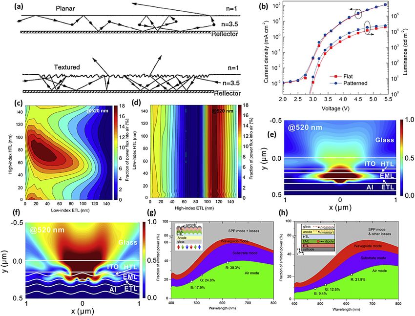
S. Kar et al.: Light management for high-performance perovskite LEDs 2105
Table : Summary of recent advances in red, blue, green and near-IR LEDs based on organic emitters, quantum dots and perovskites.
Lighting Colour Year EQE (%) Max. luminance (Cd. m−) Ref.
technology
OLED . []
– []
. – []
. – []
– []
. , []
. – []
[]
. – []
. – []
. – []
. – []
. – []
– []
[]
QLED . – []
. .
. –
. .
. –
. .
. –
. ,
. ,
. –
– []
. – []
Perovskite Blue . []
. []
. []
. . []
[]
. []
. []
. []
. . []
. []
[]
. []
. []
. []
Green . []
. , []
. , []
. – []
. []
. []
[]
. , []
. , []
. , []
. – []
. , []
. []
2106 S. Kar et al.: Light management for high-performance perovskite LEDs
Table : (continued)
Lighting Colour Year EQE (%) Max. luminance (Cd. m−) Ref.
technology
. []
. , []
. , []
. , []
. – []
. .E+ []
. , []
Red . []
. []
. []
. []
. – []
– []
. – []
. []
. []
. []
. , []
. []
. – []
. , []
Near-IR . – []
. []
. – []
. – []
. – []
. – []
. – []
. – []
. – []
. – []
. – []
OLED, organic LED; QLED, quantum dot-based LED.
during prolonged device operation [114], contributes to- and form layered [BX6] octahedral framework in between
wards PeLED degradation. single or bilayer L cations. Known as Ruddlesden-Popper
The presence of these defects and thus dominance of (RP) perovskites with a general formula of L2Am−1BmX3m+1,
monomolecular recombination also has implications on the bandgap (Eg) of the resulting material can be raised by
radiative recombination efficacy, where high charge carrier increasing the proportion of L cation (m) [120]. While the
densities are required for high PLQY to be achieved. How- creation of phase-pure RP perovskite film is challenging due
ever, the low carrier injection regime in which PeLEDs to small differences in the thermodynamic stability of the
operate in, presents a challenge to the development of high compound with increasing m values [121], the formation of
performing devices [115], underscoring the need to effec- multi-domain films with various Eg values can form a
tively concentrate and confine carriers through both phys- pseudo-quantum well landscape, which promotes energy
ical (band alignment), and/or dielectric means [69, 116–118]. transfer and charge carrier confinement to the smallest Eg
In practice, two kinds of charge carrier confinement ap- domain [118]. Aside from RP perovskite series, other quasi-
proaches have been successfully deployed viz., creation of 2D perovskite types may also be templated depending on the
quasi two-dimensional (2D) perovskite or nanocrystals cations used. When the mono-ammonium functionalized
[118, 119]. The first approach revolves around introducing ligand, typical of RP perovskite, is substituted with a bi-
bulky ammonium-functionalized cation (L) to break the functionalized alternative, Dion–Jacobson (DJ) [122] perov-
three-dimensional (3D) perovskite [BX6] octahedral network skites may crystallize. The difference in stacking motif and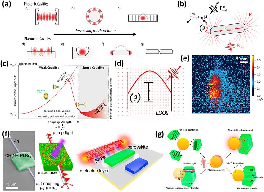
S. Kar et al.: Light management for high-performance perovskite LEDs     2107

symmetry offered by DJ molecules has been shown to impart                          dn
                                                                                      = G − k 1 n − k 2 n2 − k 3 n3          (1)
greater rigidity in perovskites [123–125] enabling higher                          dt
spectral stability to be achieved under prolonged device        where n refers to the carrier density, G denotes the rate of
operation. However, care needs to be taken in the design of     generation of charge carriers, and k1, k2 and k3 are the co-
DJ molecules to ensure that the dual binding offered does       efficients of the first-order monomolecular recombination,
not inadvertently result in formation of lattice defects.       second-order bimolecular recombination and third-order
Alternating cations in interlayer space (ACI) type of perov-    Auger recombination respectively. These occur at different
skite achieved from the use of two different types of small     excitation fluence regimes; exhibiting linear, quadratic and
A-site cations, has previously been reported for solar cell     cubic dependencies on n. Initial studies using optical-
application [126]. However, their use for light emission        pump-terahertz-probe (OPTP) photoconductivity spectros-
applications has been less extensively explored. The second     copy and photoluminescence (PL) measurements have
approach of employing nanocrystal emitters also offers          shown clear origins of these recombination events [141, 142].
charge carrier confinement effects within the crystals as        Monomolecular recombination is a direct consequence of
nanocrystal surfaces are capped with less conducting            the trapping of charges in defect states and can be seen to
ligands. Moreover, the adoption of such synthesis routes has    occur at low fluences of 1017 cm−3, is
in PeLED, analyses the defects issues and approaches to         considered to be intrinsically linked with the electronic
mitigate them. We hope to provide the readers with a            band structure of the system and is a phenomenon
roadmap of general guidelines to maximally exploit the          mandated by the requirement for energy and momentum
excellent light-emitting capabilities of this family of semi-   conservation for all charge carriers involved [140]. Typical
conductors, serving as a guide to expedite future de-           rates for k3 are of the order of 10−28 cm6 s−1 [146]. It is
velopments in the field.                                         important to note that these coefficients directly determine
                                                                the photoluminescence quantum yield (PLQY) of a perov-
                                                                skite system, which is essentially the ratio of the radiative to
                                                                total recombination rates [145]. It is expressed as,
2 The luminescence mechanism
                                                                                                   nk 2
  and underlying photophysics                                                          η=
                                                                                            k 1 + nk 2 + n2 k 3
                                                                                                                             (2)

Absorption spectra of perovskite thin films show low            This function dictates the correlation discussed above with
Urbach energies (∼15–25 meV) [135, 136], comparable to          different recombination regimes getting activated with
commercially established systems such as GaAs and c-Si          increasing fluence. Moving along from monomolecular to
(respectively, ∼7.5 and ∼10 meV) [137, 138]. In spite of        bimolecular regimes with increasing excitation density, η
having considerably high defect density [139], low ener-        increases concomitantly before peaking with n = (k1/k3)0.5.
getic disorder has also been shown to be present, thus          Furthermore, at very high carrier densities where Auger
enabling their use in various light emission applications       events dominate, η undergoes a decrease [147, 148].
[140]. Although many studies have probed and standard-               There is a discrepancy of a few orders of magnitude
ized the recombination mechanisms underlying lumines-           between n, at which η is maximum, (∼1017 cm−3) and
cence in these systems [141], it is yet to be completely        operationally feasible n values in LEDs (∼1015 cm−3) [22]. To
understood how charge injection affects perovskite in an        bridge this gap, it is hence desirable to reduce trap den-
LED device stack. The charge carrier recombination dy-          sities in the system (mainly affecting k1). On the other hand,
namics of 3D perovskites can be quantitatively described        although it is important to enhance radiative recombina-
by the rate equation [141]:                                     tion (higher k2), there is an associated broadening of the PL
2108          S. Kar et al.: Light management for high-performance perovskite LEDs

peak [149]. The routes to mitigate these in a bid to move            enhancement in EQEs of PeLEDs from an emitter material
towards higher PLQY at reasonable fluences, are twofold.              quality perspective.
The first approach is dimensional reduction of the lattice                 After ensuring near unity ηradiative of the perovskite
structure to create quantum (and/or dielectric) spatial              emitter itself, maximizing both fbalance and fe-h via rigorous
confinement such that luminescence emission can origi-                device engineering is essential to further enhance the EQE.
nate from both excitons and free carriers. The energy                In general, the choice of electron or hole injection layers
landscape is built in a way to induce higher binding energy          are adopted from the well-studied solution-processed
and create local recombination centres to promote exci-              OLEDs or conventional quantum dot-based (QD) LEDs.
tonic recombination. Thus, several quasi-2D (2D-3D)                  Indeed, with internal quantum efficiency (IQE, defined as
perovskites (such as (PEA)2PbBr4 [150], PEA2Csn−1Pbn                 product of fbalance, fe–h and ηradiative) almost reaching the
(Br/Cl)3n+1 [151] etc.), 1D (such as C4N2H14PbBr4) [152] and         limits, efficient light outcoupling management strategies
0D systems (such as Cs3Cu2I5) [153] have been investigated           will play a major role in the future to amplify the EQE.
for light emission. With highly efficient exciton self-               Strategies to enhance ηout include modifications to the
trapping yielding below-gap broadband luminescence                   design of materials and interfaces from optics point of view
[154, 155], these lower-dimensional systems are extremely            as well as external light outcouplers.
promising as emitter materials. In addition, improved                     From materials and interfaces perspectives, while
environmental and operational stability lend them                    PeLEDs have adopted similar emitter and device configu-
reliability for deployment in device application [156, 157].         ration as OLEDs, the difference between the light emission
     The second method is geometrical reduction of the               process occurring in an OLED as compared to that in a
emitter in order to obtain tuneable, colour-pure emission.           PeLED highlights the advantage of photon recycling (PR) in
To this avail, nanocrystals, quantum dots, nanowire arrays           the latter (Figure 2a). The dominance of PR in PeLED is
and several other nanostructures offering precise di-                attributed to the relatively smaller Stokes shift for perovskite
ameters, have been fabricated. These show luminous effi-             emitters as compared to organic emitters [139]. In addition,
ciencies which are not only superior to their greater-               organic emitters generally possess high exciton binding
dimensional counterparts but are also almost on par with             energies that limits the PLQY severely due to the non-
organic emitters [133]. Facile chemical and morphological            emissive nature of spin-triplet excitons in compliance with
tuneability resulting in a wide colour gamut have made               spin statistics [163]. Accumulation of triplet excitons at high
these the staple emitter materials for very highly efficient          carrier densities leads to optical losses within the system
PeLEDs recently [117, 151].                                          [164]. Several techniques such as employing triplet
     In light emission application, EQE serves as the key            quenchers [148, 165], singlet-triplet exciton annihilation
figure of merit under consideration that requires maximi-            (STA) [166], inducing delayed fluorescence by reverse
zation. A quantitative picture of the dependence of EQE on           intersystem crossing, rapid intersystem crossing etc. [147],
several parameters can be expressed as [134]:                        have been extensively used to bypass this obstacle. How-
                                                                     ever, in perovskites, such limitations do not exist due to
             EQE = fbalance × fe−h × ηradiative × ηout         (3)
                                                                     reduced excitonic interactions. In addition, owing to smaller
where fbalance denotes the probability of charge injection           emission linewidths and facile bandgap tuneability, perov-
balance, fe−h is the probability of exciton formation per            skite materials seem to enjoy a clear advantage in devices
injected carrier (an indicator of leakage current), ηradiative is    over OLEDs. The strategies to exploit PR to boost the ηout and
the radiative recombination probability for each e–h pair            overall device performances will be discussed further in the
(a.k.a PLQY of emitter material) and ηout is the light out-          next chapter (Section 2.1).
coupling efficiency. Approaches to ensure high PLQY of the                 Materials engineering on perovskite to boost the ηout
materials such as complete control of film morphology                 within the emitter itself can be carried out by manipulating
[158] and chemical composition of the emitter [136, 159] as          the transient dipole moments (TDM) of the materials [162].
well as suitable interface engineering aimed at defect               By using a formalism for quantum efficiency specified for
reduction at interfaces and grain boundaries [135] has led           organic emitters, a new figure of merit, the alignment
to the attainment of almost-unity internal PLQY in perov-            constant (ζ) is defined with consideration of the position
skites [160]. Furthermore, energy funnelling strategies              and orientation of the emissive TDM of the emitter along
introduced by employing multi-domain RP perovskite to                with their refractive indices. A concept adapted from the
create natural multi-quantum well (MQW) structures lead              field of OLEDs, the TDM method allows complete mapping
to higher ηradiative especially at lower carrier injection rate      of the energy distribution into the different optical modes
[161]. This in turn, has resulted in the plateauing of further       as well as affords close insight into the influence of other
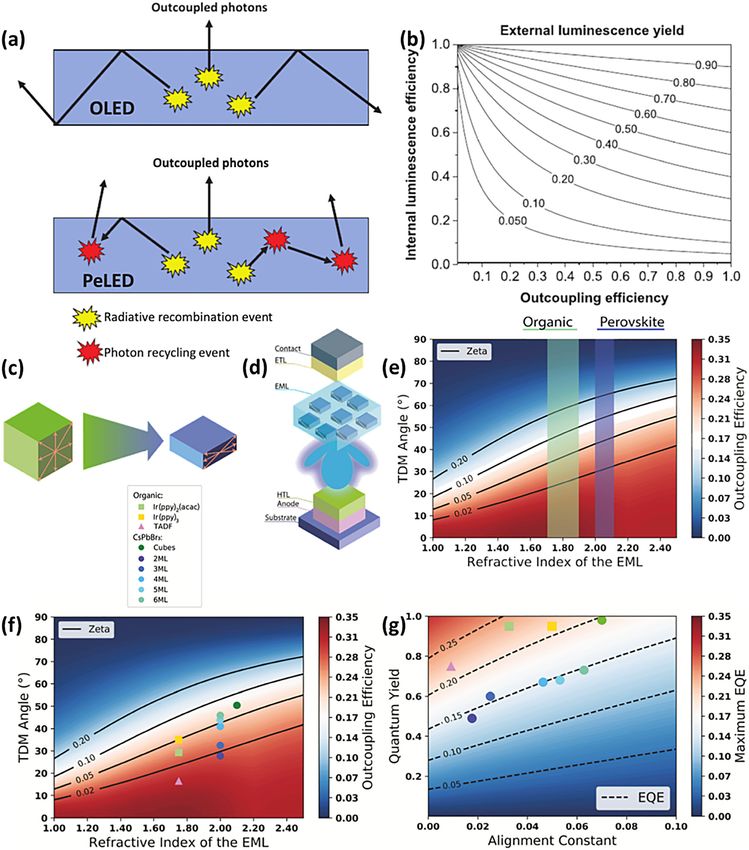
S. Kar et al.: Light management for high-performance perovskite LEDs           2109

Figure 2: (a) Schematic to compare the light outcoupling in an organic LEDs (OLED) (top) and perovskite-based light-emitting diodes (PeLED)
(bottom), with the arrows denoting photon trajectories. Large Stokes shifts in OLEDs mostly prevent reabsorption and hence minimal PR
occurs, in contrast to PeLEDs. Thus, a larger fraction of the waveguided photons are re-emitted and outcoupled in the forward direction. (b)
External luminescence yields as a function of outcoupling efficiency and internal luminescence yield calculated by considering PR processes.
TDM affecting light outcoupling in perovskite nanocrystal LEDs. Reproduced with permission from [139]. (c) Schematic of the possible
orientations of the TDM in perovskite nanocrystals. (d) Depiction of an exemplary stack design used to simulate the outcoupling efficiency of
perovskite LEDs. (e) The outcoupling efficiency dependence on the angle of the emissive TDM and the refractive index of the EML. Samples with
the same alignment constant yield identical light outcoupling efficiency, as indicated by the contour lines. Outcoupling efficiency and EQE
limits of PeLEDs. (f) The outcoupling efficiency dependence on the TDM angle and the refractive index of the EML for perovskite nanocrystals
and some prototypical organic emitters. (g) Performance of the investigated exemplary PeLED stack for different quantum yields and
alignment constants of the emissive nanocrystals. Reproduced with permission from [162].
2110        S. Kar et al.: Light management for high-performance perovskite LEDs

optical effects within/around the emitter material that can         [174]. Theoretical models predict up to 100% emission ef-
affect the ηout (Figure 2b–g). The parameter ζ not only             ficiency with PR taken into consideration. Although such
specifies the final ηout in a more holistic approach but also         values are prevented by non-ideal thermodynamic losses
contains information about the angular distribution of              in a device, PR is a key parameter that can drive up EQEs
emitted power. It is given by,                                      further. However, for ηradiative, it can also prove to be a
                                                                    primary loss mechanism. Thus, it is crucial to optimize
                                 sin2 φTDM
               ζ =                                           (4)    device design to achieve PR-assisted ηout. Recent reports
                     n4EML   − sin2 φTDM (n4EML − 1)
                                                                    hint towards deployment of nanophotonic designs along
where, ηEML is the refractive index of the emitter perovskite       with high PLQY perovskite emitters as a viable approach to
layer and ΦTDM is the angle of the emissive TDM with                achieve enhanced emission.
respect to the film surface. Thus, ζ can assume values be-                Quantification of PR for both photovoltaic and light-
tween 0 and 1, corresponding to perfectly horizontal and            emitting devices was shown by Bowman et al. [172] using a
vertical TDMs respectively. Tuning these variables can              generalized formulation for number of PR events per initial
result in further boosting ηout and device performance. In          excitation, N, valid for all excitation and emission in these
addition, light outcoupling management strategies via               systems. This is of the form,
materials or interfaces engineering aim to reduce parasitic                        ∞                p                1
absorption loss (Apara) and enhance light extraction are                   N = ∑ ipi (1 − p) =           = PLQEext (     − 1)   (5)
                                                                                   i=0           (1 − p)            ηout
pursued and will be elaborated further in Section 2.2.
Furthermore, recent progress on the use of external light           where p is the probability of a photon reabsorption event
outcoupler in PeLEDs as well as other potential light out-          occurring. Hence, denoting the total number of PR process
coupler candidates will be summarized in Section 2.3.               probabilities as pi and the emitted photon escape proba-
                                                                    bility as ηout, plots for N as a function of several important
                                                                    parameters can be plotted. This was used to quantify the PR
2.1 Photon recycling: theoretical and                               using appropriate emittance models to show that the
    experimental considerations                                     number of PR events in PeLEDs is high (up to 8) per initial
                                                                    excitation as compared to solar cells (∼1). In addition, PR
Akin to commercially available luminescent semi-                    dependence on film thickness, charge trapping rates and
conductor systems such as GaAs [167], metal halide pe-              front and back reflection coefficients (Figure 3a–f) among
rovskites have also been reported to show excellent PR              other controllable parameters, was studied. Hence, the
capabilities. The phenomenon of PR in perovskites was               critical importance of PR in light management in LEDs is
first reported by Deschler et al. where it was shown that in         undeniable.
perovskite solar cells, a single photoexcited state may                  In an effort to further improve this quantification,
undergo repeated absorption–diffusion–emission events               another significant work by Fassl et al. has recently
before final energy loss by non-radiative decay [168]. Un-           attempted to establish a more accurate curve-fitting model
expectedly long spatial decays and contradictorily high             for the precise determination of the ηout and in turn, the IQE
recombination rates with long diffusion lengths can only            of perovskite films [175]. It attributes the varied PL spectral
be accounted for through such recycling events. In general,         shapes reported in literature for the same system simply to
the sharp absorption onsets at the optical band edge of             light scattering events occurring before reabsorption. It
such material systems [169] along with long charge-carrier          takes into account the initial trapped PL before outcoupled
lifetimes [170] and minimum non-radiative recombination             modes emerge and show that ηout is underestimated by
losses [171] are indicative of conditions conducive for PR.         more than 10% without this consideration. Through
     PeLEDs success in surpassing the 20% EQE limit                 application of this theory to highly luminescent MAPbI3
specified by classical optical models [4] in spite of the           thin films, EQE of up to 47.4% and IQE of ∼78% emerge,
significantly thick (∼200 nm) emissive layer with uncon-             which confirms a scope for minimization of non-radiative
trolled positions and orientations of the dipole emitters, is       decay channels by a factor of two or more.
attributed to the vital role played by PR in such systems.               Time-resolved spectroscopy of these systems have led to
For an emitter with adequately high ηradiative, PR has been         the consensus that out of the mono-, bi- and tri-molecular
shown to enable better ηout by converting photons from              recombination regimes, mostly the bimolecular one is
trapped to outcoupled modes through randomization of                radiative and linearly dependent on excitation fluence. This
propagation direction [127]. It has been reported to                has made it mandatory for PR to account for the large
contribute to upwards of 70% of the overall light emission          discrepancy between the internally and externally obtained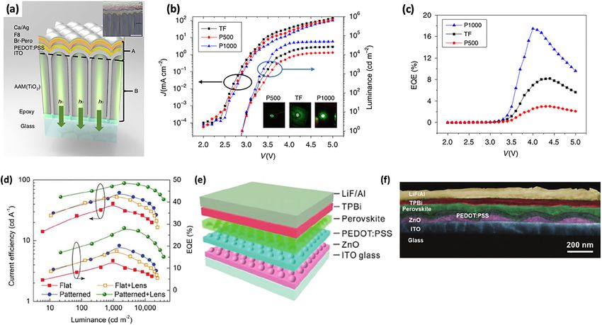
S. Kar et al.: Light management for high-performance perovskite LEDs          2111

                                                                                        Figure 3: Number of PR events N in a
                                                                                        CsPbBr3-based PeLED as a function of
                                                                                        (a) film thickness (for an applied voltage
                                                                                        giving 1000 lm m−2 with no charge
                                                                                        trapping), (b) voltage for different charge
                                                                                        trapping rates. (c) (N on log scale) as a
                                                                                        function of front transmission and back
                                                                                        reflection coefficients. (d) Normalized
                                                                                        photoluminescence spectra for direct,
                                                                                        randomized and maximal emittance
                                                                                        models. (e) N and luminous emittance as
                                                                                        functions of applied voltage for the three
                                                                                        models for emission into a full 2π
                                                                                        hemisphere and (f) into a 2.5° cone about
                                                                                        the surface normal. Reproduced with
                                                                                        permission from [172]. (g) Predicted spatial
                                                                                        photocurrent decay for perovskite thin film
                                                                                        with and without PR. (h) External PLQYs for
                                                                                        MAPbI3−xClx for different substrates. (i)
                                                                                        Experimentally measured light emission
                                                                                        map for different separation distances
                                                                                        between collection and excitation.
                                                                                        Reproduced with permission from [168] and
                                                                                        [173].

PLQY. By correlating data from transient absorption (TA)        films of 2D-3D PEA2Csn−1PbnBr3n+1 perovskite are used to
and PLQY, the monomolecular non-radiative recombination         distinctly trace scattered photons versus recycled photons
has been traditionally attributed to trap-mediated SRH          at a finite distance from the excitation point by marking the
pathways whereas the radiative bimolecular recombination        corresponding redshifts [151]. Through this, PR was shown
was shown to originate from band-to-band transitions [176].     to account for 55% of the total luminance intensity.
With the three-particle non-radiative Auger processes           Localized excitation giving rise to light output at a distance
forming the other major loss mechanism, the carrier             was also observed when further applied to a PeLED, which
recombination landscape in such systems has been well-          reinforces the proposed dependence of PR on device
explored. PR affects the radiative bimolecular constant as      geometry (lateral and vertical). On a slightly different note,
apparent through the higher internal recombination con-         optically thick MAPbX3 bulk single crystals were studied,
stant being up to 8 times higher than the externally observed   and their significant PL redshift as compared to their thin-
constant [173]. Richter et al. show that, with an escape        film counterparts was attributed to PR events [178]. It was
probability of ∼12.5%, 7 out of 8 photons in a MAPbX3 (X = I,   also shown that the dependence of PL peak energy on the
Br)-based LEDs will undergo recycling to produce a 20%          grain size in polycrystalline thin films is explainable by
external PLQE. Without re-emission processes, this value        considering intra- and inter-grain PR events along with the
would have been a mere ∼9%.                                     spatial distribution of excited carriers.
    Several works on these lines have ventured to experi-            In summarizing these various findings, some key
mentally materialize such theoretical predictions. By           points emerge that are seen to be valid for all cases. First,
modifying critical experimental parameters, the maximum         maximizing the emittance seems to be the key route to
EQE limit can be escalated to lie between 30 and 50% [177].     achieving high-performing LEDs. This is irrespective of the
Overall, the common aim is to fabricate devices with opti-      amount of PR events in the system. Second, it is critical to
mally low perovskite refractive index, increased PR events      account for all optical events in the system including
and suppressed parasitic absorption through judicious           scattering, total internal reflections, reabsorption, emis-
selection of proximal transport layers and conductive           sion and all other unregulated propagation modes before
electrodes. A recent, notable report in this direction is one   and after PR events that arise due to the optical and
by Cho and co-workers, where highly luminescent thin            morphological properties of the perovskite emitter as well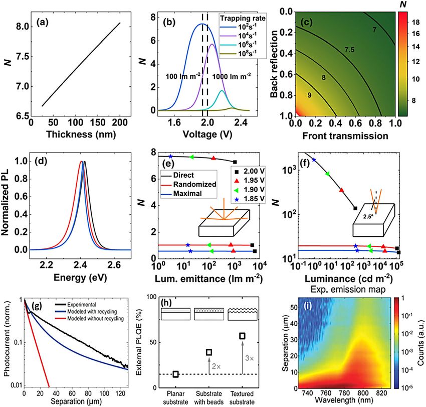
2112        S. Kar et al.: Light management for high-performance perovskite LEDs

as the device configuration. This would also include ac-            refractive index to reduce both parasitic absorption loss
curate attribution of the observed Stokes shift to PR or other      and wave-guiding effect are needed. By scanning a range of
phenomena as well as the ability to spatially and angularly         possible ETL/HTL materials (with appropriately chosen RI)
resolve emission dependencies. Third, attaining EQEs                such as ZnO/NPD, TPBi/PVK and ZnO/TFB, it was pro-
approaching almost 100% appears well within reach via               posed that the most optimum device structure for best ηout
careful device engineering, as proposed by recent reports           would consist of the following architecture: transparent
[174]. This mainly involves removing parasitic absorption           electrode/high RI transport layer/perovskite/low RI trans-
pathways through techniques such as reduction of effec-             port layer/reflective electrode [181].
tive injection area and reduction of emissive area in contact            In addition, optical nanostructures can be deployed to
with substrate. Also, as evident from applying the Moss             improve the ηout. Theoretical studies by Meng et al. corre-
relation [179], perovskite materials show dependence of             lated key parameters such as refractive indices (RI), layer
bandgap on refractive index (RI) which results in a large           thicknesses and emitter dipole orientation of materials
mismatch while outcoupled to far-field modes in air, thus            with the ηout (Figure 4c–h) [181]. The value of perovskite
inhibiting emission efficiency. This can be tackled either           refractive index varies depending on the choice of cations
through introduction of an index gradient to increase the           and halide anions as well as emission wavelength. Hence,
light escape angle or by nanostructuring. For the purpose           optical simulation is needed to design nanostructures with
of better optical management, commonly used approaches              optimal ηout. The optical losses arising from this RI
are texturing or patterning of the substrate (Figure 4a–b),         mismatch affecting the ηout can be modelled through
emitter film surface and electrodes, addition of back-               various approaches, such as transfer matrices, Monte Carlo
reflectors [182], and use of nanostructures such as micro-           and finite difference time domain methods (enabled by
lens arrays [183] to suppress stray internal reflection,             commercial software packages like MATLAB, Lumerical or
among others (as reinforced by the simulation results in            open-source platforms like Python MEEP). Meng et al.
Figure 3g–i). Further, it is possible to tune emission spec-        proposed that substrates patterned with moth-eye nano-
trally and angularly by using photonic cavities and nano-           structures with horizontal orientation of the perovskite’s
structures in conjunction with the rest of the device               transition dipole moment would be the most optimum for
architecture [184], which will be discussed in subsequent           maximizing ηout.
sections.                                                                The same report also contains another simulation
                                                                    study done for perovskite emitters in the vicinity of optical
                                                                    nanostructures affected by resonance enhancement phe-
2.2 Photon management through materials                             nomena such as Purcell effect and other wave-guiding
    and interfaces engineering                                      routes [181]. It was shown that patterned LEDs can achieve
                                                                    ηout values of 17.9, 24.8 and 38.3% respectively for blue,
In PeLEDs, taking PR into consideration and assuming                green and red, well over 1.75 times that of their planar
near unity value of EQE, the EQE can be described as [174]:         counterparts. Apart from this, there has been a steady rise
                                                                    in the number of theoretical reports in this area [186], firmly
             EQEPR, max = LEE0 /(LEE0 + Apara )              (6)
                                                                    establishing the benefit of employing such nanostructures
where LEE0 is direct light outcoupling and Apara is parasitic       for synergistic manipulation in PeLED device stacks.
absorption loss. Hence, it establishes the non-negligible           Recently, Zhang and co-workers provided a comprehensive
role played by parasitic absorption in device performance.          review on extending the ηout maximization strategies used
Furthermore, the interplay between refractive index (RI) of         in related disciplines such as organic LEDs or other con-
emitter and its surrounding too play an important role.             ventional semiconductors to perovskites [134].
Depending on the refractive index of the material sets,                  Several nanophotonic schemes including nano-
wave-guiding effect can occur, in which light is trapped            structuring the interface as well as precise nanofabrication,
inside the emitter due to the large difference in refractive        which have been employed for traditional semiconductors,
index between the active layer and its surroundings [185].          e.g. III-nitride-based LEDs [187, 188] can be transferred to
Since contacts and interfaces facilitate such losses, careful       PeLEDs as well. A broad overview of these approaches is
selection of electron-transporting layer (ETL) and hole-            illustrated in Figure 5. From bottom-up materials approach
transporting layer (HTL) are needed from both electronic            (for fabrication of nanorods, nanowires, etc.) to application
and optical point of view. While efficiency and balance of           of advanced lithographic nanofabrication techniques,
carrier injection to the emitter are considered from an             much progress has been made to achieve complete control
electronic perspective, ETL/HTL pairs with optimum                  over light propagation within the device. Taking cues from
S. Kar et al.: Light management for high-performance perovskite LEDs 2113
Figure 4: (a) Comparative study of outcoupling efficiency for planar and patterned devices: schematic of light extraction in typical planar and
textured active layers. Reproduced with permission from [180]. (b) Current density–voltage (J–V) and luminance–voltage (L–V) characteristics
for CsPbBr3 PeLEDs. Reproduced with permission from [70]. Simulated ηout of planar PeLEDs emitting at 520 nm vs. the layer thickness of ETL
and HTL with (c) low-index ETL and high-index HTL and (d) high-index ETL and low-index HTL, high-index and low-index refer to the values of 2.5
and 1.5 respectively. Normalized cross-section near-field intensity distributions of PeLEDs without and with the moth-eye nanopatterns for
light extraction in (e) planar and (f) patterned device structures emitting at 620 nm. Fractions of mode powers of (g) planar and (h) patterned
PeLEDs with an isotropic dipole orientation as a function of dipole-emitting wavelength calculated by the FDTD method. The theoretical
maximums of red (620 nm, circle), green (520 nm, star) and blue (480 nm, triangle) emitted powers into air are marked. Reproduced with
permission from [181].
these related domains, PeLEDs have also been coupled efficiency [190]. This is done by making use of plasmon
with such structures with promising results. A study using enhancement [191] and core–shell-like effects on the
vertical MAPbI3 NW arrays fabricated on porous alumina emitter [192]. One such recent work involving the incor-
membranes (PAMs) reported 45% PLQY and 130 times in- poration of Au nanospheres in the HTL of a MAPbBr3-based
crease in EQE by tuning the NW diameter [189]. About perovskite reported relative EQE enhancement of over
56-fold enhancement in IQE enabled by 2–3 times increase 50% [193]. Similarly, Ag nanorods, when introduced into
in light-outcoupling was observed when NW dimensions the perovskite–HTL interface of a CsPbBr3 system-based
were shrunk to the quantum confined regime (∼6 nm LED enabled a 43.3% improvement in EQE [194]. Yet
across). another approach has focused on nanocrystal hetero-
Apart from this, there have been instances of resonant structures with core–shell, nanocomposite, nanohybrid
nanostructures incorporation into the emitter layer, and other configurations. To this avail, systems such as
transport layer or emitter–transport interface to maximize CsPbI3-PbSe nanocomposite [195], CsPbBr3/amorphous2114 S. Kar et al.: Light management for high-performance perovskite LEDs
Figure 5: Overview of approaches to
nanostructuring the perovskite, interface or
substrate to boost emission efficiency
beyond material limits.
CsPbBrx core-shell [196], CsPbX3-ZnS heterodimers [197] near 100% EQE. This is owing to the inherent scattering and
and CsPbBr3–Ti3C2Tx MXene nanocomposites [198] have plasmonic effects of such structures coupled with heightened
been successfully demonstrated to be effective. PR events due to nanostructuring. Apart from this, device
stacks fitted with 1D metallic nanogrids (as polarizers), angle-
resolving microstructures (for directional emission) and
2.3 Deploying external outcouplers distributed Bragg reflectors (DBRs) (for narrow emission
profile), were shown to serve different purposes. These are all
The resonant light recycling in external photonic cavities feasible integrable designs for PeLEDs in the imminent future.
such as Bragg mirrors and gratings has already been shown to Tang et al. employed a moth-eye nanostructured ZnO
be useful for light extraction in several perovskite optoelec- layer in a PeLED stack to serve the dual purpose of a hole
tronic applications including photovoltaics and lasing. Shen injection layer as well as for enhanced outcoupling [70]. Lova
and co-workers fabricated PeLEDs by embedding a moth-eye and co-workers tuned the spontaneous broadband emission
nanostructure (MEN) at the front electrode/perovskite inter- of 2D (EDBE)PbCl4 perovskite by embedding it in flexible
face via soft imprinting [70]. The MEN-modified CsPbBr3 polymer DBRs [199]. This allowed directional and spectral
emitter showed massive improvement in EQE up to 20.3% redistribution of the PL for promising application in low-cost,
and current efficiency of 61.9 cdA−1, both ∼1.5 times higher large-area, lightweight flexible LEDs. Zhang chose the
from the non-nanostructured reference device. Further, they MAPbBr3 perovskite system in conjugation with anodic
showed that by employing a half-ball lens to outcoupled alumina membranes (AAM) with different nanostructure ge-
substrate-trapped photonic modes, EQE can be boosted to ometries for PeLEDs (Figure 6a–d) [200]. The AAMs served as
28.2% and CE to 88.7 cd A−1, both record values for PeLEDs three-dimensional nanophotonic substrates with a layer of
emitting in this wavelength range. Deschler et al. proposed alumina nanodome array light outcouplers and a layer of TiO2
improvised device architectures to maximize PR effect in nanowire array optical antennae. This enabled an EQE
PeLEDs [174]. Reduced contact area of nanostructured elec- enhancement from 8.19 to 17.5% for the champion device of
trodes (S. Kar et al.: Light management for high-performance perovskite LEDs 2115
extraction efficiencies reach ∼73.6% in these device archi- highly reflective HfO2/SiO2 planar dielectric layers forming
tectures due to both enhancement of emission and its spatial DBRs as the optical resonator for a vertical cavity surface-
confinement within the photonic structure. Along similar emitting laser (VCSEL) with a perovskite emitter [203]. A
lines, the aforementioned abrupt difference in refractive in- high cavity Q-factor was attained in this configuration
dex between perovskite and air was bridged by another report which was later extended to flexible polymer substrates.
that demonstrated a 14.6% EQE in MAPbI3-based red/NIR With significant stability and lasing lifetime, such nano-
LEDs employing a randomly distributed nanohole array structured DBR stacks are also promising candidates for
embedded in a SiN layer between the anode and substrate PeLEDs. Finally, it is essential to note that technological
[201]. The SiN layer and the nanohole array with RI values of transfer from the domain of organic, inorganic and
2.02 and 1.0 respectively, enable much higher light extrac- polymer-based conventional semiconductor LEDs that
tion, up to 1.64 times the planar control device. heavily employ nanostructures, would be extremely
In a novel approach to combine the abovementioned beneficial for PeLEDs.
techniques, Geng et al. demonstrated a hybrid plasmonic- Yet another exciting application of halide perovskites
photonic architecture to amplify the emission and create has been seen in the field of active metadevices [190, 204].
directionality through a hybrid metal-dielectric system Moving away from traditional plasmonics or photonics-
[202]. One-dimensional DBRs fabricated by alternate layers enabled spatial confinement at the nanoscale, metaoptics
of SiO2 and ZrO2 were used in conjunction with GdVO4:Eu3+ seeks to solely utilize optically resonant dielectric nano-
nanophosphor emitters to generate field enhancement structures for this purpose. To overcome low quantum
through Tamm plasmons. The hybrid character of this yields and fabrication-related challenges in traditional
stack was shown to exhibit reduced dissipative modes and semiconductors, halide perovskites seem to offer a prom-
efficient outcoupling of trapped electromagnetic energy to ising alternative. It has been shown in several theoretical
free-space radiative modes. Such approaches seem to be studies that strong light confinement in such nano-
extremely promising for application in PeLEDs as well in structures result in better light–matter interaction and in
the near future. On similar lines, Chen and co-workers used turn, enhances light emission from the emitter material
Figure 6: Devices on nanophotonic substrate (a) Device schematic. The materials from top to bottom are: Ca/Ag electrode, F8, CH3NH3PbBr3
(Br-Pero), PEDOT: PSS, ITO and anodic alumina membrane (AAM). AAM channels are filled with TiO2. Device performance. (b) J–V curve,
luminance and (c) external quantum efficiency (EQE) of the thin film (TF) and AAM samples. Reproduced with permission from [200]. (d) EQE
and CE vs. luminance for device with and without patterning for comparison. (e) Schematic of device with patterned substrate of configuration
glass/ITO/ZnO/PEDOT:PSS/CsPbBr3/TPBi/LiF/Al and (f) cross-sectional SEM. Reproduced with permission from [70].2116 S. Kar et al.: Light management for high-performance perovskite LEDs
[205]. These devices are inspired by high RI, dielectric medium, and unwanted Auger recombination losses etc.
metamaterials, where the electromagnetic response is that commonly occur in perovskite-based devices. Most of
attributed to the magnetic dipole resonances and optical these obstacles have been outlined in detail recently by
magnetism, arising from resonant dielectric nano- Rand et al. [211] and Gao et al. [212]. It is thus imperative to
structures. The fundamental idea is to use sub-micrometre probe further into improving the thermodynamic stability
Mie atoms (Mie-resonant nanoparticles) to create optical of such systems. In the next section, we will discuss the
metasurfaces with tuneable functionalities [204]. As origin, underlying photophysics and possible solutions to
applied to perovskite materials, high RI and facile geo- stability challenges that plague PeLEDs currently.
metric tuneability enable strong geometric resonances and
electromagnetic interferences between the multipolar
modes corresponding to the constituent elements of the 3 Defects and their effect on
structure. Such metaoptical structures in the form of
spheroids, disks, cuboids (for instance, as nanocrystals) perovskite stability
have been realized and used for many successful applica-
tions [132]. 3.1 Defects and spatial heterogeneities in
Beyond PeLED, perovskites have also been demon- perovskites
strated to be superior gain mediums for lasing applications
owing to their lower amplified stimulated emission (ASE) Fabrication of films from solution-based processing,
threshold (an order of magnitude lower than commercially though ideal for implementation in low-cost, large-scale
established systems such as ZnSe, CdS, organic semi- manufacturing (roll-to-roll processing), often suffer from
conductors etc.) [206]. Nanostructured optical cavities, rapid formation of defects during their preparation [213]
when used as high-quality feedback resonators, provide a (Figure 8a). According to previous calculation and exper-
promising route to achieve lasing in these material sys- imental results [108, 217–219], the nature and density of
tems. With careful tuning of key parameters such as the defect states in perovskites is highly sensitive to the film
spectral linewidth, efficiency of outcoupling for generated deposition conditions [220]. Point defects, which include
light, cavity Q-factor, gain coefficient and lasing threshold, vacancies, interstitials and antisites, dominate in perov-
efficient perovskite lasers can be attained. Along with skites, with the propensity of their formation highly
nanoengineering the feedback structure, many reports also dependent on the formation energy—where lower forma-
point towards the advantage of nanostructuring the gain tion energy translates to these defects forming more readily
medium itself [207]. (Figure 8b). Thankfully, for perovskites, the low formation
For cavity effects, periodic optical nanostructures such energy of shallow defects means that these are more ther-
as gratings and mirrors have been frequently used. To modynamically favoured [108, 218] as compared to the
attain strong photon confinement, high reflectivity, uni- deep defects, which are more detrimental to its intrinsic
directionality and low-loss wave-guiding of propagating properties. Though less destructive in nature, shallow de-
modes, several architectures such as distributed Bragg fects are not only sites for non-radiative recombination, but
reflectors [202], Fabry–Perot resonators, periodic gratings, also present a pathway for degradation such as vacancy-
whispering gallery mode (WGM) cavities [209] etc. have mediated ion migration and/or environment stressor-
been reported to exploit optical phenomena such as Purcell facilitated degradation (Figure 8c). The susceptibility of
effect, multiple reflections, wavelength-specific scattering, perovskite to ambient related degradation during film
polaritonic behaviour etc. for amplification of emission preparation and device operation calls attention to the
(Figure 7). Recently, optically pumped lasing has been need to address these defects in order to mitigate issues in
shown to be possible in an LED device architecture with perovskite stability. Comprehensive reviews on defect for-
embedded resonator [210]. Such advancements appear to mation mechanisms in perovskites and their impact on
be extremely promising for imminently possible deploy- optoelectronic devices have previously been published by
ment of perovskite systems in lasing applications. Chen et al. [221]. These localized degradation regions act as
It is important to note that the primary impediments to points for initialization of device failure, with the dead
further advancement are several fundamental challenges regions becoming paths of least resistance, leading to
that demand extensive investigation into the material consequences such as spectral intermittency or blinking in
system itself. These include poor operational stabilities at emission [222]. Single nanoemitters with strong quantum
high injection density, substantial Joule heating, imbal- confinement such as semiconductor quantum dots, on the
anced charge injection, local electric fields in the gain other hand, have traditionally been shown to exhibitS. Kar et al.: Light management for high-performance perovskite LEDs 2117 Figure 7: (a) Different forms of photonic cavities (mirrors, microresonators, micro-Bragg stacks, photonic crystals) and plasmonic cavities (trapped standing wave-type SPP cavities, collapsed structures with localized modes, dipole nanoantenna and coupled gap plasmon system respectively). (b) Schematic indicating the various energy dissipation pathways for an excited emitter with dipole moment (μ) in a plasmonic cavity mode (E). (c) Graphic illustrating the increase of brightness of a quantum emitter from the uncoupled free-space value to the theoretical maximum when coupled to a plasmonic nanocavity, given a saturated pumping regime. Here, η0 is the emitter quantum efficiency, ηcav is the radiation efficiency of the cavity, Γ0 the spontaneous emission rate of the uncoupled molecule, and κ the total cavity decay rate. (d) A cavity provides a frequency-specific way to locally increase the density of states. By placing an emitter in a cavity resonant to its emission, the rate, with which it emits can be considerably enhanced. (e) Map showing coupling strength as a nanoantenna is scanned over an excited single fluorescent molecule at a particular height separation extracted using lifetime values recorded at each point using time-correlated single photon counting. Reprinted with permission from [208]. Copyright (2018) American Chemical Society. (f) SEM image and schematic illustration of an embedded dielectric/metal heterostructure for the plasmonic output of a dielectric laser. (g) Schematic illustration of localized surface plasmon resonance (LSPR) enhancement mechanisms in metal-halide perovskites utilizing a plasmonic cavity: far-field scattering, near-field coupling, hot-electron transfer and plasmon resonant energy transfer. Reproduced with permission from [132]. spatially heterogeneous blinking [223]. In perovskite ensemble. Therefore, for emitters with dimensions greater nanocrystals (NCs), this has been attributed to long-lived than the quantum confinement range, homogeneous in- carrier trapping in surface defects or intermittent Auger tensity of PL is observed under moderate excitation flu- recombination processes leading to charging–discharging ences. The only instances where spectral correlation cycles of the emissive NC [224]. More interestingly, this between individual emitters in an extended system have behaviour which was previously perceived to be valid only been observed are in CdSe quantum wires and individually for nanoscale emitters, has recently been shown for mi- stacked monolayers of MoSe2/WS2 (transition metal crocrystals beyond the diffraction limit [221]. In general, dichalcogenides), both of which are attributed to delo- constituent emitters spread over distant domains, are calized excitons facilitating unprecedented charge trans- spatiotemporally uncorrelated and average out over the port [225, 226]. However, in a recent work, Pathoor et al.
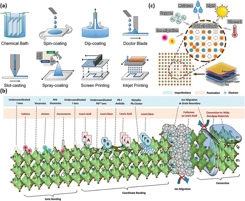
2118          S. Kar et al.: Light management for high-performance perovskite LEDs

Figure 8: Schematic on the (a) various types of solution-based processing techniques with applicability to perovskites. Adapted with
permission from [214]. (b) Types of defects present in perovskites and passivation routes to mediate them. Adapted with permission from
[215]. (c) Mediation of perovskite degradation by crystal lattice defects. Adapted with permission from [216].

demonstrated spatial synchronicity in the fluorescence                 morphological heterogeneity at sub-grain (10 µm) (Figure 9e) [233]. Experimentally, several groups
towards mesoscale carrier migration, aided by the pres-               have attempted to correlate in operando and ex situ mea-
ence of metastable trap states as the possible mechanism              surements via spectroscopic studies in a bid to explain
for such behaviour [227].                                             the degradation processes characterizing these systems. For
     Aside from crystal lattice defects, poor homogeneity of          instance, Andaji-Garmaroudi et al. studied the degrada-
perovskite morphology, can also be equally destructive.               tion of (Cs0.06FA0.79 MA0.15)Pb(I0.85Br0.15)3-based PeLEDs
Wide variation in grain size and/or film uniformity arising           through simultaneous, nanoscale, cross-sectional chemical
from poor wetting critically affects the luminous efficacy            mapping (STEM-EDX and PES) using transient and steady-
and lifetimes across individual grains in the system, mani-           state spectroscopic measurements [234]. The heterogeneity
festing in the form of low device efficiency and unidentified         at play here was found to be the accumulation of bromide
loss pathways [228]. Some of these degradation routes are             ions at one interface leading to charge injection imbalance
elucidated in Figure 9a–d.Many studies on defect tolerance            and non-radiative recombination losses. Passivation with
properties of perovskites have shown the existence of                 potassium was shown to immobilize the halide and boost
You can also read