Graphene Interface Engineering for Perovskite Solar Modules: 12.6% Power Conversion Efficiency over 50 cm2 Active Area - General Graphene Corp
←
→
Page content transcription
If your browser does not render page correctly, please read the page content below
Letter
http://pubs.acs.org/journal/aelccp
Graphene Interface Engineering for Perovskite
Solar Modules: 12.6% Power Conversion
Efficiency over 50 cm2 Active Area
Antonio Agresti,§ Sara Pescetelli,§ Alessandro L. Palma,§ Antonio E. Del Rio Castillo,‡
Dimitrios Konios,∥ George Kakavelakis,∥ Stefano Razza,§ Lucio Cinà,§ Emmanuel Kymakis,∥
Francesco Bonaccorso,*,‡ and Aldo Di Carlo*,§
See https://pubs.acs.org/sharingguidelines for options on how to legitimately share published articles.
§
C.H.O.S.E. (Centre for Hybrid and Organic Solar Energy), Department of Electronic Engineering, University of Rome Tor Vergata,
via del Politecnico 1, 00133 Rome, Italy
‡
Istituto Italiano di Tecnologia, Graphene Labs, Via Morego 30, 16163 Genova, Italy
∥
Center of Materials Technology and Photonics & Electrical Engineering Department School of Applied Technology, Technological
Downloaded via DURHAM UNIV on July 25, 2018 at 06:23:25 (UTC).
Educational Institute (T.E.I) of Crete Heraklion, 71 004 Crete, Greece
*
S Supporting Information
ABSTRACT: Interfaces between perovskite solar cell (PSC) layer
components play a pivotal role in obtaining high-performance
premium cells and large-area modules. Graphene and related two-
dimensional materials (GRMs) can be used to “on-demand” tune
the interface properties of PSCs. We successfully used GRMs to
realize large-area (active area 50.6 cm2) perovskite-based solar
modules (PSMs), achieving a record high power conversion
efficiency of 12.6%. We on-demand modulated the photoelectrode
charge dynamic by doping the mesoporous TiO2 (mTiO2) layer
with graphene flakes. Moreover, we exploited lithium-neutralized
graphene oxide flakes as interlayer at the mTiO2/perovskite
interface to improve charge injection. Notably, prolonged aging
tests have shown the long-term stability for both small- and large-
area devices using graphene-doped mTiO2. Furthermore, the possibility of producing and processing GRMs in the form of
inks opens a promising route for further scale-up and stabilization of the PSM, the gateway for the commercialization of
this technology.
in spin-coating the perovskite layer by using a mixture of γ-
T he recent development of perovskite solar cell (PSC)
technology gave rise to an unprecedented power
conversion efficiency (PCE) improvement from η =
3.8%1 up to 22.1%2 in less than 7 years. The demonstrated PCE
values make the PSC technology competitive with second-
butyrolactone (GBL) and dimethyl sulfoxide (DMSO) as the
main solvents, followed by a toluene or chlorobenzene (used as
antisolvents) treatments during the spinning process.15−18
However, although uniform and pinhole-free perovskite layers
generation thin-film photovoltaics such as copper indium are produced, this approach is hardly scalable to large and
gallium selenide (CIGS) or cadmium telluride (CdTe).3 The module size substrates because of the difficulty in uniformly
PSC success is strictly linked with the remarkable efforts made depositing by spin coating the antisolvent on large-area
to improve the device’s structure, to fine control the growth
substrates. To overcome such limitations, several alternative
and the morphology of the active perovskite layer, and to
techniques for the perovskite deposition have been proposed,19
engineer the interfaces between the cell’s constituent layers.4−10
The PCE record of PSCs11 has been achieved with the with the solution-process methods being the most promising
archetypal mesoscopic device configuration using n-type ones, e.g., enabling cost-effective20,21 roll-to-roll production.22
mesoporous TiO2 (mTiO2) layer as electron transport layer In particular, the one-step deposition allows a pinhole-free
(ETL).12,13 For this structure,11 a mixture of formamidinium perovskite deposition directly on compact TiO2 layer (cTiO2),
and methylammonium as the monovalent cations with the
addition of inorganic cesium has been used to grow perovskite Received: December 9, 2016
crystals, with the layer morphology finely controlled by Accepted: December 27, 2016
exploiting a solvent-engineering technique.14 The latter consists Published: December 27, 2016
© 2016 American Chemical Society 279 DOI: 10.1021/acsenergylett.6b00672
ACS Energy Lett. 2017, 2, 279−287
ACS Energy Letters                                                                                                                          Letter

Figure 1. Structures of small-area PSCs: (a) PSC-A with the reference mesoscopic structure FTO/cTiO2/mTiO2/perovskite/spiro-OMeTAD/
Au, (b) PSC-B with GO-Li as interlayer between perovskite and mTiO2, (c) PSC-C using graphene-doped mTiO2 layer, and (d) combined
PSC-D structure FTO/cTiO2/G+mTiO2/GO-Li/perovskite/spiro-OMeTAD/Au.

in the so-called planar configuration, leading to the most                    treatment of the mTiO2 layer prior to the perovskite
efficient fabrication procedure (i.e., PCE approaching 18%).23                 deposition32,50 and/or TiO2 doping,51,52 (ii) the use of different
However, planar PSCs usually suffer from large current−voltage                TiO2 nanostructures53−55 and heterostructures,56 and (iii) the
(I−V) hysteresis phenomena.24−26 The insertion of a mTiO2                    modification of energy levels by the addition of interface
scaffold25 combined with a two-step perovskite deposition,27                  layers.57−59 Moreover, the potential to tune the perovskite/
with the deposition of PbI2 layer prior to dipping the substrate             mTiO2 interface60 allows the reduction of the I−V curve
in a methylammonium iodide (MAI)−2-propanol (IPA)                            hysteresis,61 while at the same time improving the charge
solution,28−30 reduces the I−V hysteresis.25 In fact, the                    collection at the PE.32
presence of mesoporous metal oxide scaffolds such as Al2O331                     Graphene and related two-dimensional (2D) materials
or TiO232 aids the perovskite crystal formation, hindering short             (GRMs) are emerging as the paradigm shift of interface
circuit between photo (PE) and counter (CE) electrodes.25,33                 engineering to boost both photovoltaic performance19,62,63 and
The two-step procedure is the preferred perovskite deposition                stability of PSCs.58,64 In fact, owing to their 2D nature and the
method for large-area mesoscopic PSCs and perovskite-based                   large variety of 2D crystals possessing complementary (opto)-
solar modules (PSMs), ensuring a deeper perovskite infiltration               electronic properties,65 which can be on-demand tuned by
into the mTiO2 scaffolds compared to the single-step process.34               chemical functionalization and edge modification,66 GRMs can
This determines a fine control of the morphology of the                       be considered ideal materials for PSC interface engineering.
perovskite capping layer over interpenetrated TiO2/perovskite                The first experiments have demonstrated the use of graphene
substrate, which is beneficial for improving the perovskite film               oxide (GO) or reduced graphene oxide (RGO) as dopants in
uniformity,35 boosting the performance of the final devices.27                transport layers67−69 and as interlayers between perovskite and
   Despite the remarkable PCE value achieved by using                        transporting layers70,71 with the aim of improving the charge
mesoscopic PSCs,36−38 record efficiency (22.1%)11 is yet far                   collection mechanism at the electrodes.72,73 Moreover, GRM-
from the predicted efficiency limit (∼31%).39 Notably, losses                  based inks can be produced by cheap and high-yield
due to interfacial recombination40 negatively affect the charge               manufacturing processes using nontoxic solvents such as
injection at perovskite/transporting layer interface. Similarly,             ethanol (EtOH) or IPA.74−76 This allows the integration of
poor charge transport in electron (ETL)41 and hole (HTL)42,43                GRMs in an in-line production process for large-area perovskite
transporting layers severely limits charge collection at the                 devices and modules, with the aim of reducing performance
electrodes. These phenomena lead to a reduction of both                      losses experienced by PSC scale-up.77,78 In fact, the scale-up
device short-circuit current (ISC) and fill factor (FF),44−46 thus            process amplifies typical problems79 undergone in perovskite
reducing the PCE. Among the recently identified recombina-                    films deposition such as nanoscale pinholes,80 crystal grain
tion mechanisms for methylammonium lead triiodide (MAPI)                     boundaries,81 and perovskite film roughness,82 which can
based PSCs,47 those involving TiO2/MAPI and MAPI/hole                        severely affect the film quality and consequently the module
transport material (HTM) interfaces play a crucial role in                   PCE.23,83−87 The aforementioned problems have so far limited
limiting the PCE.40 In particular, (i) interfacial electron transfer         the maximum delivered power (MDP) of PSMs. The record
from the MAPI conduction band (CB) to the HTM and/or to                      PSM efficiency, i.e., PCE = 14.9%, has been achieved for an
TiO2 surface states47 and (ii) interfacial electron transfer from            active area of 4 cm2 with a MDP of 58 mW;88,89 when the
TiO2 CB to the HTM and/or to MAPI need to be                                 active area is increased to 60 cm2, the PCE reduces to 8.7%,14
prevented.48,49 A fine-tuning of interface and interlayer                     with a MDP of 552 mW.
properties is mandatory to enhance the charge transport and                     In this work, we demonstrate that GRMs can indeed be the
extraction at the mTiO2/MAPI interface by (i) chemical                       key elements for an efficient strategy of PSC scale-up.
                                                                       280                                           DOI: 10.1021/acsenergylett.6b00672
                                                                                                                      ACS Energy Lett. 2017, 2, 279−287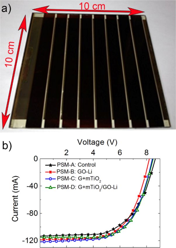
ACS Energy Letters                                                                                                                        Letter

Figure 2. Photovoltaic parameters measured at 1 SUN and relative standard deviation on 12 PSCs (open-circuit voltage, VOC; short-circuit
current density, JSC; fill factor, FF; and PCE reported in panels a, b, c, and d, respectively), for the four investigated PSCs.

Graphene interface engineering (GIE) is proposed as an                     with respect to the PSC-A, mainly due to an increase of the
effective way to boost PCE of both PSCs and PSMs by limiting                short-circuit current density (JSC), see Figure 2. In particular,
the charge losses occurring at the perovskite/mTiO2 interface,             the insertion of GO-Li, as interlayer between perovskite and
improving at the same time the stability. In particular, lithium-          mTiO2 (PSC-B), leads to a significant improvement of the
neutralized graphene oxide (GO-Li) flakes have been                         average JSC values (+18%), while a 4.3% loss in the averaged
introduced as interlayer at the mTiO2/perovskite interface72               open-circuit voltage (VOC) is observed. We do hypothesize that
with the aim of improving the charge injection from the                    the VOC reduction is linked with the presence of the GO-Li,
perovskite to the mTiO2, while graphene flakes have been                    which induces a downward displacement of the TiO 2
dispersed into the mTiO2 layer58 to speed up the charge                    conduction band (CB) with a consequent reduction of
dynamic at the PE.58 This allowed us to realize a GRMs-based               VOC72,94 (see Figure 2a). With respect to the use of graphene
PSC module having a PCE of 12.6% on an over 50 cm2 active                  flakes, the GO-Li insertion within the mesoporous layer
area and a MDP of 638 mW at 1 SUN illumination conditions.                 resulted in an increased JSC (+9.6%) compared to that of the
   Small-Area Cells. Small-area solar cells (0.1 cm2) are realized         PSC-A (Figure 2b). Contrary to the GO-Li case, the graphene
to assess the influence of GIE on PSCs with respect to the                  flakes addition does not lead to a reduction in the VOC value.
reference device (Figure 1a). We exploit graphene flakes and                Finally, the type D structure shows an overall PCE improve-
GO-Li produced by solution processing;75,90 see the Support-               ment of about 7% with respect to the reference one, which is
ing Information for both technical details and morphological               linked with an increase of 7% of the JSC value, retaining, at the
characterization. In addition, Raman characterization91−93 of              same time, satisfying VOC values when compared to that of the
graphene-based mesoscopic substrates is provided in Figure S3.             PSC-A. We point out that the reduction of the PCE standard
By using the standard two-step production procedure detailed               deviation achieved in the case of PSC-D is highly desirable for
in the Supporting Information, the small-area reference PSCs               large-area PSCs, where local inhomogeneity of the active layer
(indicated in the following as PSC-A) have shown an averaged               can affect the device’s PCE.34,95
PCE of 13.5% calculated on 12 cells. In addition, 3 PSC sets are              To gain a deeper understanding of the effect of GIE on the
realized by using the GIE strategy. In particular, in sample B             PSCs performance, electro-optical characterizations and tran-
(PSC-B), a GO-Li interlayer is spin coated onto the mTiO2                  sient measurements are carried out on encapsulated PSCs (see
layer before the perovskite deposition (Figure 1b), while in               the Supporting Information for details). The increase in JSC for
sample C (PSC-C), see Figure 1c, graphene ink is dispersed                 PSC-B and PSC-C (see Figure 2b), with respect to PSC-A, is
into the mTiO2 paste to form the graphene-doped cell scaffold               confirmed by the incident photon-to-current conversion
(G+mTiO2); see the Supporting Information for experimental                 efficiency (IPCE) spectra and by the extracted integrated JSC
details and Raman characterization (Figure S3). Finally, in                values reported in Figure S5a. In particular, the GO-Li
device D (PSC-D), the GO-Li interlayer is deposited onto the               interlayer enhances the IPCE in the spectral range between
G+mTiO2 scaffold (Figure 1d), realizing a combined structure.               400 and 600 nm, with respect to the PSC-A,72 up to a
The different PSC configurations are reported in Figure 1 (see               maximum of +7% at 440 nm (see Figure S5b). An IPCE
Figure S4 for the corresponding energy band diagram), while                increase of 8.6% is observed at ∼760 nm. The long-wavelength
the statistical photovoltaic parameters measured for each set of           IPCE rise with respect to reference PSC is more significant for
PSCs are reported in Figure 2.                                             PSC having the G+mTiO2 scaffold (PSC-B), see Figure S5b.
   The GRM-based PSCs (i.e., PSC-B, PSC-C, and PSC-D)                      This phenomenon could be linked with two different processes,
show higher PCEs (+14.8%, +13.6%, and +6.1%, respectively)                 i.e., (i) efficient electron injection from perovskite to mTiO2
                                                                     281                                           DOI: 10.1021/acsenergylett.6b00672
                                                                                                                    ACS Energy Lett. 2017, 2, 279−287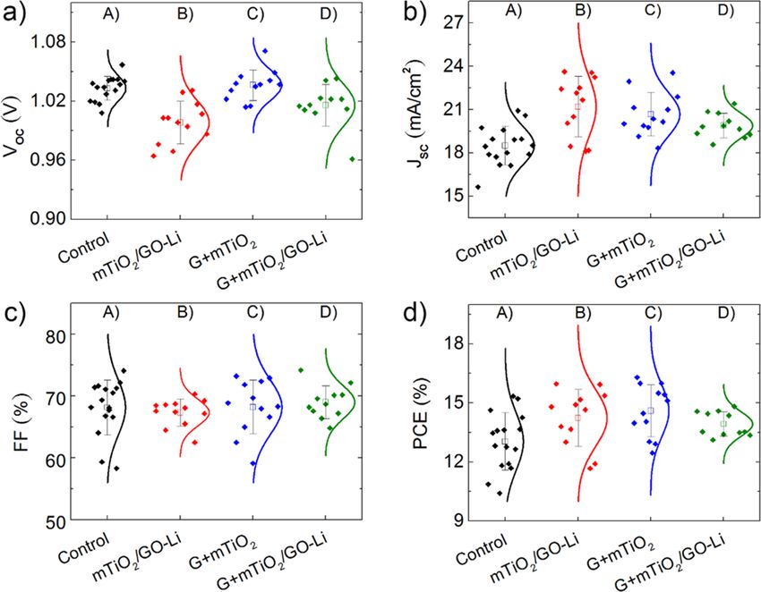
ACS Energy Letters                                                                                                                           Letter

Figure 3. (a) JSC and (b) normalized VOC rise profile acquired by retaining the tested devices in open-circuit conditions, in the dark, and by
suddenly (t = 0) switching on the light at 1 SUN irradiation conditions.

and/or (ii) increased charge transport and collection at the PE.             have been used in dye-sensitized solar cell (DSC) technology
To get an insight into the physical mechanism responsible for                and recently adopted also for PSCs.99,100 The VOC rise test is
the IPCE increase, discriminating the charge injection process               carried out by taking the device from steady-state operating
from transport and collection phenomena, we carried out                      conditions under dark at open circuit, switching on the light
transient measurements. We recorded JSC (Figure 3a) and VOC                  source, and monitoring the subsequent rise in photovoltage.101
(Figure S6a) over 3 decades of incident optical power (i.e.,                 The concentration of the photoinjected electrons in the TiO2
from 0.002 to 2 SUN) by using a white LED (see the                           film primarily determines the photovoltage transient profile.
Supporting Information for details).                                         Moreover, the buildup of electrons is in competition with the
   The JSC vs Pinc plots of Figure 3a show linear trends for all the         electron recombination processes, which is detrimental for the
investigated PSCs, an indication of energy level matching (see               device performance. As reported in Figure 3b, both PSC-B and
Figure S4) of the device component layers. In fact, a nonlinear              PSC-D show faster VOC rise profile, which can be associated
trend of JSC versus light intensity is linked with the existence of          with a better charge injection at the perovskite/mTiO2
energy barriers within the device, negatively affecting the charge            interface, with respect to the reference one. This result is
extraction process.96 Moreover, a nonlinear shape is indicative              correlated to the increase of JSC vs Pinc slope already reported in
of geminate recombination mechanism involving the hole−                      Figure 3a. Remarkably, PSC-C and PSC-D have shown the
electron exciton and/or space charge limitation at the                       fastest dynamic due to the presence of graphene flakes within
heterojunction associated with unbalanced electron and hole                  the mTiO2 layer. Thus, the obtained PCE values reported in
mobilities.97 For our PSCs, both the insertion of graphene into              Figure 2d (i.e., PCE = 16.4% for top PCE using G+mTiO2
the mTiO2 layer (PSC-C) and the GO-Li interlayer between                     layer) are linked with optimized charge injection processes.
perovskite and mTiO2 (PSC-B) led to an improvement of the                       The influence of GIE on the stability of the PSCs is assessed
electron injection at the perovskite/TiO2 interface, as                      by both prolonged illumination at maximum power point
confirmed by the increase of JSC vs Pinc slope,96 i.e., up to                 (MPP) and shelf life tests at open-circuit conditions (see
18.4% (Figure 3a), with respect to that of the reference PSC-A.              Figure.S6 and Figure.S7).
In fact, for PSC-B the slope of the linear fitting is 224 mA/W,                  Among the tested PSCs, the PSC-C and PSC-D retain ∼88%
for PSC-C 217 mA/W, and for PSC-D 225 mA/W, while for                        of the initial PCE after 16 h of endurance test, showing longer
the reference PSC-A a value of only 190 mA/W is obtained.                    lifetime with respect to the one obtained by the other types of
The optimization of charge extraction has been experimentally                PSCs. Stationary and transient electro-optical analyses, reported
demonstrated recently for both graphene flakes/perovskite58                   in Figures S6 and S8, show that PSC-C and PSC-D have a
and GO-Li/perovskite72 interfaces. In particular, Volonakis and              moderated PE degradation with respect to PSC-A, suggesting a
Giustino98 predicted, by means of first-principles calculations               reduced occurrence of trap sites and charge recombination
on graphene−CH3NH3PbI3 interfaces, that pristine graphene                    paths following the light soaking test. In contrast, the GO-Li
suppresses the octahedral tilt in the first perovskite monolayer,             interlayer dramatically affects the device’s long-term stability
leading to a nanoscale ferroelectric distortion with a permanent             because of a significant reduction of the JSC (−84% after 16.5 h
polarization. This interfacial ferroelectricity drives electron              of light soaking test at 1 SUN). Lithium atoms degrade the
extraction from the perovskite, hindering electron−hole                      perovskite layer,69,102−104 thus compromising the perovskite/
recombination,98 a phenomenon that could explain the electron                GO-Li/mTiO2 interface and, consequently, the electron
injection mechanism at the perovskite/graphene-doped mTiO2                   injection process. Notably, the combined use of graphene in
interface experimentally demonstrated in this work. Addition-                mTiO2 and GO-Li interlayer results in a considerably improved
ally, the energy level matching between GO-Li and the mTiO2                  stability with respect to the PSC-B, especially for what concerns
layer together with TiO2 trap passivation72 facilitate electron              light stress at MPP. In fact, PSC-D (Figure S6d, curve D)
injection in PSCs with a GO-Li interlayer. A detailed study of               retains more than 70% of the initial PCE after 16 h of
the VOC dependence on Pinc (see Figure S6a) further confirms                  prolonged 1 SUN stress test.
that neither graphene flakes nor GO-Li introduce trap states in                  Large-Area Modules. To test the effectiveness of our proposed
PSCs.                                                                        GIE approach, we developed large-area modules, fabricated on
   To investigate the influence of the GRM on the electron                    a 10 × 10 cm2 substrate area, consisting of eight series-
injection and collection at the PE of the devices, we tested the             connected PSCs (active area 6.32 cm2), with an overall active
dynamic performance under pulsed light conditions with                       area of 50.56 cm2. The module aperture ratio, i.e., the ratio
transient photovoltage (TPV) measurements.99 TPV tests                       between the active area and the aperture area, is approximately
                                                                       282                                            DOI: 10.1021/acsenergylett.6b00672
                                                                                                                       ACS Energy Lett. 2017, 2, 279−287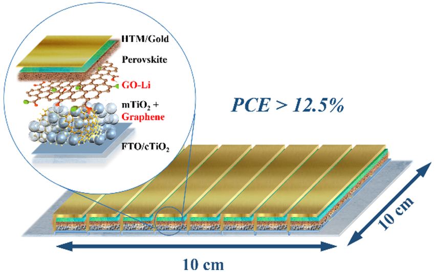
ACS Energy Letters                                                                                                                         Letter

73% (see the schematic representation of module layout                     +mTiO2 and GO-Li interlayer in PSM-D results in the most
reported in Figure S10).                                                   efficient PSM, i.e., exceeding by 9% the PCE of the reference
  The I−V characteristics of the as-produced PSMs are                      one. The as-obtained PCE values are linked with the increase of
reported in Figure 4b for each tested device structures named              FF (+8.8%), still maintaining a VOC of 8.57 V. Differently from
                                                                           the results obtained with PSCs, the PSM-D has shown the best
                                                                           PCE performance (Table 1), confirming the crucial role of GIE
                                                                           in retaining high PCE uniformity passing from small-area, i.e.,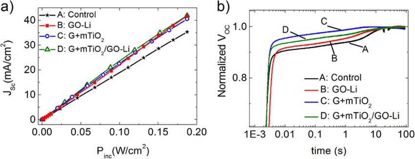
ACS Energy Letters                                                                                                                            Letter

Figure 5. Normalized (a) VOC, (b) ISC, (c) FF, and (d) PCE trends vs time extracted by 1 SUN I−V characteristics, periodically acquired
during the shelf life test (ISOS-D-1) for the four PSMs.

and GO-Li interlayer has a T80 lifetime 3 times greater than the
reference one. Moreover, the exploitation of GIE resulted in
                                                                         ■   ACKNOWLEDGMENTS
                                                                         This project has received funding from the European Union’s
prolonged shelf life stability for PSM that retained more than           Horizon 2020 research and innovation programme under grant
90% of the initial PCE after 1630 h when G+mTiO2 is used as              agreement No. 696656 − GrapheneCore1.

                                                                         ■
scaffold.
   The obtained results, coupled with both the availability of a              REFERENCES
wide library of 2D materials and the easy solution process                 (1) Kojima, A.; Teshima, K.; Shirai, Y.; Miyasaka, T. Organometal
makes interface engineering with graphene and other 2D                   Halide Perovskites as Visible-Light Sensitizers for Photovoltaic Cells. J.
materials a new design strategy for PSCs and in general for the          Am. Chem. Soc. 2009, 131, 6050−6051.
new generation of photovoltaic technologies.                               (2) Best Research-Cell Efficiencies. http://www.nrel.gov/pv/assets/

■
*
    ASSOCIATED CONTENT
S Supporting Information
                                                                         images/efficiency_chart.jpg.
                                                                           (3) Wang, B.; Xiao, X.; Chen, T. Perovskite Photovoltaics: A High-
                                                                         Efficiency Newcomer to the Solar Cell Family. Nanoscale 2014, 6,
                                                                         12287−12297.
The Supporting Information is available free of charge on the              (4) Yin, W.-J.; Yang, J.-H.; Kang, J.; Yan, Y.; Wei, S.-H. Halide
ACS Publications website at DOI: 10.1021/acsenergy-                      Perovskite Materials for Solar Cells: A Theoretical Review. J. Mater.
lett.6b00672.                                                            Chem. A 2015, 3, 8926−8942.
       Experimental details, characterization of materials (TEM,           (5) Luo, S.; Daoud, W. A. Recent Progress in Organic − Inorganic
                                                                         Halide Perovskite Solar Cells: Mechanisms and Material. J. Mater.
       AFM, SEM, Raman spectroscopy, FT-IR, XPS, UPS),                   Chem. A 2015, 3, 8992−9010.
       and spectro-electrical characterization (IPCE, I−V                  (6) Stranks, S. D.; Snaith, H. J. Metal-Halide Perovskites for
       curves, stress test) of devices (PDF)                             Photovoltaic and Light-Emitting Devices. Nat. Nanotechnol. 2015, 10,

■
                                                                         391−402.
    AUTHOR INFORMATION                                                     (7) Park, N. G. Perovskite Solar Cells: An Emerging Photovoltaic
                                                                         Technology. Mater. Today 2015, 18, 65−72.
Corresponding Authors                                                      (8) Song, T.-B.; Chen, Q.; Zhou, H.; Jiang, C.; Wang, H.-H.; Yang,
*Tel.: +39 010 71781795. E-mail: francesco.bonaccorso@iit.it.            M. Y.; Liu, Y.; You, J.; Yang, Y. Perovskite Solar Cells: Film Formation
*Tel.: +39 6 7259 7456. E-mail: aldo.dicarlo@uniroma2.it.                and Properties. J. Mater. Chem. A 2015, 3, 9032−9050.
                                                                           (9) Boix, P. P.; Nonomura, K.; Mathews, N.; Mhaisalkar, S. G.
ORCID                                                                    Current Progress and Future Perspectives for Organic/inorganic
Alessandro L. Palma: 0000-0002-1682-7032                                 Perovskite Solar Cells. Mater. Today 2014, 17, 16−23.
George Kakavelakis: 0000-0002-5395-7477                                    (10) Salim, T.; Sun, S.; Abe, Y.; Krishna, A.; Grimsdale, A. C.; Lam,
Emmanuel Kymakis: 0000-0003-0257-1192                                    Y. M. Perovskite-Based Solar Cells: Impact of Morphology and Device
Aldo Di Carlo: 0000-0001-6828-2380                                       Architecture on Device Performance. J. Mater. Chem. A 2015, 3,
                                                                         8943−8969.
Notes                                                                      (11) Saliba, M.; Matsui, T.; Seo, J.-Y.; Domanski, K.; Correa-Baena,
The authors declare no competing financial interest.                      J.-P.; Nazeeruddin, M. K.; Zakeeruddin, S. M.; Tress, W.; Abate, A.;

                                                                   284                                                 DOI: 10.1021/acsenergylett.6b00672
                                                                                                                        ACS Energy Lett. 2017, 2, 279−287
ACS Energy Letters Letter
Hagfeldt, A.; et al. Cesium-Containing Triple Cation Perovskite Solar (31) Lee, M. M.; Teuscher, J.; Miyasaka, T.; Murakami, T. N.; Snaith,
Cells: Improved Stability, Reproducibility and High Efficiency. Energy H. J. Efficient Hybrid Solar Cells Based on Meso-Superstructured
Environ. Sci. 2016, 9, 1989−1997. Organometal Halide Perovskites. Science 2012, 338, 643−647.
(12) Palma, A. L.; Cinà, L.; Busby, Y.; Marsella, A.; Agresti, A.; (32) Abdi-Jalebi, M.; Dar, M. I.; Sadhanala, A.; Senanayak, S. P.;
Pescetelli, S.; Pireaux, J.-J.; Di Carlo, A. Mesoscopic Perovskite Light Giordano, F.; Zakeeruddin, S. M.; Grätzel, M.; Friend, R. H. Impact of
Emitting Diodes. ACS Appl. Mater. Interfaces 2016, 8, 26989−26997. Mesoporous Titania-Perovskite Interface on the Performance of
(13) Palma, A. L.; Cinà, L.; Busby, Y.; Marsella, A.; Agresti, A.; Hybrid Organic-Inorganic Perovskite Solar Cells. J. Phys. Chem. Lett.
Pescetelli, S.; Pireaux, J.-J.; Carlo, A. D. Hybrid Perovskite as 2016, 7, 3264−3269.
Substituent of Indium and Gallium in Light Emitting Diodes. Phys. (33) Murugadoss, G.; Mizuta, G.; Tanaka, S.; Nishino, H.; Umeyama,
Status Solidi 2016, 13, 958−961. T.; Imahori, H.; Ito, S. Double Functions of Porous TiO2 Electrodes
(14) Seo, J.; Park, S.; Chan Kim, Y.; Jeon, N. J.; Noh, J. H.; Yoon, S. on CH3NH3PbI3 Perovskite Solar Cells: Enhancement of Perovskite
C.; Seok, S. Il Benefits of Very Thin PCBM and LiF Layers for Crystal Transformation and Prohibition of Short Circuiting. APL
Solution-Processed P−i−n Perovskite Solar Cells. Energy Environ. Sci. Mater. 2014, 2, 081511.
2014, 7, 2642−2646. (34) Matteocci, F.; Cinà, L.; Di Giacomo, F.; Razza, S.; Palma, A. L.;
(15) Jeon, N. J.; Noh, J. H.; Kim, Y. C.; Yang, W. S.; Ryu, S.; Seok, S. Guidobaldi, A.; D’Epifanio, A.; Licoccia, S.; Brown, T. M.; Reale, A.;
Il. Solvent Engineering for High-Performance Inorganic-Organic et al. High Efficiency Photovoltaic Module Based on Mesoscopic
Hybrid Perovskite Solar Cells. Nat. Mater. 2014, 13, 897−903. Organometal Halide Perovskite. Prog. Photovoltaics 2016, 24, 436−
(16) Cohen, B.-E.; Etgar, L. Parameters That Control and Influence 455.
the Organo-Metal Halide Perovskite Crystallization and Morphology. (35) Matteocci, F.; Busby, Y.; Pireaux, J.-J.; Divitini, G.; Cacovich, S.;
Front. Optoelectron 2016, 9, 44−52. Ducati, C.; Di Carlo, A. Interface and Composition Analysis on
(17) Cohen, B. El; Aharon, S.; Dymshits, A.; Etgar, L. Impact of Perovskite Solar Cells. ACS Appl. Mater. Interfaces 2015, 7, 26176−
Antisolvent Treatment on Carrier Density in Efficient Hole- 26183.
Conductor-Free Perovskite-Based Solar Cells. J. Phys. Chem. C 2016, (36) Yang, W. S.; Noh, J. H.; Jeon, N. J.; Kim, Y. C.; Ryu, S.; Seo, J.;
120, 142−147. Seok, S. Il. High-Performance Photovoltaic Perovskite Layers
(18) Park, N.-G. Crystal Growth Engineering for High Efficiency Fabricated through Intramolecular Exchange. Science (Washington,
Perovskite Solar Cells. CrystEngComm 2016, 18, 5977−5985. DC, U. S.) 2015, 348, 1234−1237.
(19) Razza, S.; Castro-Hermosa, S.; Di Carlo, A.; Brown, T. M. (37) Ahn, N.; Son, D. Y.; Jang, I. H.; Kang, S. M.; Choi, M.; Park, N.
Research Update: Large-Area Deposition, Coating, Printing, and G. Highly Reproducible Perovskite Solar Cells with Average Efficiency
Processing Techniques for the Upscaling of Perovskite Solar Cell of 18.3% and Best Efficiency of 19.7% Fabricated via Lewis Base
Technology. APL Mater. 2016, 4, 091508. Adduct of Lead(II) Iodide. J. Am. Chem. Soc. 2015, 137, 8696−8699.
(20) Fakharuddin, A.; Jose, R.; Brown, T. M.; Fabregat-Santiago, F.; (38) Ke, W.; Fang, G.; Liu, Q.; Xiong, L.; Qin, P.; Tao, H.; Wang, J.;
Bisquert, J. A Perspective on the Production of Dye-Sensitized Solar Lei, H.; Li, B.; Wan, J.; et al. Low-Temperature Solution-Processed Tin
Modules. Energy Environ. Sci. 2014, 7, 3952−3981. Oxide as an Alternative Electron Transporting Layer for Efficient
(21) Casaluci, S.; Gemmi, M.; Pellegrini, V.; Di Carlo, A.; Perovskite Solar Cells. J. Am. Chem. Soc. 2015, 137, 6730−6733.
Bonaccorso, F. Graphene-Based Large Area Dye-Sensitized Solar (39) Sha, W. E. I.; Ren, X.; Chen, L.; Choy, W. C. H. The Efficiency
Cell Modules. Nanoscale 2016, 8, 5368−5378. Limit of CH3NH3PbI3 Perovskite Solar Cells. Appl. Phys. Lett. 2015,
(22) Mariani, P.; Vesce, L.; Di Carlo, A. The Role of Printing 106, 221104.
Techniques for Large-Area Dye Sensitized Solar Cells. Semicond. Sci. (40) Marin-Beloqui, J. M.; Lanzetta, L.; Palomares, E. Decreasing
Technol. 2015, 30, 104003. Charge Losses in Perovskite Solar Cells Through Mp-TiO2/MAPI
(23) Nie, W.; Tsai, H.; Asadpour, R.; Blancon, J.-C.; Neukirch, A. J.; Interface Engineering. Chem. Mater. 2016, 28, 207−213.
Gupta, G.; Crochet, J. J.; Chhowalla, M.; Tretiak, S.; Alam, M. A.; et al. (41) Hutter, E. M.; Eperon, G. E.; Stranks, S. D.; Savenije, T. J.
Solar Cells. High-Efficiency Solution-Processed Perovskite Solar Cells Charge Carriers in Planar and Meso-Structured Organic-Inorganic
with Millimeter-Scale Grains. Science 2015, 347, 522−525. Perovskites: Mobilities, Lifetimes, and Concentrations of Trap States.
(24) Sánchez, R. S.; Gonzalez-Pedro, V.; Lee, J.; Park, N.; Kang, Y. S.; J. Phys. Chem. Lett. 2015, 6, 3082−3090.
Mora-sero, I.; Bisquert, J. Slow Dynamic Processes in Lead Halide (42) Agresti, A.; Pescetelli, S.; Casaluci, S. High Efficient Perovskite
Perovskite Solar Cells. Characteristic Times and Hysteresis. J. Phys. Solar Cells by Employing Zinc-Phthalocyanine as Hole Transporting
Chem. Lett. 2014, 5, 2357−2363. Layer. In 2015 IEEE International Conference on Nanotechnology,
(25) Kim, H. S.; Park, N. G. Parameters Affecting I-V Hysteresis of Rome, Italy, July 27−30, 2015; pp 732−735. DOI: 10.1109/
CH3NH3PbI3 Perovskite Solar Cells: Effects of Perovskite Crystal Size NANO.2015.7388712.
and Mesoporous TiO2 Layer. J. Phys. Chem. Lett. 2014, 5, 2927−2934. (43) Wang, Y.; Wang, H.-Y.; Yu, M.; Fu, L.; Qin, Y.; Zhang, J.-P.; Ai,
(26) Snaith, H. J.; Abate, A.; Ball, J. M.; Eperon, G. E.; Leijtens, T.; X. Trap-Limited Charge Recombination in Intrinsic Perovskite Film
Noel, N. K.; Stranks, S. D.; Wang, J. T.-W.; Wojciechowski, K.; Zhang, and Meso-Superstructured Perovskite Solar Cells and the Passivation
W. Anomalous Hysteresis in Perovskite Solar Cells. J. Phys. Chem. Lett. Effect of Hole-Transport Material on Trap States. Phys. Chem. Chem.
2014, 5, 1511−1515. Phys. 2015, 17, 29501−29506.
(27) Yantara, N.; Sabba, D.; Yanan, F.; Kadro, J. M.; Moehl, T.; Boix, (44) Sveinbjörnsson, K.; Aitola, K.; Zhang, X.; Pazoki, M.; Hagfeldt,
P. P.; Mhaisalkar, S. G.; Grätzel, M.; Grätzel, C. Loading of A.; Boschloo, G.; Johansson, E. M. J. Probing Photocurrent
Mesosporous Titania Films by CH3NH3PbI3 Perovskite, Single Step Generation, Charge Transport, and Recombination Mechanisms in
vs Sequential Deposition. Chem. Commun. 2015, 51, 4603−4606. Mesostructured Hybrid Perovskite through Photoconductivity Meas-
(28) Burschka, J.; Pellet, N.; Moon, S.-J.; Humphry-Baker, R.; Gao, urements. J. Phys. Chem. Lett. 2015, 6, 4259−4264.
P.; Nazeeruddin, M. K.; Grätzel, M. Sequential Deposition as a Route (45) Listorti, A.; Juarez-Perez, E. J.; Frontera, C.; Roiati, V.; Garcia-
to High-Performance Perovskite-Sensitized Solar Cells. Nature 2013, Andrade, L.; Colella, S.; Rizzo, A.; Ortiz, P.; Mora-Sero, I. Effect of
499, 316−320. Mesostructured Layer upon Crystalline Properties and Device
(29) Jiang, C.; Lim, S. L.; Goh, W. P.; Wei, F. X.; Zhang, J. Performance on Perovskite Solar Cells. J. Phys. Chem. Lett. 2015, 6,
Improvement of CH3NH3PbI3 Formation for Efficient and Better 1628−1637.
Reproducible Mesoscopic Perovskite Solar Cells. ACS Appl. Mater. (46) Zhao, Y.; Nardes, A. M.; Zhu, K. Solid-State Mesostructured
Interfaces 2015, 7, 24726−24732. Perovskite CH3NH3PbI3 Solar Cells: Charge Transport, Recombina-
(30) Li, Y.; Meng, L.; Yang, Y.; Xu, G.; Hong, Z.; Chen, Q.; You, J.; tion, and Diffusion Length. J. Phys. Chem. Lett. 2014, 5, 490−494.
Li, G.; Yang, Y.; Li, Y. High-Efficiency Robust Perovskite Solar Cells (47) Marin-Beloqui, J. M.; Hernandez, J. P.; Palomares, E. Photo-
on Ultrathin Flexible Substrates. Nat. Commun. 2016, 7, 10214. Induced Charge Recombination Kinetics in MAPbI3‑xClx Perovskite-
285 DOI: 10.1021/acsenergylett.6b00672
ACS Energy Lett. 2017, 2, 279−287ACS Energy Letters Letter
like Solar Cells Using Low Band-Gap Polymers as Hole Conductors. Dimensional Crystals, and Hybrid Systems. Nanoscale 2015, 7, 4598−
Chem. Commun. 2014, 50, 14566−14569. 4810.
(48) Yin, W.; Pan, L.; Yang, T.; Liang, Y. Recent Advances in (66) Kuila, T.; Bose, S.; Mishra, A. K.; Khanra, P.; Kim, N. H.; Lee, J.
Interface Engineering for Planar Heterojunction Perovskite Solar Cells. H. Chemical Functionalization of Graphene and Its Applications. Prog.
Molecules 2016, 21, 837−855. Mater. Sci. 2012, 57, 1061−1105.
(49) Yang, G.; Tao, H.; Qin, P.; Ke, W.; Fang, G. Recent Progress on (67) Han, G. S.; Song, Y. H.; Jin, Y. U.; Lee, J. W.; Park, N. G.; Kang,
Electron Transport Layer for Efficient Perovskite Solar Cells. J. Mater. B. K.; Lee, J. K.; Cho, I. S.; Yoon, D. H.; Jung, H. S. Reduced
Chem. A 2016, 4, 3970−3990. Graphene Oxide/Mesoporous TiO2 Nanocomposite Based Perovskite
(50) Giordano, F.; Abate, A.; Correa Baena, J. P.; Baena, C.; Saliba, Solar Cells. ACS Appl. Mater. Interfaces 2015, 7, 23521−23526.
M.; Matsui, T.; Im, S. H.; Zakeeruddin, S. M.; Nazeeruddin, M. K.; (68) Umeyama, T.; Matano, D.; Baek, J.; Gupta, S.; Ito, S.;
Hagfeldt, A.; et al. Enhanced Electronic Properties in Mesoporous Subramanian, V. R.; Imahori, H. Boosting of the Performance of
TiO2 via Lithium Doping for High-Efficiency Perovskite Solar Cells. Perovskite Solar Cells through Systematic Introduction of Reduced
Nat. Commun. 2016, 7, 10379. Graphene Oxide in TiO2 Layers. Chem. Lett. 2015, 44, 1410−1412.
(51) Kim, D. H.; Han, G. S.; Seong, W. M.; Lee, J.-W.; Kim, B. J.; (69) Luo, Q.; Zhang, Y.; Liu, C.; Li, J.; Wang, N.; Lin, H. Iodide-
Park, N.-G.; Hong, K. S.; Lee, S.; Jung, H. S. Niobium Doping Effects Reduced Graphene Oxide with Dopant-Free Spiro-OMeTAD for
on TiO2 Mesoscopic Electron Transport Layer-Based Perovskite Solar Ambient Stable and High-Efficiency Perovskite Solar Cells. J. Mater.
Cells. ChemSusChem 2015, 8, 2392−2398. Chem. A 2015, 3, 15996−16004.
(52) Roose, B.; Gödel, K. C.; Pathak, S.; Sadhanala, A.; Baena, J. P. (70) Yeo, J.-S.; Kang, R.; Lee, S.; Jeon, Y.-J.; Myoung, N.; Lee, C.-L.;
C.; Wilts, B. D.; Snaith, H. J.; Wiesner, U.; Grätzel, M.; Steiner, U.; Kim, D.-Y.; Yun, J.-M.; Seo, Y.-H.; Kim, S.-S.; et al. Highly Efficient
et al. Enhanced Efficiency and Stability of Perovskite Solar Cells and Stable Planar Perovskite Solar Cells with Reduced Graphene
Through Nd-Doping of Mesostructured TiO2. Adv. Energy Mater. Oxide Nanosheets as Electrode Interlayer. Nano Energy 2015, 12, 96−
2016, 6, 1501868−1501874. 104.
(53) Kim, H.-S.; Lee, J.-W.; Yantara, N.; Boix, P. P.; Kulkarni, S. A.; (71) Wu, Z.; Bai, S.; Xiang, J.; Yuan, Z.; Yang, Y.; Cui, W.; Gao, X.;
Mhaisalkar, S.; Grätzel, M.; Park, N.-G. High Efficiency Solid-State Liu, Z.; Jin, Y.; Sun, B. Efficient Planar Heterojunction Perovskite Solar
Sensitized Solar Cell-Based on Submicrometer Rutile TiO2 Nanorod Cell Employing Graphene Oxide as Hole Conductor. Nanoscale 2014,
and CH3NH3PbI3 Perovskite Sensitizer. Nano Lett. 2013, 13, 2412− 6, 10505−10510.
2417. (72) Agresti, A.; Pescetelli, S.; Cinà, L.; Konios, D.; Kakavelakis, G.;
(54) Salazar, R.; Altomare, M.; Lee, K.; Tripathy, J.; Kirchgeorg, R.; Kymakis, E.; Carlo, A. Di. Efficiency and Stability Enhancement in
Nguyen, N. T.; Mokhtar, M.; Alshehri, A.; Al-Thabaiti, S. a.; Schmuki, Perovskite Solar Cells by Inserting Lithium-Neutralized Graphene
P. Use of Anodic TiO2 Nanotube Layers as Mesoporous Scaffolds for Oxide as Electron Transporting Layer. Adv. Funct. Mater. 2016, 26,
Fabricating CH3NH3PbI3 Perovskite-Based Solid-State Solar Cells. 2686−2694.
ChemElectroChem 2015, 2, 824−828. (73) Palma, A. L.; Cinà, L.; Pescetelli, S.; Agresti, A.; Raggio, M.;
(55) Dharani, S.; Mulmudi, H. K.; Yantara, N.; Thu Trang, P. T.; Paolesse, R.; Bonaccorso, F.; Di Carlo, A. Reduced Graphene Oxide as
Park, N. G.; Graetzel, M.; Mhaisalkar, S.; Mathews, N.; Boix, P. P. Efficient and Stable Hole Transporting Material in Mesoscopic
High Efficiency Electrospun TiO2 Nanofiber Based Hybrid Organic- Perovskite Solar Cells. Nano Energy 2016, 22, 349−360.
Inorganic Perovskite Solar Cell. Nanoscale 2014, 6, 1675−1679. (74) Capasso, A.; Del Rio Castillo, A. E.; Sun, H.; Ansaldo, A.;
(56) Mahmood, K.; Swain, B. S.; Amassian, A. Core−shell Pellegrini, V.; Bonaccorso, F. Ink-Jet Printing of Graphene for Flexible
Heterostructured Metal Oxide Arrays Enable Superior Light-Harvest- Electronics: An Environmentally-Friendly Approach. Solid State
ing and Hysteresis-Free Mesoscopic Perovskite Solar Cells. Nanoscale Commun. 2015, 224, 53−63.
2015, 7, 12812−12819. (75) Bonaccorso, F.; Bartolotta, A.; Coleman, J. N.; Backes, C. 2D-
(57) Li, B.; Chen, Y.; Liang, Z.; Gao, D.; Huang, W. Interfacial Crystal-Based Functional Inks. Adv. Mater. 2016, 28, 6136−6166.
Engineering by Using Self-Assembled Monolayer in Mesoporous (76) O’Neill, A.; Khan, U.; Nirmalraj, P. N.; Boland, J.; Coleman, J.
Perovskite Solar Cell. RSC Adv. 2015, 5, 94290−94295. N. Graphene Dispersion and Exfoliation in Low Boiling Point
(58) Agresti, A.; Pescetelli, S.; Taheri, B.; Del Rio Castillo, A. E.; Solvents. J. Phys. Chem. C 2011, 115, 5422−5428.
Cinà, L.; Bonaccorso, F.; Di Carlo, A. Graphene-Perovkite Solar Cells (77) Matteocci, F.; Razza, S.; Di Giacomo, F.; Casaluci, S.; Mincuzzi,
Exceed 18% Efficiency: A Stability Study. ChemSusChem 2016, 9, G.; Brown, T. M.; D’Epifanio, A.; Licoccia, S.; Di Carlo, A. Solid-State
2609−2619. Solar Modules Based on Mesoscopic Organometal Halide Perovskite:
(59) Ogomi, Y.; Morita, A.; Tsukamoto, S.; Saitho, T.; Shen, Q.; A Route towards the up-Scaling Process. Phys. Chem. Chem. Phys.
Toyoda, T.; Yoshino, K.; Pandey, S. S.; Ma, T.; Hayase, S. All-Solid 2014, 16, 3918−3923.
Perovskite Solar Cells with HOCO-R-NH3+I- Anchor-Group Inserted (78) Galagan, Y.; Coenen, E. W. C.; Verhees, W.; Andriessen, R.
between Porous Titania and Perovskite. J. Phys. Chem. C 2014, 118, Towards Scaling up of Perovskite Solar Cells and Modules. J. Mater.
16651−16659. Chem. A 2016, 4, 5700−5705.
(60) Shi, J.; Xu, X.; Li, D.; Meng, Q. Interfaces in Perovskite Solar (79) Ye, F.; Chen, H.; Xie, F.; Tang, W.; Yin, M.; He, J.; Bi, E.; Wang,
Cells. Small 2015, 11, 2472−2486. Y.; Yang, X.; Han, L. Soft-Cover Deposition of Scaling-up Uniform
(61) Heo, J. H.; You, M. S.; Chang, M. H.; Yin, W.; Ahn, T. K.; Lee, Perovskite Thin Films for High Cost-Performance Solar Cells. Energy
S.-J.; Sung, S.-J.; Kim, D. H.; Im, S. H. Hysteresis-Less Mesoscopic Environ. Sci. 2016, 9, 2295−2301.
CH3NH3PbI3 Perovskite Hybrid Solar Cells by Introduction of Li- (80) Zhao, Z.; Chen, X.; Wu, H.; Wu, X.; Cao, G. Probing the
Treated TiO2 Electrode. Nano Energy 2015, 15, 530−539. Photovoltage and Photocurrent in Perovskite Solar Cells with
(62) Acik, M.; Darling, S. B. Graphene in Perovskite Solar Cells: Nanoscale Resolution. Adv. Funct. Mater. 2016, 26, 3048−3058.
Device Design, Characterization and Implementation. J. Mater. Chem. (81) Ren, X.; Yang, Z.; Yang, D.; Zhang, X.; Cui, D.; Liu, Y.; Wei, Q.;
A 2016, 4, 6185−6235. Fan, H.; Liu, S. F. Modulating Crystal Grain Size and Optoelectronic
(63) Balis, N.; Stratakis, E.; Kymakis, E. Graphene and Transition Properties of Perovskite Films for Solar Cells by Reaction Temper-
Metal Dichalcogenide Nanosheets as Charge Transport Layers for ature. Nanoscale 2016, 8, 3816−3822.
Solution Processed Solar Cells. Mater. Today 2016, 19, 580. (82) Sharenko, A.; Toney, M. F. Relationships between Lead Halide
(64) Singh, E.; Nalwa, H. S. Graphene-Based Dye-Sensitized Solar Perovskite Thin-Film Fabrication, Morphology, and Performance in
Cells: A Review. Sci. Adv. Mater. 2015, 7, 1863−1912. Solar Cells. J. Am. Chem. Soc. 2016, 138, 463−470.
(65) Ferrari, A. C.; Bonaccorso, F.; Fal'ko, V.; Novoselov, K. S.; (83) Deng, Y.; Peng, E.; Shao, Y.; Xiao, Z.; Dong, Q.; Huang, J.
Roche, S.; Bøggild, P.; Borini, S.; Koppens, F.; Palermo, V.; Pugno, N.; Scalable Fabrication of Efficient Organolead Trihalide Perovskite Solar
et al. Science and Technology Roadmap for Graphene, Related Two- Cells with Doctor-Bladed. Energy Environ. Sci. 2015, 8, 1544−1550.
286 DOI: 10.1021/acsenergylett.6b00672
ACS Energy Lett. 2017, 2, 279−287ACS Energy Letters Letter
(84) Hwang, K.; Jung, Y. S.; Heo, Y. J.; Scholes, F. H.; Watkins, S. E.; (101) Barnes, P. R. F.; Miettunen, K.; Li, X.; Anderson, A. Y.; Bessho,
Subbiah, J.; Jones, D. J.; Kim, D. Y.; Vak, D. Toward Large Scale Roll- T.; Gratzel, M.; O’Regan, B. C. Interpretation of Optoelectronic
to-Roll Production of Fully Printed Perovskite Solar Cells. Adv. Mater. Transient and Charge Extraction Measurements in Dye-Sensitized
2015, 27, 1241−1247. Solar Cells. Adv. Mater. 2013, 25, 1881−1922.
(85) Jiang, C.; Hsieh, Y.; Zhao, H.; Zhou, H.; Yang, Y. Controlling (102) Hawash, Z.; Ono, L. K.; Raga, S. R.; Lee, M. V.; Qi, Y. Air-
Solid-Gas Reactions at Nanoscale for Enhanced Thin Film Exposure Induced Dopant Redistribution and Energy Level Shifts in
Morphologies and Device Performances Controlling Solid - Gas Spin-Coated Spiro-MeOTAD Films. Chem. Mater. 2015, 27, 562−569.
Reactions at Nanoscale for Enhanced Thin Film Morphologies and (103) Habisreutinger, S. N.; Leijtens, T.; Eperon, G. E.; Stranks, S.
Device Performances in Solution - Processed Cu2ZnSn (S,Se)4 Sol. J. D.; Nicholas, R. J.; Snaith, H. J. Enhanced Hole Extraction in
Am. Chem. Soc. 2015, 137, 11069−11075. Perovskite Solar Cells through Carbon Nanotubes. J. Phys. Chem. Lett.
(86) Razza, S.; Di Giacomo, F.; Matteocci, F.; Cinà, L.; Palma, A. L.; 2014, 5, 4207−4212.
Casaluci, S.; Cameron, P.; D’Epifanio, A.; Licoccia, S.; Reale, A.; et al. (104) Habisreutinger, S. N.; Leijtens, T.; Eperon, G. E.; Stranks, S.
Perovskite Solar Cells and Large Area Modules (100 cm2) Based on an D.; Nicholas, R. J.; Snaith, H. J. Carbon Nanotube/Polymer
Air Flow-Assisted PbI2 Blade Coating Deposition Process. J. Power Composite as a Highly Stable Charge Collection Layer in Perovskite
Sources 2015, 277, 286−291. Solar Cells. Nano Lett. 2014, 14, 5561−5568.
(87) Barrows, A. T.; Pearson, A. J.; Kwak, C. K.; Dunbar, A. D. F.; (105) Reese, M. O.; Gevorgyan, S. A.; Jørgensen, M.; Bundgaard, E.;
Buckley, A. R.; Lidzey, D. G. Efficient Planar Heterojunction Mixed- Kurtz, S. R.; Ginley, D. S.; Olson, D. C.; Lloyd, M. T.; Morvillo, P.;
Halide Perovskite Solar Cells Deposited via Spray-Deposition. Energy Katz, E. A.; et al. Consensus Stability Testing Protocols for Organic
Environ. Sci. 2014, 7, 2944−2950. Photovoltaic Materials and Devices. Sol. Energy Mater. Sol. Cells 2011,
(88) Qiu, W.; Merckx, T.; Jaysankar, M.; Masse de la Huerta, C.; 95, 1253−1267.
Rakocevic, L.; Zhang, W.; Paetzold, U. W.; Gehlhaar, R.; Froyen, L.;
Poortmans, J.; et al. Pinhole-Free Perovskite Films for Efficient Solar
Modules. Energy Environ. Sci. 2016, 9, 484−489.
(89) Chiang, C.-H.; Lin, C.-W.; Wu, C.-G. One-Step Fabrication of
Mixed-Halide Perovskite Film for High-Efficiency Inverted Solar Cell
and Module. J. Mater. Chem. A 2016, 4, 13525−13533.
(90) Bonaccorso, F.; Lombardo, A.; Hasan, T.; Sun, Z.; Colombo, L.;
Ferrari, A. C. Production and Processing of Graphene and 2d Crystals.
Mater. Today 2012, 15, 564−589.
(91) Agresti, A.; Cinà, L.; Pescetelli, S.; Taheri, B.; Di Carlo, A.
Stability of Dye-Sensitized Solar Cell under Reverse Bias Condition:
Resonance Raman Spectroscopy Combined with Spectrally Resolved
Analysis by Transmittance and Efficiency Mapping. Vib. Spectrosc.
2016, 84, 106−117.
(92) Agresti, A.; Pescetelli, S.; Quatela, A.; Mastroianni, S.; Brown, T.
M.; Reale, A.; Bignozzi, C. A.; Caramori, S.; Di Carlo, A. Micro-Raman
Analysis of Reverse Bias Stressed Dye-Sensitized Solar Cells. RSC Adv.
2014, 4, 12366−12375.
(93) Quatela, A.; Agresti, A.; Mastroianni, S.; Pescetelli, S.; Brown, T.
M.; Reale, A.; Di Carlo, A. Fabrication and Reliability of Dye Solar
Cells: A Resonance Raman Scattering Study. Microelectron. Reliab.
2012, 52, 2487−2489.
(94) Yu, Q.; Wang, Y.; Yi, Z.; Zu, N.; Zhang, J.; Zhang, M.; Wang, P.
High-Efficiency Dye-Sensitized Solar Cells: The Influence of Lithium
Ions on Exciton Dissociation, Charge Recombination, and Surface
States. ACS Nano 2010, 4, 6032−6038.
(95) Razza, S.; Di Giacomo, F.; Matteocci, F.; Cinà, L.; Palma, A. L.;
Casaluci, S.; Cameron, P.; D’Epifanio, A.; Licoccia, S.; Reale, A.; et al.
Perovskite Solar Cells and Large Area Modules (100cm2) Based on an
Air Flow-Assisted PbI2 Blade Coating Deposition Process. J. Power
Sources 2015, 277, 286−291.
(96) You, J.; Hong, Z.; Yang, Y. M.; Chen, Q.; Cai, M.; Song, T.-B.;
Chen, C.-C.; Lu, S.; Liu, Y.; Zhou, H.; et al. Low-Temperature
Solution-Processed Perovskite Solar Cells with High Efficiency and
Flexibility. ACS Nano 2014, 8, 1674−1680.
(97) Grätzel, C.; Zakeeruddin, S. M. Recent Trends in Mesoscopic
Solar Cells Based on Molecular and Nanopigment Light Harvesters.
Mater. Today 2013, 16, 11−18.
(98) Volonakis, G.; Giustino, F. Ferroelectric Graphene-Perovskite
Interfaces. J. Phys. Chem. Lett. 2015, 6, 2496−2502.
(99) Capasso, A.; Matteocci, F.; Najafi, L.; Prato, M.; Buha, J.; Cinà,
L.; Pellegrini, V.; Di Carlo, A.; Bonaccorso, F. MoS2 Flakes as Active
Buffer Layer for Stable Perovskite Solar Cells. Adv. Energy Mater. 2016,
6, 1600920.
(100) Zhang, T.; Chen, H.; Bai, Y.; Xiao, S.; Zhu, L.; Hu, C.; Xue, Q.;
Yang, S. Understanding the Relationship between Ion Migration and
the Anomalous Hysteresis in High-Efficiency Perovskite Solar Cells: A
Fresh Perspective from Halide Substitution. Nano Energy 2016, 26,
620−630.
287 DOI: 10.1021/acsenergylett.6b00672
ACS Energy Lett. 2017, 2, 279−287You can also read