Large and negative self-defocusing optical Kerr nonlinearity in Palladium di-Selenide 2D lms
←
→
Page content transcription
If your browser does not render page correctly, please read the page content below
Large and negative self-defocusing optical Kerr
nonlinearity in Palladium di-Selenide 2D lms
David Moss ( dmoss@swin.edu.au )
Swinburne University of Technology
Research Article
Keywords: 2D materials, dichalcogenides, Kerr nonlinearity, four-wave mixing, integrated optics
DOI: https://doi.org/10.21203/rs.3.rs-537813/v1
License: This work is licensed under a Creative Commons Attribution 4.0 International License.
Read Full License
Page 1/18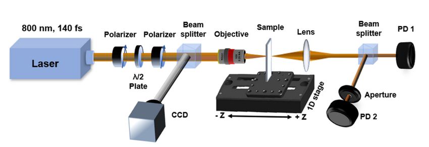
Abstract
We report a large third-order nonlinear optical response of palladium diselenide (PdSe2) lms – a two-
dimensional (2D) noble metal dichalcogenide material. Both open-aperture (OA) and closed-aperture (CA)
Z-scan measurements are performed with a femtosecond pulsed laser at 800 nm to investigate the
nonlinear absorption and nonlinear refraction, respectively. In the OA experiment, we observe optical
limiting behaviour originating from large two photo absorption (TPA) in the PdSe2 lm of β = 3.26 ×10− 8
m/W. In the CA experiment, we measure a peak-valley response corresponding to a large and negative
Kerr nonlinearity of n2 = -1.33×10− 15 m2/W – two orders of magnitude larger than bulk silicon. We also
characterize the variation of n2 as a function of laser intensity, observing that n2 decreases in magnitude
with incident laser intensity, becoming saturated at n2 = -9.96×10− 16 m2/W at high intensities. These
results verify the large third-order nonlinear optical response of 2D PdSe2 as well as its strong potential
for high performance nonlinear photonic devices.

Introduction
With their extraordinary nonlinear optical properties, two-dimensional (2D) layered materials such as
graphene [1-4], graphene oxide (GO) [5-9], transition metal dichalcogenides (TMDCs) [10-12], and black
phosphorus (BP) [13-15] have attracted a great deal of interest, enabling diverse nonlinear photonic
devices with vastly superior performance compared to bulk materials. Amongst them, TMDCs (MX2, M =
transition metal and X = chalcogen), with bandgaps in the near infrared to the visible region, have opened
up promising new avenues for photonic and optoelectronic devices. [2, 16]. Previously, the prominent
nonlinear optical properties of TMDCs such as MoS 2 [10, 17, 18], WS 2 [18-20] and MoSe2 [21, 22],
including a high Kerr nonlinearity and strong saturable absorption (SA), have been reported. These have
provided the basis of many nonlinear photonic devices for applications where, for example, a few mono-
layers of MoS 2 and WS 2 have been used as broadband, fast-recovery saturable absorbers for mode
locking in pulsed ber lasers [10, 23, 24]. In addition, nonlinear optical modulators and polarization
dependent all-optical switching devices have been realized based on ReSe2 [25] and SnSe [26].

Palladium diselenide (PdSe2), a new 2D noble metal dichalcogenide in the TMDC family, has recently
attracted signi cant interest [27-31]. Similar to the puckered structure of BP, it has a puckered pentagonal
atomic structure − with one Pd atom bonding to four Se atoms and two adjacent Se atoms covalently
bonding with each other. This low-symmetry structure makes PdSe2 possess unique in-plane anisotropic
optical and electronic properties [27, 29], featuring an in-plane noncentrosymmetric structure, in contrast
to its cousin PtSe2. Further, the bandgap of PdSe2 is layer-dependent, varying from 0 eV (bulk) to 1.3 eV
(monolayer) - a property well suited for photonic and optoelectronic applications – in particular, for
wavelength tuneable devices [27, 29, 31]. Moreover, PdSe2 is highly air-stable, indicating its robustness
and potential for practical applications as compared with BP. The high carrier mobility and anisotropic
Raman spectroscopy of 2D PdSe2 layers have been investigated [27, 30] as well as highly-sensitive

                                                  Page 2/18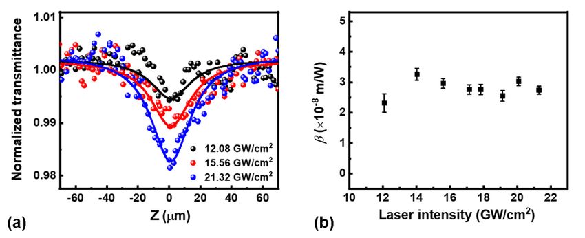
photodetectors from the visible to mid-infrared wavelengths [31, 32]. Recently, the optical nonlinear
absorption of PdSe2 nanosheets has also been reported in the context of mode-locked laser applications
[33-35]. To date, however, its optical Kerr nonlinearity has not been investigated.

Here, we report measurements of the third-order nonlinear optical response of 2D PdSe2 lms.
Experimental results using the Z-scan technique with femtosecond optical pulses at 800 nm show that
PdSe2 lms exhibit a large and negative (self-defocusing) Kerr nonlinearity (n2) of ∼ -1.33×10⁻¹⁵ m2/W,
which is two orders of magnitude larger than bulk silicon. Further, we measure a large nonlinear
absorption β of ~ 3.26 ×10⁻⁸ m/W, which originates from TPA in the PdSe2 lms. In addition, we
investigate the intensity dependence of the nonlinear response of PdSe2, nding that the absolute
magnitude of the Kerr nonlinearity n2 initially decreases slightly with incident laser intensity, becoming
saturated at higher intensities. Our results show that the extraordinary third-order nonlinear optical
properties of PdSe2 have strong potential for high-performance nonlinear photonic devices.

Material Preparation And Characterization
Figure 1(a) illustrates the atomic structure of PdSe2 crystals. The unique puckered pentagonal structure is
different to other TMDCs like MoS 2 and WS 2. The Se-Pd-Se layers stack with weak van der Waals
interactions to form a layered structure [27, 36, 37]. In each monolayer, the pentagonal rings are formed
with one Pd atom bonding to four Se atoms and two adjacent Se atoms covalently bonding with each
other, which is similar to the puckered structure of BP, and yields both anisotropic and non-
centrosymmetric properties of PdSe2 [27, 37]. More importantly, unlike the rapid degradation of BP under
ambient conditions, PdSe2 has signi cantly better air-stability [29-31]. Together, these properties of PdSe2
make it promising for high performance photonic and optoelectronic applications.

Here, we investigated large-area multilayer PdSe2 lms deposited on transparent sapphire substrates. The
PdSe2 lms were synthesized via Chemical vapor deposition (CVD) [30, 38]. A three-zone tube furnace
was used to grow the PdSe2 lms with palladium chloride (PdCl2) and selenium (Se) as precursors. Se
and PdCl2 powders were placed at Zone 1 with a heating temperature of 250 °C and Zone 2 heated up to
500 °C, respectively. The evaporated Se and Pd precursors were then transported by the carrier gas of
Ar/H2 to Zone 3 at a high temperature of 600 °C, in which the continuous PdSe2 lms were synthesized
on an atomically at sapphire substrate. The lms were polycrystalline, as is typical for CVD synthesized
 lms, with crystal sizes varying from 10’s of nanometres up to 100 nm. Because of the polycrystalline
nature of the lms, the inversion symmetry breaking properties (i.e., non-centrosymmetric) of the single
PdSe2 crystals could not be observed on optical wavelength scales in the macroscopic PdSe2 continuous
 lms studied in this work. Figure 1(b) shows a photograph of the prepared sample, indicating a high
uniformity over the whole substrate. The morphology image and height pro le of the prepared PdSe2
 lms were characterized by atomic force microscopy (AFM), as illustrated in Fig. 1(c). The lm thickness
was measured to be ~ 8 nm, which corresponds to ~20 layers of PdSe2 [27, 30, 36].

                                                  Page 3/18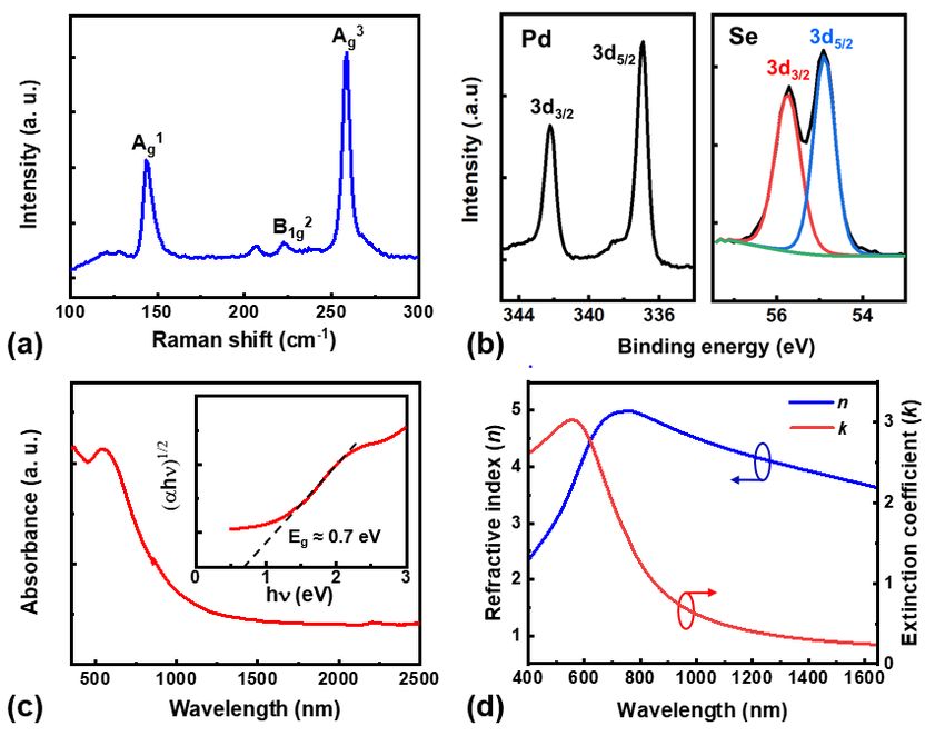
Figure 2(a) shows the Raman spectrum of the prepared PdSe2 lm excited with a laser at 514 nm. Three
representative phonon modes are observed, including the Ag1 (∼145.5 cm−1) and B1g2 (∼222.5 cm−1)
vibrational modes that correspond to the movement of Se atoms and the Ag3 (~ 258.8 cm−1) mode that
relates to the relative movements between Pd and Se atoms [27, 30, 32]. To further characterize the lm
quality, X-ray photoelectron spectroscopy (XPS) was employed to measure the binding energy of PdSe2.
Figure 2 (b) shows the XPS results of Pd 3d and Se 3d core levels for the PdSe2. The peaks of the t at ~
342.2 eV and ~ 336.9 eV are attributed to the Pd 3d3/2 and Pd 3d5/2, respectively, whereas the peaks at ~
55.7 eV and ~ 54.9 eV correspond to Se 3d3/2 and 3d5/2, respectively. These results are consistent with
previous reports [30, 32] and demonstrate the high quality of our prepared PdSe2 lms.

To characterize the linear absorption and optical bandgap, the optical absorption spectrum (from 400 nm
to 2500 nm) of the PdSe2 lm was measured with ultraviolet-visible (UV-vis) spectrometry, as shown in
Fig. 2(c). As expected, the linear absorption of the PdSe2 lm increased dramatically from the infrared to
visible wavelength regime. The optical bandgap of the PdSe2 lm can be estimated from a Tauc plot of
(αhν)1/2 versus hν based on the Tauc formula, where α and hν represent the optical absorption coe cient
and photon energy, respectively.[29, 32, 39] The inset of Fig. 2 (c) shows the Tauc plot extracted from the
linear absorption spectrum, where the optical bandgap of the PdSe2 lm is estimated to be ~ 0.7 eV and
shows good agreement with the reported values for 20 layers of PdSe2 in Refs. [29, 32].

We also characterize the in-plane (TE-polarized) refractive index (n) and extinction coe cient (k) of the
PdSe2 lm via spectral ellipsometry, as depicted in Fig. 2(d). For the thin PdSe2 lm with a thickness of
~8 nm, the out-of-plane (TM-polarized) response is much weaker. Thus, using spectral ellipsometry we
could only measure the in-plane n and k of the PdSe2 lm. It can be seen that the refractive index rst
increases dramatically with wavelength to reach a peak at ~ 700 nm and then decreases more gradually
at longer wavelengths. This trend is similar to that of PtSe2 – another noble metal dichalcogenide of the
TMDC family [40]. The extinction coe cient exhibits a signi cant decrease from 600 nm to 1200 nm, and
then the rate of decrease slows down at longer wavelengths. This shows an agreement with the trend of
the UV-vis absorption spectrum in Fig. 2 (c) and further con rms the validity of our ellipsometry
measurement. These measurements indicate that the lms had a bandgap of about 0.7 eV, residing just
below the telecommunications wavelength band.

Z-scan Measurement
3.1 Experimental setup

To investigate the third-order nonlinear optical properties of PdSe2, we characterized the nonlinear
absorption and refraction of the prepared PdSe2 lm via the Z-scan technique [14, 41, 42] (Fig. 3), where a
femtosecond pulsed laser with a centre wavelength at ~800 nm and pulse duration of ~ 140 fs was used
to excite the samples. A half-wave plate combined with a linear polarizer was employed to control the

                                                 Page 4/18
power of the incident light. A beam expansion system consisting of a 25-mm concave lens and 150-mm
convex lens was used to expand the light beam, which was then focused by an objective lens (10 ×, 0.25
NA) to achieve a low beam waist with a focal spot size of ~1.6 µm. The prepared samples were oriented
perpendicular to the beam axis and translated along the Z-axis with a linear motorized stage. A high-
de nition charge-coupled-device (CCD) imaging system was used to align the light beam to the target
sample. Two photodetectors (PDs) were employed to detect the transmitted light power for the signal and
reference arms.
The Z-scan measurements were performed in two stages [14, 41] including an open-aperture (OA) and
a closed aperture (CA) measurement. The OA measurement was used to characterize the nonlinear
absorption of PdSe2 lms where all light transmitted through the sample was collected by a PD. To
extract the TPA (β) of PdSe2, we t the measured OA results in Fig. 4(a) with [41, 43]: see formula 1 in the
supplementary les section.
where TOA(z) is the normalized optical transmittance; Leff = (1‒ e-α0L)/α0 is the effective sample
thickness; α0 is the linear absorption coe cient; L is the sample thickness; I0 is the irradiance intensity at
the focus; z is the sample position relative to the focus, and z0 is the Rayleigh length of the laser beam.
We also characterized the Kerr nonlinearity of the PdSe2 lm via the CA Z-scan experiment. In the CA
measurement, the change in the optical transmission results from both nonlinear absorption and the
nonlinear phase shift induced self-defocusing via the Kerr nonlinearity. The value of n2 for the PdSe2
lms at different laser intensities were extracted by tting the CA measurement with [41, 42] See formula
2 in the supplementary les section.
where TCA (z, ΔΦ0) is the normalized optical transmittance of the CA measurement and ΔΦ0 = 2πn2I0Leff/
λ is the nonlinear phase shift, with λ denoting the center wavelength of the femtosecond laser. Therefore,
the Kerr nonlinearity of the PdSe2 lm could be extracted from the ratio of the CA result to the OA result in
the usual manner [14, 41, 42].
3.2. Results and discussion
We measured the OA curves at different incident laser intensities ranging from 12.08 GW/cm2 to 21.32
GW/cm2. Figure 4(a) shows the OA Z-scan results for the PdSe2 lm at three representative intensities. A
typical optical limiting behaviour was observed in the OA curves, with the transmission decreasing as the
PdSe2 sample was moved through the focal point. We also note that the transmittance dip of the OA
curve decreased when the incident laser intensity was increased. Various mechanisms, including
nonlinear scattering, reverse saturable absorption (RSA) and two-photon absorption (TPA), may
contribute to the observed optical limiting behaviour. The nonlinear scattering mechanism is rst
excluded since it usually depends on the laser induced microbubble formation for dispersion or solution
samples [44, 45]. Usually, RSA is the dominant mechanism for nonlinear absorption under resonant or
near resonant excitation, while the TPA dominates under non-resonant excitation [46, 47]. In our case, the
Page 5/18incident laser of 800 nm is far from the resonant wavelength ( 1771 nm, corresponding to an optical
bandgap of 0.7 eV) of the PdSe2 lm. Therefore, the optical limiting behaviour is mainly attributed to
TPA. At low laser intensities, the linear absorption is dominant, while as the laser intensity increases,
increased photon population makes TPA possible, resulting in the excitation of electrons from the valence
to conduction bands.
To extract the TPA coe cient β of PdSe2, we t the measured OA results with Equation (1). The TPA
coe cient β for the PdSe2 lm is shown in Fig. 4(b) at different laser intensities. A large β = 3.26 ×10⁻⁸
m/W is observed, which is comparable to the reported values of graphene, and higher than that of WS 2,
highlighting the strong optical limiting effect in PdSe2 lm. In addition, the TPA coe cient β is relatively
constant with incident laser intensity, re ecting the fact that we are working in an intensity regime where
the material properties of the PdSe2 lms are not changing much. The slight uctuation in β with laser
intensity may arise from light scattering in the PdSe2 lm surface.
To further investigate the nonlinear absorption of the PdSe2 lm, we measured the minimum
transmittance with the sample at the focal point of the Z scan setup, for different incident laser
intensities. Figure 5(a) shows the transmittance of PdSe2 at the focal point as a function of laser
intensity, where the transmittance uctuates around a relatively constant value at low intensities and then
decreases signi cantly as the laser intensity increased. The experimental data ts the theory well [45],
verifying our assumption of TPA being the dominant process for nonlinear absorption in the PdSe2 lm.
The order of the observed nonlinear absorption can also be con rmed by examining the relation between
ln(1‒TOA) versus ln(I0) [48]: see formula 3 in the supplementary les.
where k is the slope showing the order of the nonlinear absorption and C is a constant. For pure TPA, the
slope is equal to 1 [48, 49]. We obtain a slope of 1.18 (Fig. 5(b)), suggesting the observed nonlinear
absorption is mainly attributed to TPA in the PdSe2 lm.
We also performed CA Z-scan measurements to investigate the Kerr nonlinearity (n2) of the PdSe2 lms.
The values of n2 for the PdSe2 lm at different laser intensities were extracted by tting the measured CA
results with Equation 2 [41, 42]. Figure 6(a) shows a representative CA result for PdSe2 at a laser intensity
of 21.32 GW/cm2. The transmittance of the sample exhibited a transition from peak to valley when the
sample passed through the focal plane. Such a peak-valley CA behaviour corresponds to a negative Kerr
coe cient n2 and indicates an optical self-defocusing effect in the PdSe2 lm. As discussed above, TPA
results in the transfer of electrons from valence band to conduction band, increasing the free carrier
density in the lm. Therefore, the observed negative Kerr nonlinearity potentially originates from the TPA-
induced free carrier nonlinear refraction and interband blocking [50-52].
Fig. 6(b) shows the measured Kerr coe cient n2 of PdSe2 versus laser intensity, showing a large n2 of
∼ ‒1.33×10⁻¹⁵ m2/W. Table 1 compares the β and n2 of PdSe2 with other 2D layered materials. As can be
seen, the value of n2 for PdSe2 is lower than those of graphene and GO, but still more than two orders of
Page 6/18magnitude higher than bulk silicon [53, 54]. Such a high n2 suggests that PdSe2 is an extremely
promising material for self-defocusing based nonlinear photonic applications. For example, a negative
Kerr nonlinearity can be used to self-compress ultrashort pulses in the presence of positive group-velocity
dispersion [55, 56]. Another application of a negative Kerr nonlinearity is mode locking of lasers using the
Kerr mode-locking technique [53, 57] as well as the possibility of achieving net parametric modulational
instability gain under normal dispersion conditions [53, 58].
Moreover, as shown in Fig. 6(b), the absolute value of n2 initially decreases with laser intensity and then
saturates at higher intensities. In theory, the optical nonlinear refraction originates mainly from the free-
carrier and bound-electron nonlinearities [51, 59, 60]. We assume that both mechanisms exist in PdSe2
lms. The refractive index change in the PdSe2 lm can be expressed by Δn = n2*I0 + σrN, where n2* is the
nonlinear refraction related to bonding electrons, σr is the free carrier refractive coe cient and N is the
charge carrier density.[51] Therefore, the effective n2 = Δn/I0 = n2* + σrN/I0, is an intensity dependent
parameter, which can explain the n2 variation as a function of laser intensity observed in our
measurements.
Table 1. Comparison of β and n2for various 2D layered materials
Material Laser Thickness β (m/W) n2(m2/W) n2(×n2 of Ref.
parameter
Si1)
Graphene 1150 nm, 5-7 layers 3.8 × 10⁻⁸ -5.5 × 10⁻¹⁴ -1.22 × [61]
100 fs 104
GO 800 nm, 100 ∼2 µm 4 × 10⁻⁷ 1.25 × 10⁻¹³ 2.75 × [62]
fs 104
MoS 2 1064 nm, 25 ∼25 µm (-3.8 ± 0.59) × (1.88 ± 0.48) × 41.32 [18]
ps 10−11 10-16
WS 2 1040 nm, ∼57.9 nm (1.81 ± 0.08) × (-3.36 ± 0.27) × -73.85 [19]
340 fs 10−8 10-16
BP 1030 nm, ∼15 nm 5.845 × 10⁻⁶ -1.635 × 10⁻¹² -3.59 × [14]
140 fs 105
PtSe2 800 nm, 150 ∼4.6 nm -8.80 × 10⁻⁸ − − [63]
fs
PtSe2 1030 nm, 17 layers − (-3.76 ± 0.46) × -8.26 × [48]
340 fs 10-15 102
PdSe2 800 nm, 140 ∼8 nm (3.26 ± 0.19) × (-1.33 ± 0.23) × -2.92 × This
fs 10−8 10-15 102 work
1
n2 for silicon = 4.55 × 10⁻¹⁸ m2/W (ref. [54] )
Page 7/18In contrasting the Kerr 3rd order nonlinearity and TPA with other 3rd order effects such as optical third
harmonic generation (THG) [64-69] it is interesting to note that unlike THG, both the sign and phase of the
Kerr nonlinearity are critically important. The concept of the nonlinear FOM was originally proposed
purely in the context of a limitation for n2 devices having a positive n2 and TPA. Here, the fact that n2 for
PdSe2 is negative means that the conventional importance of a large FOM is probably not applicable.
Further, TPA has been known to potentially have a positive impact on some signal processing functions
[70-72] and so the large TPA of PdSe2 is a potential advantage to this material. The combination of a
large and negative n2 with a very large TPA makes PdSe2a highly interesting material for novel nonlinear
processes that can exploit self-defocusing effects. It is signi cantly different to graphene oxide [73-83] in
terms of both the Kerr nonlinearity and nonlinear absorption. It may offer interesting advantages when
combined with advanced SOI photonic circuits [84-87] to yield advanced nonlinear functions.
Conclusion
We report a large third-order nonlinear optical response of PdSe2 lms measured with the Z-scan
technique. Our results show that PdSe2 has a strong TPA response with a large β of ~ 3.26 ×10⁻⁸ m/W.
We also investigate the Kerr nonlinearity (n2) of PdSe2 nding that n2 is negative, and with an absolute
magnitude that is more than two orders of magnitude larger than bulk silicon. Furthermore, the variation
in n2 of PdSe2 with laser intensity is characterized. We nd that n2 initially increases (decreasing in
absolute magnitude) with incident laser intensity and then saturates at higher intensities. These results
verify PdSe2 as a promising 2D material with prominent nonlinear optical properties.
Declarations
Competing interests: The authors declare no competing interests.
Acknowledgements
This work was supported by the Australian Research Council Discovery Projects Program (No.
DP150102972 and DP190103186), and the Industrial Transformation Training Centres scheme (Grant
No. IC180100005). We acknowledge Swinburne Nano Lab and Micro Nano Research Facility (MNRF) of
RMIT University for the support in material characterization as well as Shenzhen Sixcarbon Technology
for the PdSe2 lm fabrication. We thank Dr. Yunyi Yang and Dr. Tania Moein for technical support, Dr.
Deming Zhu for assisting in XPS characterization and Dr. Chenglong Xu for assisting in optical
characterization.
References
[1] G.-K. Lim et al., "Giant broadband nonlinear optical absorption response in dispersed graphene
single sheets," Nature Photonics, vol. 5, no. 9, pp. 554-560, 2011.
Page 8/18[2] A. Autere et al., "Nonlinear Optics with 2D Layered Materials," Advanced Materials, vol. 30, no. 24,
p. e 1705963, 2018.
[3] Y. Yang et al., "High-e ciency and broadband four-wave mixing in a silicon-graphene strip
waveguide with a windowed silica top layer," Photonics Research, vol. 6, no. 10, pp. 100965-70, 2018.
[4] T. Pan et al., "Analysis of an electro-optic modulator based on a graphene-silicon hybrid 1D
photonic crystal nanobeam cavity," Opt Express, vol. 23, no. 18, pp. 23357-64, 2015.
[5] Y. Yang et al., "Invited Article: Enhanced four-wave mixing in waveguides integrated with
graphene oxide," APL Photonics, vol. 3, no. 12, p. e 120803, 2018; doi: 10.1063/1.5045509.
[6] Y. Yang et al., "Graphene-based multilayered metamaterials with phototunable architecture for
on-chip photonic devices," ACS Photonics, vol. 6, no. 4, pp. 1033-1040, 2019.
[7] J. Wu et al., "Graphene oxide waveguide and micro‐ring resonator polarizers," Laser & Photonics
Reviews, vol. 13, no. 9, p. e 1900056, 2019.
[8] J. Wu et al., "2D Layered graphene oxide lms integrated with micro-ring resonators for enhanced
nonlinear optics," Small, vol. 16, no. 16, p. e 1906563, 2020.
[9] Y. Zhang et al., "Enhanced nonlinear optical gure-of-merit at 1550nm for silicon nanowires
integrated with graphene oxide layered lms," arXiv:2004.08043, 2020.
[10] S. Wang et al., "Broadband few-layer MoS 2 saturable absorbers," Advanced Materials, vol. 26, no.
21, pp. 3538 - 3544, 2014.
[11] H. Chen et al., "Enhanced second-harmonic generation from two-dimensional MoSe2 on a silicon
waveguide," Light: Science & Applications, vol. 6, no. 10, p. e 17060, 2017.
[12] H. Liu et al., "High-harmonic generation from an atomically thin semiconductor," Nature Physics,
vol. 13, no. 3, pp. 262-265, 2016.
[13] X. Zheng et al., "Characterization of nonlinear properties of black phosphorus nanoplatelets with
femtosecond pulsed Z-scan measurements," Optics Letters, vol. 40, no. 15, pp. 3480-3, 2015.
[14] T. Yang et al., "Anisotropic third-order nonlinearity in pristine and lithium hydride intercalated
black phosphorus," ACS Photonics, vol. 5, no. 12, pp. 4969-4977, 2018.
[15] Z. C. Luo et al., "Micro ber-based few-layer black phosphorus saturable absorber for ultra-fast
ber laser," Optics Express, vol. 23, no. 15, pp. 20030-9, 2015.
[16] X. Liu et al., "Emerging low-dimensional materials for nonlinear optics and ultrafast photonics,"
Advanced Materials, vol. 29, no. 14, p. e 1605886, 2017.
Page 9/18[17] S. Zhang et al., "Direct observation of degenerate two-photon absorption and its saturation in
WS 2 and MoS 2 monolayer and few-layer lms," ACS Nano, vol. 9, no. 7, pp. 7142-7150, 2015.
[18] S. Bikorimana et al., "Nonlinear optical response in two-dimensional transition metal
dichalcogenide multilayer: WS 2, WSe2, MoS 2 and Mo0.5W0.5S 2," Optics Express, vol. 24, no. 18, pp. 20685-
95, 2016.
[19] N. Dong et al., "Dispersion of nonlinear refractive index in layered WS 2 and WSe2 semiconductor
lms induced by two-photon absorption," Optics Letters, vol. 41, no. 17, pp. 3936-3939, 2016.
[20] X. Zheng et al., "Z-scan measurement of the nonlinear refractive index of monolayer WS 2," Optics
Express, vol. 23, no. 12, pp. 15616-23, 2015.
[21] K. Wang et al., "Broadband ultrafast nonlinear absorption and nonlinear refraction of layered
molybdenum dichalcogenide semiconductors," Nanoscale, vol. 6, no. 18, pp. 10530-5, 2014.
[22] N. Dong et al., "Saturation of Two-Photon Absorption in Layered Transition Metal
Dichalcogenides: Experiment and Theory," ACS Photonics, vol. 5, no. 4, pp. 1558-1565, 2018.
[23] B. Chen et al., "Q-switched ber laser based on transition metal dichalcogenides MoS 2, MoSe2,
WS 2, and WSe2," Optics Express, vol. 23, no. 20, pp. 26723-37, 2015.
[24] K. Wu et al., "WS 2 as a saturable absorber for ultrafast photonic applications of mode-locked
and Q-switched lasers," Optics Express, vol. 23, no. 9, pp. 11453-61, 2015.
[25] L. Du et al., "Few-layer rhenium diselenide: an ambient-stable nonlinear optical modulator,"
Optical Materials Express, vol. 8, no. 4, pp. 926-935, 2018.
[26] C. Zhang et al., "Anisotropic nonlinear optical properties of a SnSe ake and a novel perspective
for the application of all‐optical switching," Advanced Optical Materials, vol. 7, no. 18, p. e 1900631, 2019.
[27] A. D. Oyedele et al., "PdSe2: Pentagonal two-dimensional layers with high air stability for
electronics," J Am Chem Soc, vol. 139, no. 40, pp. 14090-14097, 2017.
[28] G. D. Nguyen et al., "3D Imaging and manipulation of subsurface selenium vacancies in PdSe2,"
Physical Review Letters, vol. 121, no. 8, p. e 086101, 2018.
[29] G. Zhang et al., "Optical and electrical properties of two-dimensional palladium diselenide,"
Applied Physics Letters, vol. 114, no. 25, p. e 253102, 2019.
[30] S. Jiang et al., "Anisotropic growth and scanning tunneling microscopy identi cation of ultrathin
even-layered PdSe2 ribbons," Small, vol. 15, no. 45, p. e 1902789, 2019.
Page 10/18[31] Q. Liang et al., "High-Performance, room temperature, ultra-broadband photodetectors based on
air-stable PdSe2," Advanced Materials, vol. 31, no. 24, p. e1807609, 2019.
[32] L.-H. Zeng et al., "Controlled synthesis of 2D PdSe2 for sensitive photodetector applications,"
Advanced Functional Materials, vol. 29, no. 1, p. e1806878, 2019.
[33] Ziqi Li et al., "Generation of multi-gigahertz laser pulses in optical lattice-like cladding
waveguides with PdSe2 as a new saturable absorber," 2019 CLEO Europe and EQEC, 1, 2019.
[34] Y. Ma et al., "Passively Q-switched Nd:GdLaNbO4 laser based on 2D PdSe2 nanosheet," Optics &
Laser Technology, vol. 124, p. e105959, 2019.
[35] H. Zhang et al., "Palladium selenide as a broadband saturable absorber for ultra-fast photonics,"
Nanophotonics, https://doi.org/10.1515/nanoph-2020-0116, 2020.
[36] J. Sun et al., "Electronic, transport, and optical properties of bulk and mono-layer PdSe2," Applied
Physics Letters, vol. 107, no. 15, p. e153902, 2015.
[37] C. Long et al., "PdSe2: exible two-dimensional transition metal dichalcogenides monolayer for
water splitting photocatalyst with extremely low recombination rate," ACS Applied Energy Materials, vol. 2,
no. 1, pp. 513-520, 2018.
[38] H. Xu et al., "Controlled doping of wafer-scale PtSe2 lms for device application," Advanced
Functional Materials, vol. 29, no. 4, p. e 1805614, 2019.
[39] H. Feng et al., "Modulation of photocatalytic properties by strain in 2D BiOBr nanosheets," ACS
Appl Mater Interfaces, vol. 7, no. 50, pp. 27592-6, 2015.
[40] J. Xie et al., "Optical properties of chemical vapor deposition-grown PtSe2 characterized by
spectroscopic ellipsometry," 2D Materials, vol. 6, no. 3, p. e 035011, 2019.
[41] L. Jia et al., "Highly nonlinear BiOBr nano akes for hybrid integrated photonics," APL Photonics,
vol. 4, no. 9, p. e 090802, 2019.
[42] M. Sheik-Bahae et al.,"Sensitive measurement of optical nonlinearities using a single beam," IEEE
JOURNAL OF QUANTUM ELECTRONICS, vol. 26, no. 4, pp. 760-769, 1990.
[43] P. Li et al., "Two-dimensional CH3NH3PbI3 perovskite nanosheets for ultrafast pulsed ber lasers,"
ACS Appl Mater Interfaces, vol. 9, no. 14, pp. 12759-12765, 2017.
[44] P. Chantharasupawong et al., "Optical power limiting in uorinated graphene oxide: an insight
into the nonlinear optical properties," The Journal of Physical Chemistry C, vol. 116, no. 49, pp. 25955-61,
2012.
Page 11/18[45] G. Wang et al., "Two‐photon absorption in monolayer Mxenes," Advanced Optical Materials,
https://doi.org/10.1002/adom.201902021, p. e 1902021, 2020.
[46] Z. Liu et al., "Nonlinear optical properties of graphene oxide in nanosecond and picosecond
regimes," Applied Physics Letters, vol. 94, no. 2, p.e 021902, 2009.
[47] P. P. Kiran et al.,"Contribution of two-photon and excited state absorption in ‘axial-bonding’ type
hybrid porphyrin arrays under resonant electronic excitation," Chemical Physics Letters, vol. 418, no. 4-6,
pp. 442-447, 2006.
[48] L. Wang et al., "Nonlinear optical signatures of the transition from semiconductor to semimetal
in PtSe2," Laser & Photonics Reviews, vol. 13, no. 8, p. e 1900052, 2019.
[49] Y. Q. et al., "Three-photon absorption in ZnO and ZnS crystals," Optics Express, vol. 13, no. 23, pp.
9235-9247, 2005.
[50] D. J. Hagan et al., "Self-protecting semiconductor optical limiters," Optics Letters, vol. 13, no. 4,
pp. 315-317, 1988.
[51] A. A. Said et al., "Determination of bound-electronic and free-carrier nonlinearities in ZnSe, GaAs,
CdTe, and ZnTe," J. Opt. Soc. Am. B, vol. 9, no. 3, pp. 405-414, 1992.
[52] R. W. Boyd, "Nonlinear Optics," Elsevier: Singapore, 2003.
[53] A.Pasquazi, et al., “Micro-Combs: A Novel Generation of Optical Sources”, Physics Reports vol.
729, 1–81, 2018.
[54] D. J. Moss et al., "New CMOS-compatible platforms based on silicon nitride and Hydex for
nonlinear optics," Nature Photonics, vol. 7, no. 8, pp. 597-607, 2013.
[55] R. DeSalvo et al., "Self-focusing and self-defocusing by cascaded second-order effects in KTP,"
Optics Letters, vol. 17, no. 1, pp. 28-30, 1992.
[56] M. Seidel et al., "E cient high-power ultrashort pulse compression in self-defocusing bulk
media," Scienti c Reports, vol. 7, no. 1, p. e 1410, 2017.
[57] C. Kriso et al., "Microcavity-enhanced Kerr nonlinearity in a vertical-external-cavity surface-
emitting laser," Optics Express, vol. 27, no. 9, pp. 11914-29, 2019.
[58] Y. Liu et al., "Investigation of mode coupling in normal-dispersion silicon nitride microresonators
for Kerr frequency comb generation," Optica, vol. 1, no. 3, pp. 137-144, 2014.
[59] S. Lu et al., "Third order nonlinear optical property of Bi2Se3," Optics Express, vol. 21, no. 2, pp.
2072-2082, 2013.
Page 12/18[60] M. Sheik-Bahae et al., "Dispersion of bound electronic nonlinear refraction in solids," IEEE
JOURNAL OF QUANTUM ELECTRONICS, vol. 27, no. 6, pp. 1296-1309, 1991.
[61] G. Demetriou et al., "Nonlinear optical properties of multilayer graphene in the infrared," Optics
Express, vol. 24, no. 12, pp. 13033-43, 2016.
[62] X. Zheng et al., "In situ third-order non-linear responses during laser reduction of graphene oxide
thin lms towards on-chip non-linear photonic devices," Advanced Materials, vol. 26, no. 17, pp. 2699-
2703, 2014.
[63] G. Wang et al., "Ultrafast carrier dynamics and bandgap renormalization in layered PtSe2," Small,
vol. 15, no. 34, p. e1902728, 2019.
[64] D. J. Moss, H. M. van Driel, and J. E. Sipe, Opt. Lett. 14 (1), 57 (1989).
[65] J. E. Sipe, D. J. Moss, and H. M. van Driel, Phys. Rev. B 35 (3), 1129 (1987).
[66] D. J. Moss, E. Ghahramani, J. E. Sipe, and H. M. van Driel, Phys. Rev. B 41 (3), 1542 (1990).
[67] D. J. Moss, H. M. van Driel, and J. E. Sipe, Appl. Phy. Lett. 48 (17) 1150 (1986).
[68] Monat, C. et al., Optics Express 18 (7), 6831-6840 (2010). DOI: 10.1364/OE.18.006831.
[69] C.Monat et al., Nature Communications 5 Article:3246 (2014). doi:10.1038/ncomms4246.
[70] D.J.Moss, et al., Electronics Letters 41 320 (2005). DOI:10.1049/el:20058051
[71] M.R.E. Lamont, et al., Photonics Technology Letters 18 1185 (2006).
DOI:10.1109/LPT.2006.874718.
[72] A.Tuniz, G.Brawley, D.J.Moss, B.J.Eggleton,, Optics Express 16 18524 (2008).
DOI: 10.1364/OE.16.018524.
[73] Yang Qu, Jiayang Wu, Yuning Zhang, Yao Liang, Baohua Jia, and David J. Moss, “Analysis of four-
wave mixing in silicon nitride waveguides integrated with 2D layered graphene oxide lms”, Journal of
Lightwave Technology, vol. 39, Early Access (2021). DOI: 10.1109/JLT.2021.3059721.
[74] Yuning Zhang, Jiayang Wu, Yang Qu, Linnan Jia, Baohua Jia, and David J. Moss, “Analysis of self-
phase modulation in silicon-on-insulator nanowires integrated with 2D layered graphene oxide lms,
Journal of Lightwave Technology, Early Access (2021). DOI: 10.1109/JLT.2021.3069733
[75] Moss, David. “Design of silicon waveguides integrated with 2D graphene oxide lms for Kerr
nonlinear optics”. TechRxiv. Preprint. (2020), DOI:36227/techrxiv.13203278.v1
Page 13/18[76] Zhang, Y.; Wu, J.; Qu, Y.; Jia, L.; Jia, B.; Moss, D., “Design of Silicon Waveguides Integrated with 2D
Graphene Oxide Films for Kerr Nonlinear Optics”, Preprints (2020), 2020110279.
[77] Wu, J., Jia, L., Zhang, N., Qu, Y., Jia, B. and Moss, D. J., “Graphene Oxide for Integrated Photonics and
Flat Optics”, Advanced Materials, Vol 32, 1-29, 2006415 (2020). DOI:10.1002/adma.202006415.
[78] Yang, Y.; Wu, J.; Xu, X.; Liang, Y.; Chu, S. T.; Little, B. E.; Morandotti, R.; Jia, B.; Moss, D. J., “Invited
Article: Enhanced four-wave mixing in waveguides integrated with graphene oxide”, APL Photonics, vol. 3,
120803 (2018).
[79] Zhang, Y.; Wu, J.; Yang, Y.; Qu, Y.; Jia, L.; Moein, T.; Jia, B.; Moss, D. J., “Enhanced Kerr Nonlinearity and
Nonlinear Figure of Merit in Silicon Nanowires Integrated with 2D Graphene Oxide Films”, ACS Applied
Materials and Interfaces, vol.12, pp.33094-33103 (2020). DOI:10.1021/acsami.0c07852.
[80] Qu, Y., Wu, J., Yang, Y., Zhang, N., Liang, Y., Dirani, H. E., Crochemore, R., Demongodin, P.,
Sciancalepore, C., Grillet, C., Monat, C., Jia, B., David J. Moss, “Enhanced Four‐Wave Mixing in Silicon
Nitride Waveguides Integrated with 2D Layered Graphene Oxide Films”, Advanced Optical Materials, Vol.
8, 2001048 (2020). DOI: 10.1002/adom.202001048.
[81] Yuning Zhang, Jiayang Wu, Yang Qu, Linnan Jia, Baohua Jia, and David J. Moss, "Design of silicon
waveguides integrated with 2D graphene oxide lms for Kerr nonlinear optics", Journal of Lightwave
Technology, Vol. 39, Early Access (2021). DOI: 10.1109/JLT.2021.3069733.
[82] Jia, J. Wu, T. Yang, B. Jia, D. J. Moss, “Large Third-Order Optical Nonlinearity in 2D PdSe2
Dichalcogenide Films for Nonlinear Photonic Devices”, Paper No. 11689-34, PW21O-OE201-68, Integrated
Optics: Devices, Materials, and Technologies XXV, SPIE Photonics West, San Francisco CA March 6-11
(2021). doi.org/10.1117/12.2584029
[83] Qu, J. Wu, Y. Zhang, L. Jia, Y. Yang, X. Xu, S. T. Chu, B. E. Little, R. Morandotti, B. Jia, and D. J. Moss,
“Graphene oxide for enhanced optical nonlinear performance in CMOS compatible integrated devices”,
Paper No. 11688-30, PW21O-OE109-36, 2D Photonic Materials and Devices IV, SPIE Photonics West, San
Francisco CA March 6-11 (2021). doi.org/10.1117/12.2583978
[84] Wu, T. Moein, X. Xu et al., "Micro-ring resonator quality factor enhancement via an integrated Fabry-
Perot cavity," APL Photonics, Vol.2, No. 5, 056103 (2017). doi: 10.1063/1.4981392.
[85] Wu, T. Moein, X. Xu et al., "Advanced photonic lters based on cascaded Sagnac loop re ector
resonators in silicon-on-insulator nanowires," APL Photonics, Vol. 3, No. 4, 046102 (2018).
DOI:/10.1063/1.5025833.
[86] Arianfard, J. Wu, S. Juodkazis et al., "Advanced multi-functional integrated photonic lters based on
coupled Sagnac loop re ectors," Journal of Lightwave Technology, Vol. 39, Issue: 5, pp.1400-1408 (2021).
DOI:10.1109/JLT.2020.3037559.
Page 14/18[87] Arianfard, J. Wu, S. Juodkazis, and D.J.Moss, "Three coupled waveguide Sagnac loop re ectors for
high performance integrated optical lters," Journal of Lightwave Technology, Vol. 39, Early Access
(2021). DOI: 10.1109/JLT.2021.3066256.
Figures
Figure 1
(a) Crystal structure of PdSe2. (b) Photograph of prepared multilayer PdSe2 lm. The unit for the
numbers on the ruler is centimeter. (c) AFM height pro le of the multilayer PdSe2 lm.
Page 15/18Figure 2
Characterization of the prepared PdSe2 lm. (a) Raman spectrum excited via a 514-nm laser. (b) X-ray
photoelectron spectroscopy (XPS) spectra. (c) UV-vis absorption spectrum. Inset shows the extracted
Tauc plot. (d) Measured refractive index (n) and extinction coe cient (k).
Page 16/18Figure 3
Schematic illustration of Z-scan experimental setup. PD: power detector.
Figure 4
(a) OA Z-scan results of PdSe2 lm at different intensities. (b) TPA coe cient β of PdSe2 lm versus
laser intensity.
Page 17/18Figure 5
(a) Normalized transmittance of PdSe2 lm at the focal point as a function of laser intensity. (b) The plot
of ln(1−TOA) versus ln(I0) to determine the order of nonlinearity. The measured and t results are shown
by scatter data points and solid lines, respectively.
Figure 6
(a) CA Z-scan result of PdSe2 lm at intensity of 21.32 GW/cm2. (b) Kerr coe cient n2 of PdSe2 lm
versus laser intensity.
Supplementary Files
This is a list of supplementary les associated with this preprint. Click to download.
formula.docx
Page 18/18You can also read