Meta-optics for spatial optical analog computing - De Gruyter
←
→
Page content transcription
If your browser does not render page correctly, please read the page content below
Nanophotonics 2020; 9(13): 4075–4095

Review

Sajjad Abdollahramezani, Omid Hemmatyar and Ali Adibi*

Meta-optics for spatial optical analog computing
https://doi.org/10.1515/nanoph-2020-0285                                         1 Introduction
Received May 13, 2020; accepted August 25, 2020; published online
September 7, 2020
                                                                                 For decades, optics has proved to be an unrivaled means of
                                                                                 communication between two points as close as two chip-
Abstract: Rapidly growing demands for high-performance
                                                                                 scale modules or as far as two intercontinental data cen-
computing, powerful data processing, and big data necessi-
                                                                                 ters. To a similar extent, optical computing has been
tate theadvent ofnoveloptical devicesto perform demanding
                                                                                 overshadowed by powerful digital computers empowered
computing processes effectively. Due to its unprecedented
                                                                                 by highly integrable transistors as mature electronic
growth in the past two decades, the field of meta-optics offers
                                                                                 switches. However, when it comes to intricate problems
a viable solution for spatially, spectrally, and/or even
                                                                                 such as optimization dealing with very large data sets,
temporally sculpting amplitude, phase, polarization, and/or
                                                                                 even breakthrough application-specific integrated circuit
dispersion of optical wavefronts. In this review, we discuss
                                                                                 technologies such as a tensor processing unit have
state-of-the-art developments, as well as emerging trends, in
                                                                                 shown substantial limitations in practice [1]. All-optical
computational metastructures as disruptive platforms for
                                                                                 computing holds the promise to solve challenging prob-
spatial optical analog computation. Two fundamental ap-
                                                                                 lems such as large-scale combinatorial optimizations [2, 3]
proaches based on general concepts of spatial Fourier trans-
                                                                                 and probabilistic graphical models [4], which have found
formation and Green’s function (GF) are discussed in detail.
                                                                                 many practical applications in artificial intelligence, image
Moreover, numerical investigations and experimental dem-
                                                                                 processing, and social networks.
onstrations of computational optical surfaces and meta-
                                                                                      Optical computing generally refers to the numerical
structures for solving a diverse set of mathematical problems
                                                                                 computation of one-dimensional or multidimensional data
(e.g., integrodifferentiation and convolution equations)
                                                                                 using photons as the primary carrier medium. Optical
necessary for on-demand information processing (e.g., edge
                                                                                 computing has been an active field of research for over 60
detection) are reviewed. Finally, we explore the current
                                                                                 years with impressive achievements in analog/digital and
challenges and the potential resolutions in computational
                                                                                 classic/quantum information processing that leverage
meta-optics followed by our perspective on future research
                                                                                 various computational approaches including Turing ma-
directions and possible developments in this promising area.
                                                                                 chines, brain-inspired neuromorphic architectures, and
Keywords: edge sensing; Fourier transformation; Green’s                          metaphoric systems. Optical computing as a serious rival
function; metasurfaces; optical analog computing.                                has experienced ups and downs in different time periods [5–
                                                                                 7]. This stems from the indisputable superiority of optical
                                                                                 technology in some important aspects including inherent
                                                                                 parallel processing, low cross talk, passive components
                                                                                 with zero static energy consumption, and high space and
                                                                                 time bandwidth products that potentially alleviate the
                                                                                 inherent shortcomings of digital electronics, namely speed,
                                                                                 heat generation, and power hungriness [7–9]. Although
Sajjad Abdollahramezani and Omid Hemmatyar contributed equally                   early attempts have been devoted to digital optical
to this article.
                                                                                 computing by mimicking the principles of electronic com-
*Corresponding author: Ali Adibi, School of Electrical and Computer              puters, people found the eventual goal out of reach due to
Engineering, Georgia Institute of Technology, 778 Atlantic Drive NW,             the lack of small-footprint and energy-efficient nonlinear
Atlanta, GA 30332-0250, USA, E-mail: ali.adibi@ece.gatech.edu                    elements working as functional optical switches [10]. In this
Sajjad Abdollahramezani and Omid Hemmatyar, School of Electrical                 regard, optical analog computing has gained more attrac-
and Computer Engineering, Georgia Institute of Technology, 778
                                                                                 tion leading to more striking developments in recent years.
Atlantic Drive NW, Atlanta, GA 30332-0250, USA,
E-mail: ramezani@gatech.edu (S. Abdollahramezani),                               Generally, analog optical computing can be classified into
omid.hemmatyar@gatech.edu (O. Hemmatyar)                                         (i) linear platforms enabling space-invariant operations

  Open Access. © 2020 Sajjad Abdollahramezani et al., published by De Gruyter.             This work is licensed under the Creative Commons Attribution
4.0 International License.
4076           S. Abdollahramezani et al.: Meta-optics for spatial optical analog computing

(such as correlation and convolution), as well as space-                 miniaturized configurations. As the most interesting
variant operations (such as Hough or coordinates trans-                  paradigm, metastructures (including both metamaterials
form), and (ii) nonlinear systems enabling pivotal opera-                and metasurfaces [12–33]) hold great promise to imprint
tions such as logarithm transformation, as well as                       the desired transformations in amplitude, phase, and
thresholding [5, 11]. Due to the vast diversity of achieve-              polarization of the impinging light thanks to the (sub)
ments in each field, we limit the scope of this review to the             wavelength-scale scatterers with optimized size, shape,
spatial optical analog computing within the linear shift-                orientation, and composition.
invariant (LSI) systems.                                                     Motivated by such technological developments,
     Over the past six decades, spatial analog optical                   Engheta et al. recently introduced the concept of
computing has been arguably indebted to the progress in                  “computational metamaterials” [34]. These structures
game-changing technologies such as diffractive and                       perform mathematical operations by direct manipulation
refractive optical elements, holograms, spatial light                    of propagating light waves through judiciously designed
modulators (SLMs), and microelectromechanical mirrors                    metamaterial and metasurface platforms. This work
[11]. However, computing systems established based on                    inspired an ever-increasing interest to propose and
those components are complex, challenging to align, and                  demonstrate viable solutions to expand the horizon of
bulky in size, hindering integration with compact nano-                  small-footprint computational systems for on-demand
photonic circuits. Recent extraordinary advances in                      applications ranging from complex mathematical opera-
nanofabrication have pushed the thickness limit of                       tions to real-time edge detection and large-scale image
various optical elements deep into the nanometric scale,                 processing to machine vision. Two fundamental ap-
enabling stronger interaction of light–matter necessary                  proaches have been pursued so far to realize computa-
for full control over the properties of incident light in                tional meta-optics: (i) spatial Fourier transfer approach,

 A                           Spatial Fourier Transfer Approach                B                          Green’s Function Approach

Metalens
   ℱ

          Metasurface                                                                                  Metasurface
             H(kx)                                                                                      H(kx, ky)

                            Metalens
                               ℱ
   First-order spatial differentiator                                          Second-order spatial differentiator

Figure 1: Computational meta-optics. Conceptual representation of spatial analog computing based on general concepts of (A) spatial Fourier
transfer and (B) Green’s function (GF) approach. The former leverages a 4f correlator system formed by two series lenses with equal focal
lengths and an intermediate complex-valued spatial filter located at the shared focal plane. The first metalens transforms the incident light
with a spatially variant profile (Gaussian in this example) to the Fourier domain (i.e., k-space), while the second metalens transfers back the
light processed by the intermediate metasurface to the spatial domain. The transfer function (i.e., H(kx)) associated with the kernel of the
operator of choice, one-dimensional (1D) first-order differentiation in this example, is encoded into the metasurface. The latter takes
advantage of the nonlocal response of an engineered single-layer optical surface or a multilayered slab that performs the desired kernel of
choice. The computational system in (B) performs the second-order spatial derivation for two-dimensional (2D) edge detection.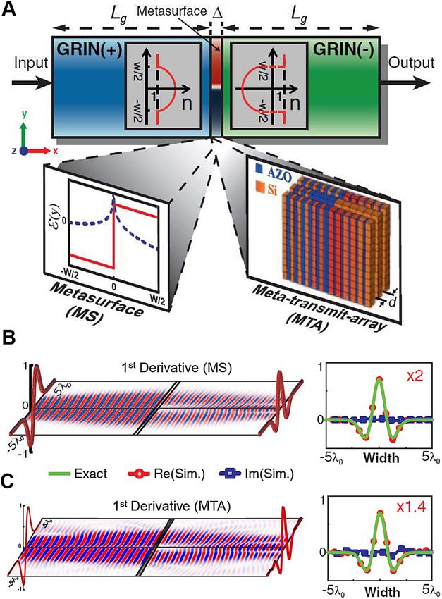
S. Abdollahramezani et al.: Meta-optics for spatial optical analog computing    4077

in which a 4f system incorporating a metascreen for                        powerful concept can be applied to a metaprocessor given
realization of the desired transfer function is employed,                  that f (x, y) and g (x, y) are the field profiles of the incident
and (ii) Green’s function (GF) approach, in which a                        and transmitted/reflected optical beams, respectively. In
resonant or nonresonant metascreen is utilized to realize                  this regard, the transfer function of the system, i.e., H (kx,
the desired spatial impulse response associated with the                   ky), associated with the desired mathematical operator of
mathematical operator of choice (see conceptual images                     choice can be implemented by employing a spatially
in Figure 1). In the following sections, we first elaborate                 variant subblock with position-dependent transmission/
basic principles of each approach and then discuss rele-                   reflection coefficient. It is noteworthy that the realization
vant recent developments. These new paradigms offer                        of an inverse Fourier transform subblock with natural
real-time spatial wave-based processing mechanisms                         materials is not practically feasible. Based on the well-
through miniaturized all-optical computing machines or                     known relation F {F {A(x, y)}} ∝ A(−x, −y), a Fourier lens
potentially integratable hardware accelerators.                            can be used instead to perform inverse Fourier transform
                                                                           operation at the expense of image mirroring of the desired
                                                                           output [34].
                                                                                Many scientific phenomena and engineering problems
2 Spatial Fourier transfer approach
                                                                           such as heat transfer, electromagnetic radiation, Kirchh-
This approach has been investigated for decades in 4f                      off’s second law in circuit analysis can be described
correlators using bulky optical components [11]. Inspired                  through a system of partial differential, integral, and
by conventional 4f systems, the generic architecture of an                 integrodifferential equations. As such, finding the exact
optical metaprocessor is formed by the integration of a                    solution to a given set has been the main focus of many
planar metamaterial or cascaded transmit/reflectarray of                    works in the field of analog computing. To this end, we
suitably structured metasurfaces with the Fourier trans-                   centralize the rest of discussion around the solution of
form subblocks (such as metalenses, thin lenses, or                        these types of problems. Based on Fourier transform prin-
graded-index [GRIN] media). The conceptual representa-                     ciples, the nth derivative of a 2D wavefunction, to which
tion of a metaprocessor comprising an intermediate                         an arbitrary function is decomposed, is linked to the cor-
metasurface that realizes the desired transfer function                    responding wavenumber and the first spatial Fourier
associated with the mathematical operator of choice (here                  transform according to the following equation [11]:
first-order spatial differentiation) and a pair of metalenses
                                                                                           ∇n f x, y  F −1 (ik)n F f x, y      (3)
performing the exact Fourier transform of the one-
                                                                                          √
dimensional (1D) field profile at their back focal planes is                 in which i  −1 and k  k 2x + k 2y . Given the continuum of
shown in Figure 1A. Such a compelling framework can                        wavenumbers forming the basis of field expansion, the
significantly shrink the overall size of traditional bulky 4f               transfer function corresponding to the nth derivation fol-
systems.                                                                   lows a parabola profile with the order of n. Without loss of
     Considering an LSI system, for any given input func-                  generality, we limit the problem to more practical optical
tion f (x, y), the output function of the system g (x, y) is               computing problems dealing with one transverse variable.
calculated according to the convolution relation defined as                 We assume the continuum of wavenumbers is called x that
follows [34]:                                                              represents wavenumber, and not the spatial variable,
                                                                           along the x-axis. Thus, the desirable transfer function is in
        gx, y  hx, y∗f x, y
                                                                           the form of H(x) ∝ (ix)n . Since the transmission coefficient
                ∬hx − x′, y − y′f x′, y′dx ′ dy ′ ,             (1)   cannot surpass unity in the passive (gainless) media, the
in which the two-dimensional (2D) spatial impulse                          transfer function must be normalized to the lateral size of
response of the system is h(x, y) and ∗ stands for the linear              the structure D, i.e., H(x) ∝ (ix/(D/2))n . For the integration
convolution operation. Equation (1) can be represented in                  operation, the required transfer function is defined as
the spatial Fourier domain as follows [34]:                                H(x) ∝ (d/ix) in the spatial Fourier domain with a singu-
                          −1
                                                                           larity at x = 0, which has to be handled. It has been proven
            gx, y  F        Hk x , k y F f x, y,          (2)
                                                                           that imposing constant value of unity on H(x) in the small
where (kx, ky) denotes the 2D spatial frequency variables in               region d (typically an order of magnitude less than D) near
the Fourier space, H (kx, ky) is the spatial Fourier transform             the origin mitigates well any need for gain requirements
of h (x, y), and (F −1 { ⋅ })F { ⋅ } represents the (inverse)              [34]. Upon calculation of the transfer function of the
Fourier transform operator. Without loss of generality, this               desired operator of choice, the rest is dealing with the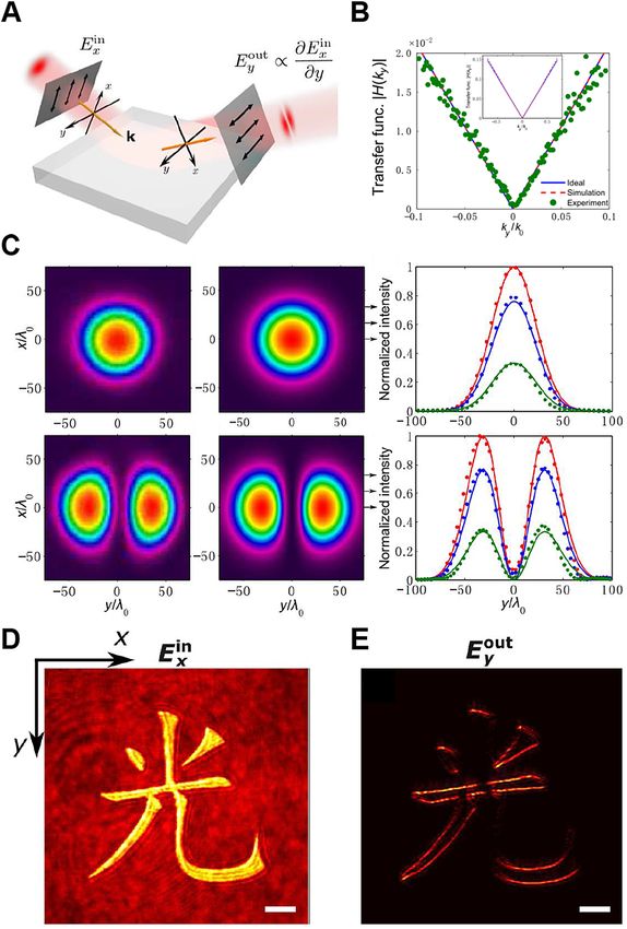
4078           S. Abdollahramezani et al.: Meta-optics for spatial optical analog computing

                                                                       Fourier transform (GRIN(+)) and inverse Fourier trans-
                                                                       form (GRIN(−)) subblocks, 2D GRIN media characterized
                                                                       by length Lg, unit relative permeability (i.e., μr = ±1), and
                                                                       parabolic-shaped permittivity, defined as ϵy  ±ϵc [1 −
                                                                       (π/2Lg )2 y2 ], with positive and negative sign for Fourier
                                                                       and inverse Fourier transform, respectively, are consid-
                                                                       ered. For the intermediate subblock (i.e., spatial Fourier
                                                                       filter), either a planar thin metamaterial with trans-
                                                                       versally inhomogeneous optical properties ϵmm (y)/ϵ0
                                                                       μmm (y)/μ0 or a transmitarray of metasurfaces, which
                                                                       consists of composite plasmonic–dielectric nanobricks
                                                                       [35], can be used. The transmitarray of metasurfaces is
                                                                       wisely engineered to encode the desired phase and
                                                                       amplitude patterns into the transmitted wave while
                                                                       minimizing disturbing reflections, which is necessary for
                                                                       highly efficient implementation of any desired local
                                                                       transfer function. Different mathematical operations
                                                                       were explored including first- and second-order differ-
                                                                       entiation, integration, and convolution. For the sake of
                                                                       brevity, we limit the discussion to the first-order spatial
                                                                       derivation.
                                                                             Considering the thickness of the planar metamaterial
                                                                       as Δ < λ0, where λ0 is the free-space wavelength of the
                                                                       infrared light, the relative permittivity and permeability
                                                                       associated with the normalized transfer function,
Figure 2: Metamaterials for spatial analog computing [34].             i.e., H(y) ∝ iy/(W/2), is described as follows [34]:
(A) Cascaded properly designed GRIN(+)/metastructure/GRIN(−)
                                                                                    ϵmm y μmm y      λ0    −iW
system to perform mathematical operations in the spatial Fourier                                    i    ln    .             (4)
domain. Two designs are proposed for the middle metastructure                         ϵ0      μ0        2πΔ     2y
including (i) a specific-purpose thin (Δ = λ0/3) single-layer
metasurface with the prescribed permittivity and permeability (left    Figure 2B illustrates the field distribution evolution
inset) and (ii) a general-purpose transmitarray of metasurfaces (so-   (snapshot in time) as the wave propagates through the
called metasurface transmitarray or MTA) comprising three              computational system. Comparison of the simulated elec-
metasurfaces formed by an array of hybrid plasmonic–dielectric         tric field distribution at the output plane (2Lg + Δ) and the
nanocubes that provide a rich set of transmission amplitude and
                                                                       first-order spatial derivative calculated analytically, given
phase profiles. A snapshot on the evolution of the z-component of
the electric field through the system operating as the first-order
                                                                       that the input function is f (y) ∝ exp( −y2 ), corroborates
differentiator formed based on (B) the first scenario (i.e., i) and     the performance of this approach. As a more practically
(C) second scenario (i.e., ii). Simulation results (both real and      feasible approach, the authors leveraged a transmitarray of
imaginary parts) are compared with the analytical solutions in the     metasurfaces cascaded with two GRIN(+) media to imple-
insets. GRIN, graded-index.                                            ment the first-order spatial derivation. Figure 2C represents
                                                                       the comparison assessment between numerical simula-
proper discretization in finite steps of the phase and                  tions and analytical results.
amplitude of the transfer function and assigning the                        To achieve strongly independent phase and amplitude
appropriate elements of the metasurface to encode the                  modulation, Pors et al. [36] utilized the rich nature of gap
transmission or reflection of the incident field. In what                surface plasmon mode in a plasmonic metareflectarray. As
follows, different frameworks for hardware implementa-                 shown in Figure 3A, their proposed structure consists of an
tion of the desired transfer function are discussed in detail.         array of gold (Au) nanobricks on a metal substrate sepa-
     In a seminal work, Silva et al. [34] proposed to use a            rated by an oxide spacer layer. Such a confined mode
system comprising three cascaded subblocks of Fourier                  excited in the gap between the top metallic nanoresonator
transform, an inhomogeneous spatial Fourier filter, and                 and the substrate propagates back and forth between the
inverse Fourier transform. As shown in Figure 2A, for the              two ends of the nanoresonator leading to the energy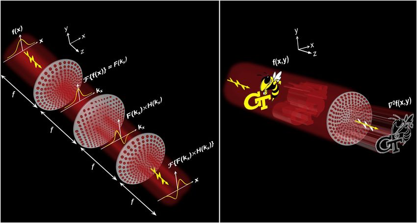
S. Abdollahramezani et al.: Meta-optics for spatial optical analog computing   4079

                                                                           generation highly miniaturized computational circuits.
                                                                           Motivated by that, Abdollahramezani et al. [37] recently
                                                                           introduced the concept of “metalines” that endows full
                                                                           control over the amplitude and phase profiles of the
                                                                           propagating graphene plasmons in a dynamic fashion. As
                                                                           shown in Figure 4A, a transmitarray of such metalines,
                                                                           whose surface conductivity can be locally and indepen-
                                                                           dently controlled through height encoding of the substrate
                                                                           beneath the graphene layer (or equivalently an external
                                                                           bias), enables realization of any transfer function in an
                                                                           ultrathin, integrable, and truly planar platform. Due to the
                                                                           high confinement of graphene plasmons that empowers
                                                                           the integration of the Fourier transform subblock in a
                                                                           cascaded structure, the presented 2D configuration is
                                                                           orders of magnitude smaller than the traditional
                                                                           metasurface-based counterparts. To facilitate the calcula-
                                                                           tion of surface conductivity–dependent transmission/
                                                                           reflection coefficients (Figure 4B) of the piecewise constant
Figure 3: Reflective plasmonic metasurfaces for spatial analog             elements of the dynamic metaline, the authors leveraged a
signal processing [36].
                                                                           representative simplified analytical treatment on the scat-
(A) Color map of the calculated reflection coefficient as a function of
                                                                           tering of graphene plasmons from inhomogeneous
the width of nanobricks for a reflective metasurface comprising an
array of Au nanobricks on top of an Au substrate separated with a thin     lateral hetrostructures. Figure 4C represents a comparison
oxide layer. Green curves indicate two contours of reflection phase        assessment of the computational system (i.e., GRIN lens/
with π-phase difference. (B) Position-dependent reflection amplitude/      transmitarray of metalines/GRIN lens) designed to perform
phase profile (top panel) and the corresponding nanobrick width            the second-order spatial derivation upon excitation with a
(bottom panel) for a 50-μm-wide differentiator and integrator. (C)
                                                                           beam with Sinc profile.
Bright-field images and the measured average normalized reflectivity
from the metasurface realizing the transfer function of differentiation         To harness the full potential of plasmonic and
(top panel) and integration (bottom panel). (D) Reflected far-field        dielectric modes within a single structure, Chizari et al.
intensity (top panel) and intensity profile averaged along the central     [38] proposed to use a metasurface comprising an engi-
part in the y-direction as a function of the x-coordinate (bottom panel)   neered array of size-variant nanoresonators on top of
for the differentiator (left panel) and the integrator (right panel)
system. Here, the excitation is through a bulky optical lens acting
                                                                           a silver (Ag) backreflector separated with an oxide inter-
as Fourier and inverse Fourier subblocks simultaneously.                   mediate layer (see Figure 5A). The combination of low-
                                                                           aspect ratio rotating silicon (Si) nanobricks, which sup-
                                                                           port the low-loss Mie resonance, and the lossy back-
leakage to free space. Strong modulation granted by such a
                                                                           reflector, which facilitates multiple reflections within the
Fabry–Perot-like resonance within the engineered inclu-
                                                                           low index spacer layer, grants unique agility on the
sion facilitates manipulation of the scattered near-infrared
                                                                           required phase delay and amplitude modulation of the
light both spectrally and spatially. As shown in Figure 3B
                                                                           cross-polarized light. As shown in Figure 5B, the designed
and C, it is evident that the fabricated computational
                                                                           unit cell can impart full 2π phase coverage corresponding
metasurfaces fairly follow the features of their designed
                                                                           with the desired amplitude in the range of (0, 1) on the
transfer functions while discrepancies exist in the spatial
                                                                           reflected near-infrared light. For the full operation, such a
variation of the reflectance due to mainly fabrication tol-
                                                                           compact design only needs one coupled lens serving as
erances, uncertainty in the material optical properties, and
interference of high-spatial frequencies reflected from the                 both Fourier and inverse Fourier transform subblocks
bare substrate. Hence, the proof-of-concept demonstration                  simultaneously. Figure 5C shows that a good agreement is
of the differentiator and integrator is not in very good                   achieved between the numerical simulation results and
agreement with the numerical calculations as depicted in                   the designed first-order differentiator and integrator us-
Figure 3D. However, this work is the first experimental                     ing such a complementary metal-oxide-semiconductor
implementation in the field of computational meta-optics.                   (CMOS)-compatible metasurface.
    Shrinking the conventional bulky 4f correlator to on-                       While the reflective plasmonic metasurfaces generally
chip integrable configurations is highly desirable for next-                provide larger phase span thanks to the added Fabry–Perot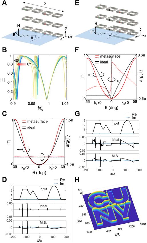
4080           S. Abdollahramezani et al.: Meta-optics for spatial optical analog computing

                                                                       demonstrated that an all-dielectric metasurface based on an
                                                                       array of anisotropic Si nanoresonators can fully tailor the
                                                                       transmission amplitude and phase responses locally and
                                                                       almost independently (see Figure 6A), which can facilitate
                                                                       the realization of mathematical operators. Such a unique
                                                                       feature is granted by the magnetic dipole moment on ac-
                                                                       count of the circular displacement current excitation and
                                                                       the electric dipole moment due to considerable charge
                                                                       accumulation at the corner of each resonator (see
                                                                       Figure 6B). Thanks to the the interplay between the first and
                                                                       second Mie resonant modes (i.e., magnetic and electric
                                                                       dipole moment) achieved by changing the major-to-minor
                                                                       axis aspect ratio of the nanoresonator, fairly any desired
                                                                       transformation of the amplitude and phase can be imparted
                                                                       on the transmitted light (see Figure 6A). The authors lever-
                                                                       aged the full potential of a cascaded, compact platform of
                                                                       metalens/computational metasurface/metalens to perform
                                                                       all-optical signal processing including constant coefficient
                                                                       integrodifferential equation (see Figure 6C and D), which
                                                                       has not been shown previously. Taking advantage of the
                                                                       incorporated metalenses as the functional Fourier and in-
                                                                       verse Fourier transform subblocks, rather than the bulky
                                                                       conventional lenses, paves the way for highly integrable on-
                                                                       demand computational systems.
                                                                            Considering well-established foundry-based silicon
                                                                       photonics, implementation of on-chip mathematical op-
                                                                       erators promises the next generation of small footprint,
                                                                       low-power consumption, and multipurpose computational
                                                                       photonic integrated circuits. More recently, Wang et al. [40]
                                                                       demonstrated parallel signal processing by leveraging a 1D
Figure 4: Linear transversely invariant graphene-based                 on-chip high-contrast transmitarray of metasurfaces (see
metastructure to perform mathematical operations [37].
                                                                       Figure 7A). By judiciously adjusting the width and length of
(A) Sketch of a two-dimensional (2D) graphene-based computing
                                                                       the void slots in the Si-on-insulator substrate, complete
system consisting of two cascaded graded-index (GRIN) lenses
incorporating a transmitarray of three symmetric stacked metalines     control of the transmitted amplitude and phase profile can
with total length of D and width of W (inset: basic unit cell of the   be achieved over a high bandwidth (see Figure 7B).
metaline). (B) Transmission phase and amplitude of the metaline as     Figure 7C illustrates experimental results of the fabricated
a function of the chemical potential associated with the surface       three-layer system necessary for successful implementa-
conductivity. (C) Snapshots of the z-component of the electric field
                                                                       tion of on-chip mathematical operators. While the first and
distribution through the GRIN lens/transmitarray of metalines/GRIN
lens system as a second-order differentiator given that the input      second metalenses perform the Fourier and inverse Fourier
wave is a Sinc function.                                               transform, the spatially varying transmission coefficient is
                                                                       encoded into the middle mask layer to perform the required
                                                                       1D transfer function (see inset in Figure 7C). The calculated
channel, transmittive metasurfaces grant easy access to the            analytical, numerically simulated, and measured spatial
processed field profile at their output, which is a must for           spectra are in good alignment for the spatial differentiator
cascadable optical systems. However, optical metasurfaces              as shown in the bottom panel of Figure 7C. Exploiting an
supporting plasmonic resonances exhibit intrinsic non-                 integrated metalens (shown in Figure 7D) significantly
radiative losses and limited scattering cross sections.                miniaturizes the overall size of the on-chip photonic
To mitigate these challenges, high-contrast metasurfaces               processor.
have recently garnered significant attention in the field of                More recently, Zhou et al. [41] have shown experi-
nanophotonics. Abdollahramezani et al. [39] recently                   mental realization of first-order spatial differentiation and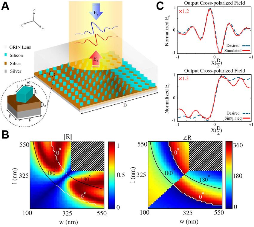
S. Abdollahramezani et al.: Meta-optics for spatial optical analog computing   4081

                                                                         implemented right after the metasurface), only two shaded
                                                                         areas are left at the output that indicate the edges of the
                                                                         input image. The fabricated metasurface with 8 mm × 8 mm
                                                                         pattern area embedded inside a 3-mm-thick glass substrate
                                                                         is shown in Figure 8F. The metasurface pattern is written by
                                                                         a femtosecond pulsed laser beam focused 50 μm beneath
                                                                         the surface of the glass. Interestingly, this edge detection
                                                                         technique enables tunable resolution at the resultant edges
                                                                         by varying the PB phase gradient period. Moreover, as
                                                                         shown in Figure 8G, this edge detection technique is sen-
                                                                         sitive to the orientation of the phase gradient metasurface
                                                                         (i.e., the gradient direction of the 1D metasurface indicated
                                                                         by white arrows). The use of thick glass-based meta-
                                                                         structure in their implementation makes the metasurface
                                                                         highly efficient in terms of transmitted power (around
                                                                         90%) which is the main advantage over the plasmonic
                                                                         metasurfaces. Additionally, since the operational band-
Figure 5: Analog optical computing using hybrid dielectric–
                                                                         width of this approach is not limited by the critical plas-
plasmonic metasurfaces [38].
(A) Schematic representation of the dielectric graded-index (GRIN)
                                                                         monic coupling condition [42], realization of broadband
media/hybrid metasurface to perform mathematical operations              transfer functions is guaranteed. An interesting extent of
including spatial differentiation and integration. The metasurface is    this work can be implementation of a broadband highly
composed of an arrangement of silicon (Si) nanobricks on an oxide        efficient 2D edge detector.
layer deposited on a silver (Ag) substrate. (B) Simulated amplitude
                                                                               In addition to so far demonstrated platforms enabling
and corresponding phase profiles of the reflected cross-polarized
light considering the rotation angle of 45° with respect to the x-axis   mathematical operators, several other theoretical works
for the constituent nanoresonator. (C) Comparison of the simulated       exist in the literature using spatial Fourier transformation
reflected cross-polarized field and the exact analytical solution for      concept to realize first-order differentiation using bilayered
the first-order differentiator (top panel) and first-order integrator      metasurfaces [43], differential and integral operations
(bottom panel).
                                                                         using Ag dendritic metasurfaces [44, 45], and multiway
                                                                         parallel mathematical operations based on discrete meta-
demonstrated broadband 1D edge detection by leveraging
                                                                         materials [46].
the spin–orbit interaction of light and a properly designed
Pancharatnam–Berry (PB) phase metasurface sandwiched
between two orthogonally aligned laser-written linear Glan
polarizers. The PB phase gradient metasurface splits the                 3 Green’s function approach
incident linearly polarized (LP) beam into left-handed
circularly polarized (LCP) and right-handed circularly                   In the GF approach, the desired optical transfer function is
polarized (RCP) beams propagating in opposite directions                 directly implemented into the wave vector domain (Fourier
(see Figure 8A). To explore the effectiveness of the pro-                or k-space) by using the nonlocal (angular dependent)
posed approach, the edges of a squared-shaped object (slit)              response of a suitably designed metamaterial or metasur-
are detected in an analog fashion. The real-space image                  face as shown in Figure 1B [47–51]. Due to the direct
(i.e., the electric field distribution of the object in the spatial       implementation of the desired transfer function in this
domain) and the Fourier space spectrum of the object are                 method, performing Fourier/inverse Fourier transforms is
shown in Figure 8C and B, respectively. By introducing a                 no longer needed, which in turn leads to the reduction in
PB phase gradient metasurface at the Fourier plane (see                  the overall structure size [34]. On the other hand, it can be
Figure 8D), the LCP and RCP components of the output                     very difficult to realize a desired but arbitrary complex
electrical field at the image plane obtain opposite phase                 transfer function in the GF approach. Here, we present a
gradients. This, in turn, results in a slight shift of LCP and           general 2D description of the GF approach which can be
RCP images in opposite directions as shown in Figure 8E.                 simplified into a 1D description as described later in this
When this output image passes through the analyzer                       section. First, assume that a field component of a mono-
(i.e., the orthogonal Glan polarizer along y-direction                   chromatic beam propagating in the +z direction is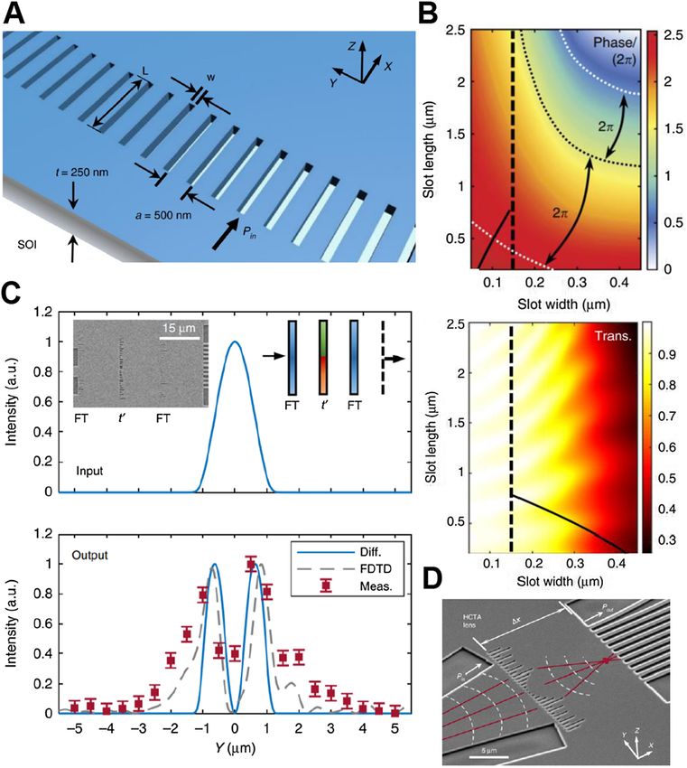
4082             S. Abdollahramezani et al.: Meta-optics for spatial optical analog computing

                                                                                   can be represented as an optical transfer function (OTF)
                                                                                   denoted by the following equation [53]:

                                                                                                             H TE−TE k x , k y  H TE−TM k x , k y
                                                                                         Hk x , k y                                                .    (5)
                                                                                                             H TM−TE k x , k y  H TM−TM k x , k y

                                                                                        The OTF tensor H(k x , k y ) can transform the incident field
                                                                                   profile to a reflected or transmitted field profile. The manip-
                                                                                   ulation of the geometry of the structure representing the
                                                                                   H(k x , k y ) allows for designing the on-diagonal elements
                                                                                   (couplingofparallelpolarizations)andoff-diagonalelements
                                                                                   (coupling of orthogonal polarizations) in Eq. (5). It should be
                                                                                   notedthat inthis formulation, only the zeroth-order reflection
                                                                                   and refraction are considered to occur. The elements of the
                                                                                   OTF of a certain structure can be calculated using numerical
                                                                                   simulation methods such as the finite element method of
                                                                                   finite difference time domain [53]. By simply multiplying the
                                                                                   incident field profiles with the OTF of a structure, one can
                                                                                   obtain the transmitted or reflected field profile of the corre-
                                                                                   sponding output plane waves as follows [53]:

                                                                                                GTE k x , k y                       F TE k x , k y
                                                                                                                   Hk x , k y                      .   (6)
                                                                                                GTM k x , k y                       F TM k x , k y
Figure 6: All-dielectric metasystems as equation solvers [39].
(A) Numerically calculated phase and amplitude of transmitted light
from the computational metasurface as a function of minor and
                                                                                        To design the tailored structures for realization of the
major axis dimension. (B) Simulated electric and magnetic lines in                 desired OTFs, different optical phenomena have been
the cross section of a silicon (Si) nanodisk at the electric and                   used. Here, we classify them into two main categories as
magnetic resonances fulfilled at structural parameters associated                  resonance- and nonresonance-based optical phenomena.
with the dots shown in (A). (C) Snapshot of the y-component of the
                                                                                        As a leading work, Silva et al. [34] investigated optimized
simulated electric field propagating through the computational
metasurface realizing the kernel for solving the
                                                                                   multilayered metamaterial slabs, which are homogeneous in
integrodifferentiation equation.                                                   the transverse directions while inhomogeneous in the lon-
(D) Comparison assessment between the normalized electric field at                 gitudinal direction, to realize an appropriate GF associated
the output of the proposed metalens/computational metasurface/                     with the second-order spatial derivation. A fast synthesis
metalens system and analytical results for integrodifferential
                                                                                   method to calculate the corresponding optical constant and
equation solving.
                                                                                   thickness of parallel subwavelength layers was developed.
                                                                                   The ten-layer nonmagnetic metamaterial in Figure 9A is
                                                                                   designed to manipulate the transmission coefficient to match
modulated by an arbitrary 2D signal profile f(x, y). This field                      the second-order derivative kernel for any incidence angle.
profile can be decomposed into transverse electric (TE) and                         Figure 9B and C demonstrate the evolution of magnetic field
magnetic (TM) linearly polarized plane waves when rep-                             distribution and the simulation results at the output of the
resented in the wave vector space. Through Fourier trans-                          multilayered slab upon excitation with a nonregular poly-
form, one can obtain the complex amplitude of each of                              nomial function and a city skyline border, respectively.
these plane wave components, i.e. F TE (k x , k y ) or                             Figure 9D shows the simulation results for a five-layer GF
F TM k x , k y . It is noteworthy that F TE (k x , k y ) and F TM k x , k y    slab characterized by a rectangular spatial kernel performing
can be obtained only by knowing the transverse compo-                              convolution operation of a rectangular function.
nents of the electric field. One can calculate other field
components using Maxwell’s equations as described in the
study by Bykov et al. [52]. The next step is to judiciously                        3.1 Resonance-based GF approach
design an optical structure that properly manipulates the
amplitude and phase of each of the decomposed TE and TM                            Different types of optical resonances such as Fano reso-
plane wave of the incident field profile. The application of                         nance [16, 54, 55], surface plasmon resonance, and guided
such a desired amplitude and phase on these plane waves                            mode resonance (GMR) have been utilized for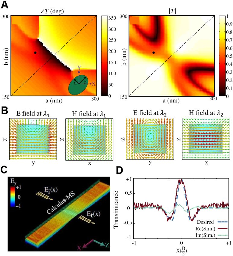
S. Abdollahramezani et al.: Meta-optics for spatial optical analog computing   4083

                                                                          theory, the authors in the study by Zhu et al. [42] showed
                                                                          that the OTF of this structure around kx = 0 and under
                                                                          critical coupling condition (achieved by simply controlling
                                                                          the thickness of the metal film) can be approximated as
                                                                          follows:

                                                                                               HTM (k x ) ≈ eiϕ ik x   B             (7)

                                                                          in which ϕ corresponds to the phase change during the
                                                                          direct reflection at the glass–metal interface, and B is
                                                                          expressed in terms of the radiative leakage rate of the SPP
                                                                          and the intrinsic material loss rate, showing that the
                                                                          structure in Figure 10A can perform first-order derivative
                                                                          for off-normal incidence (i.e., θ0 ≠ 0) as shown in
                                                                          Figure 10B. Given that a first-order differentiator is able to
                                                                          map the abrupt changes in the spectrum (either amplitude
                                                                          or phase) of a input signal to some sharp peaks in an output
                                                                          signal, the authors in the study by Zhu et al. [42] experi-
                                                                          mentally demonstrated 1D edge detection of the input
                                                                          Stanford logo image as shown in Figure 10C.
                                                                               To broaden the operational spatial bandwidth for on-
                                                                          demand high-resolution edge detection, Kwon et al. [50]
Figure 7: On-chip analog computing based on a Si-on-insulator             proposed to use a high-efficiency transmittive metasurface
(SOI) platform [40].                                                      consisting of a periodic array of split-ring resonators (SRRs)
(A) Schematic representation of an on-chip high-contrast
                                                                          as demonstrated in Figure 11A. They theoretically showed
transmitarray defined on a SOI substrate to manipulate the
transmittance and phase response of the in-plane propagating              that by introducing a periodic (sinusoidal) permittivity
wave. (B) Simulated amplitude (top panel) and phase (bottom panel)        modulation in SRR gaps, the nonlocal response of the
spectra of the transmitted field as functions of the slot width (w) and   metasurface can be engineered to achieve desired OTFs for
height (h) for an incident wavelength of 1550 nm. Contours with 2π        the second-order differentiator. The interaction of the
phase shift are depicted by dotted lines. (C) The input incident wave
                                                                          surface GMRs with the leaky-wave resonances can lead to
profile (top panel) and analytical, simulated, and measured
distribution at the output (bottom panel) of the on-chip                  some Fano resonances in the transmission response of this
differentiator. The conceptual design and scanning electron               metasurface as shown in Figure 11B. Working at the
microscopy (SEM) of the fabricated device are shown in the inset. (D)     transmission zero frequency of the Fano resonance at
SEM of the fabricated on-chip metalens located in front of a mode         normal incidence, the transmission response of the
expander and coupled to 11 single-mode waveguides to facilitate
                                                                          nonlocal metasurface changes from zero to unity for obli-
characterization of the spatial distribution of focused light.
                                                                          que incidence (see Figure 11C). This functionality can be
implementing OTFs to perform mathematical operations in                   utilized for performing wide bandwidth second-order dif-
wave vector domain.                                                       ferentiation as shown in Figure 11D. They also modified this
    In 2017, Zhu et al. [42] experimentally demonstrated a                structure by adding a misplaced array of metallic wires to
surface plasmon–based spatial differentiator using a sim-                 break the vertical and horizontal mirror symmetry (see
ple metal–dielectric plasmonic structure in the reflective                 Figure 11E). Such a suitably engineered configuration en-
Kretchmann prism configuration as shown in Figure 10A.                     ables realization of the first-derivative kernel as shown in
They showed that when the parallel component of the                       Figure 11F. Figure 11G represents the input signal and the
TM-polarized incident wave to the interface matches with                  corresponding simulated response of this mathematical
the wave vector of the surface plasmon polariton (SPP) at                 operator in comparison to the numerically calculated
the metal–air interface, a strong SPP is excited and prop-                result. In a further study, by integration of two identical 1D
agates along the metal surface. The interaction between                   operation metasurfaces relatively rotated by 90°, which
the radiation of the SPP leakage with the direct reflection                implies 90° rotational symmetry, such a configuration
from the glass–air interface determines the amplitude of                  enabled realization of an identical second-order derivation
the reflected beam and, in turn, the OTFs of the structure.                for TM-polarized waves along the x and y axes. This plat-
Considering this mechanism and using coupled mode                         form can be leveraged for more practical 2D edge detection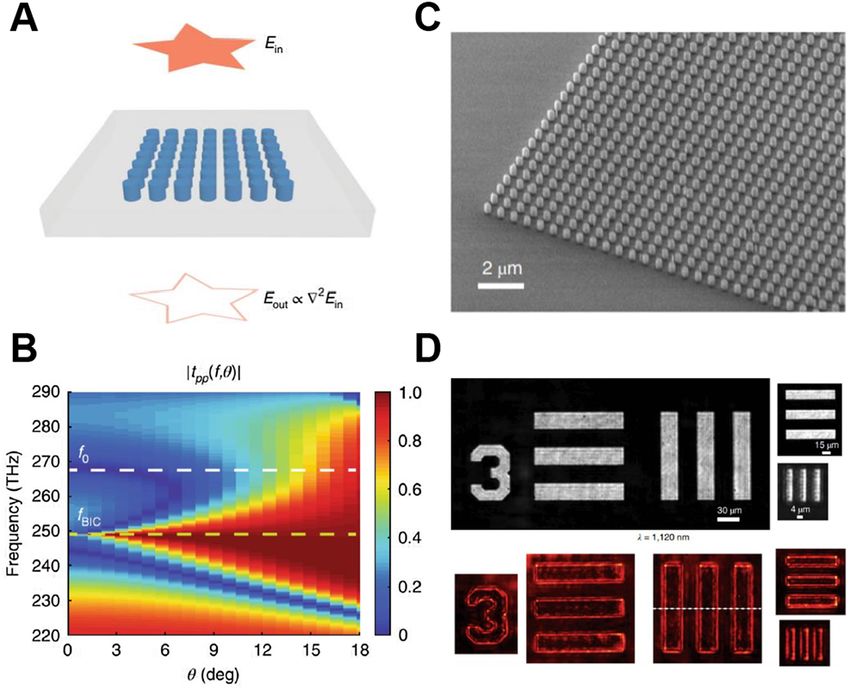
4084            S. Abdollahramezani et al.: Meta-optics for spatial optical analog computing

                                                                          beam. GMRs have also used for implementing optical in-
                                                                          tegrators. The authors in the study by Zangeneh-Nejad and
                                                                          Khavasi [60] utilized a prism coupling configuration to
                                                                          implement the OTF of a 1D optical integrator in the trans-
                                                                          mission response of a multilayer dielectric slab structure. It
                                                                          is shown that the dielectric slabs can be replaced by gra-
                                                                          phene sheets to enable miniaturized optical integrator.
                                                                               In another work, Guo et al. proposed to use a photonic
                                                                          crystal slab (see Figure 12A) in the transmission mode to
                                                                          realize the Laplacian operation on a 2D input, i.e.
                                                                          ∇2  ∂2x + ∂2y . The ∇2 operation in real space is equivalent to
                                                                          the following OTF [56]:

                                                                                                     T TE−TE k x , k y         0
                                                                                 Hk x , k y                                                .   (8)
                                                                                                             0            T TM−TM k x , k y

Figure 8: Edge detection using Pancharatnam–Berry (PB) phase                   To realize this ideal 2D Laplacian operation, the au-
gradient metasurfaces [41].                                               thors in the study by Guo et al. [56] utilized the guided
(A) The concept of PB phase. Upon illumination of an incident
                                                                          modes of the photonic crystal slab near the Γ point in the
linearly polarized (LP) beam, the PB phase metasurface splits the
light into left-handed circularly polarized (LCP) and right-handed
                                                                          Brillouin zone, and the authors in the study by Guo et al.
circularly polarized (RCP) beams with opposite directions. The            [62] used isotropic image filters to have identical responses
Fourier space spectrum (B) and real-space image (C) of a square           to both polarization and make the off-diagonal elements
object. When a PB phase gradient metasurface is added at the              equal to zero as required by Eq. (8). It is worth mentioning
Fourier plane, (B) and (C) change to (D) and (E), respectively. (F) The   that working in the transmission mode is more compatible
fabricated metasurface with a pattern area of 8 × 8 mm embedded in
                                                                          for image processing applications which is an advantage of
a 3-mm-thick glass substrate (scale bar is 5 mm). The polariscope
optical image of the area marked in the left panel is shown in the        the work in the study by Guo et al. [56] over other ap-
right panel (scale bar is 25 μm). The constituent elements in one         proaches for Laplace operator implementation [52]. The
period of the metasurface are indicated by the red bars in the right      numerical demonstration of the proposed structure shown
panel, and the inset shows the SEM of the fabricated device (scale        in Figure 12A is demonstrated in Figure 12B, where the
bar is 500 nm). (G) The top left panel shows the original image, while
                                                                          transmitted image of an unpolarized incident beam of the
other three panels show detected images at the output of the
system. Different orientation of the intermediate metasurface,            Stanford emblem, as well as some slot patterns, is calcu-
which is indicated by the white arrows, resolves different portion of     lated. Later, Bezus et al. [63] employed the resonance of a
edges.                                                                    dielectric ridge on a slab waveguide to implement both
                                                                          optical differentiation and integration in the spatial
                                                                          domain.
scenarios where unpolarized light for the illumination of                      Zhou et al. [61], more recently, demonstrated the
the image is utilized as depicted in Figure 11H where the                 applicability of flat optics for direct image differentiation
edges of the City University of New York (CUNY) logo are                  using a compact all-dielectric metastructure. In their work,
well resolved.                                                            first a metasurface-based differentiator was used in com-
    The authors in the study by Saba et al. [57] employed the             bination with the conventional optical components and a
GMR of a periodic array of dielectric resonators buried in a              camera sensor for high-speed edge detection (see
dielectric slab to perform 2D edge detection. The interaction             Figure 13A). Such a metasurface affords a improved
between the GMRs with the leaky waves of the structure                    transmission amplitude profile as shown in Figure 13B. In a
results in some Fano resonances in the transmission                       second approach, a Si-based photonic crystal in combi-
response [58]. Working at the zero transmission corre-                    nation of a metalens was employed to realize the second-
sponding to the normally incident light, the authors                      order derivation to directly discriminate edges in an image
numerically demonstrated a second-order differentiator                    (see Figure 13C). Such a compact and monolotic image
owing to the even symmetry of the structure. In another                   processing system paves the way for real-time computer
work, the authors in the study by Bykov et al. [59] experi-               vision tasks, as depicted in Figure 13D.
mentally demonstrated a first-order differentiator by                           In a follow-up work to the study by Kwon et al. [50],
employing GMRs in the case of an oblique incident Gaussian                Cordaro et al. [49] designed and implemented an all-
S. Abdollahramezani et al.: Meta-optics for spatial optical analog computing 4085
Figure 10: (A) The structure of a surface plasmon-based first-order
spatial differentiator consisting of a Ag film on top of the glass in the
Kretschmann configuration [42]. (B) The first-order spatial differ-
entiator optical transfer function (OTF) obtained by the experimental
measurement (dotted lines) and the numerical fitting (solid lines).
(C) Edge detection of the Stanford tree logo and the letters as the
incident image (left panel) using the plasmonic structure shown in
(A). The reflected intensity image is shown in the right panel.
Several other proposals and demonstrations using
Figure 9: Spatial analog computing using metamaterial slabs based
on Green’s function approach [34].
spin Hall effect (SHE) of light [65], prism coupling config-
(A) Designed multilayered slab to realize the desired Green’s uration [66], reflective hybrid plasmonic–dielectric meta-
function (GF) kernel corresponding to the selected mathematical surfaces [48], periodic plasmonic metasurfaces covered by
operation. Evolution of electromagnetic wave in the ten-layered graphene [67], multiinput–multioutput computational
nonmagnetic GF slab designed to perform second-order metasurfaces [68], ultrathin bianisotropic metasurfaces
differentiation on a quadratic polynomial function (B) and a city
[69], polarization-insensitive structured surfaces with
skyline (C). In (C), the simulated output result is directly compared
with the input function to highlight the performance of the system in tailored nonlocality [70], and engineering the spatial
detecting sharp edges. (D) GF slab with five layers designed to dispersion of the electric dipole resonance in dielectric
realize convolution with a rectangular kernel. metasurfaces [71] to perform mathematical operators based
on GF approach have been reported in the literature.
dielectric metasurface formed by a 1D array of Si nano- 3.2 Nonresonance-based GF approach
beams to locally tailor the optical properties of the incident
S-polarized light. Due to engineered spatial dispersion, the The authors in the study by Youssefi et al. [64] employed
interference of the broad Fabry–Perot resonance of struc- the Brewster effect, which is associated with the zero
ture with the quasi-guided mode along the surface results reflection of a TM-polarized incident beam from an inter-
in an asymmetric Fano resonance in the transmission mode face between two dielectric medium, to realize first-order
shown in Figure 14A. The sharp response in frequency is differentiation. The schematic of their proposed structure is
associated with strong nonlocality governing the angular shown in Figure 15A in which the symmetry of the system is
sensitivity of the transmission response. The strong broken by applying oblique incident beam. Figure 15B
amplitude modulation correlated to the incoming k-vector shows the exact GF and its approximation around ky = 0
is the basis for implementing a spatial filter associated with which can be used for implementation of first-order de-
the mathematical operator of choice. The simulated rivative. To study the performance of the proposed
transmission amplitude and phase as a function of the configuration, the proposed structure is illuminated with a
normalized in-plane wave vector for the second-order dif- Sinc function beam profile with the bandwidth of
ferential kernel at the operational wavelength of 633 nm is W = 0.09k0 at the Brewster angle. The calculated first-order
shown in Figure 14B. Figure 14C shows the results of the derivative of the input field is compared with the exact
simulated metasurface; a rectangular input profile results solution as shown in Figure 15C. Later, the same group
in doublet signals at the edges of the rectangle, and the demonstrated that using a simple half-wavelength dielec-
sinusoidal input function results in the sinusoid becoming tric slab in the reflection mode, first-order differentiation
flipped. can be realized [72]. Using a transmission-line approach,4086 S. Abdollahramezani et al.: Meta-optics for spatial optical analog computing
or refracted at a single optical planar interface under par-
axial approximation. They employed SHE of light, i.e. the
polarization-dependent transverse shift of an optical beam
totally reflected from a planar interface [73], to compute the
spatial differentiation of the incident beams. As Figure 16C
shows, when the obliquely incident paraxial beam has an
electric field distribution of f(x, y), the output field distri-
bution associates with df (x, y)/dy. To validate their
finding, the authors in Zhu et al. [65] performed experi-
mental measurements of the OTF of a glass–air interface as
shown in Figure 16C. Moreover, they applied their method
to a Gaussian incident beam profile and performed the first-
order spatial differentiation as the first-order Hermite–
Gaussian profile of the reflected beam in Figure 16C shows.
Finally, they applied their spin-optical method to perform
an edge detection operation. Figure 16D demonstrates the
incident image field of a Chinese character encoded in the
x-component of the field based on the amplitude modula-
tion. The measured y-component of the reflected field ex-
hibits the resolved outlines of the character (see Figure 16E)
which are more visible in the x direction. The edges parallel
to the x direction are more visible since the differentiation
is performed along the y direction.
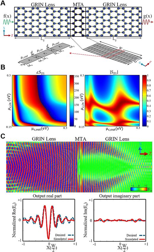
More recently, Estakhri et al. [74] in a disruptive
approach demonstrated a computational metastructure
platform that solves linear integral equations by tailoring
the complex-valued electromagnetic wave propagating
through the specially designed recursive paths. The con-
ceptual representation of the metastructure is shown in
Figure 17A where the solution to the Fredholm integral
equation of the second kind is obtained. While the given
Figure 11: Nonlocal metasurface. integral operator with kernel K(u, v) is implemented in the
(A) The structure of a metasurface consisting of an array of split-ring metamaterial block, the input signal Iin(u) is introduced
resonators (SSRs) under TM illumination [50]. (B) The spectrum of to the equation through a set of coupling elements
the transmission response of the metasurface when SSRs are
along the feedback waveguides. The overall relation
periodically modulated. (C) The optical transfer function (OTF) if the
metasurface fitted to a second-order differentiator. (D) Output of an describing the behavior of the equation solver follows
b
ideal second-order differentiator and of the metasurface from the g(u) I in (u) + ∫a K(u, v)g(v)v, in which g(u) is the un-
input signal shown in the top panel. (E) Broken-symmetry
metasurface enabling an asymmetric response with respect to
known solution of the integral equation. To realize the
positive and negative kx to realize first-order differentiation. (F) The equivalent N × N matrix equation of the abovementioned
transmission profile as a function of the incidence angle for a governing equation, N feedback waveguides are exploited
symmetry-broken metasurface enabling first-derivative operation. to sample the input of the metamaterial block to its output.
(G) Output of an ideal first-order differentiator working as an edge
To showcase the performance of this approach in a phys-
detector. (H) Detected edges of the CUNY logo for illumination with
unpolarized light from the normal direction [50].
ical system, the authors leveraged a judiciously patterned
metastructure included in a feedback loop, which calcu-
lated the inverse of a known N × N matrix. Figure 17B shows
they showed that employing impedance matching condi- the numerical simulation results for the distribution of the
tion, one can perform first-order differentiation on oblique electric field in the assembled system consisting of the
incident input signals. prescribed metastructure in combination with the five
Recently, Zhu et al. [65] experimentally demonstrated feedback waveguides and directional couplers. The com-
spatial differentiation of the incident beam when reflected parison assessment between the theoretical andS. Abdollahramezani et al.: Meta-optics for spatial optical analog computing 4087
simulation results corroborate the fidelity of the proposed solution, as well as spatial frequency filters. Despite the
approach. In a proof-of-concept demonstration at the mi- existing promising platforms and design approaches
crowave regime, the feedback process is internally per- enabling computational metasystems, there is still room
formed in a reflective system, as shown in Figure 17C. The for improvement and progress in this rather infant field. In
topology optimization method was leveraged to inversely what follows, we elaborate some of unexplored aspects,
design an optimized metastructure realizing the kernel key challenges, and possible opportunities in the general
associated with the operator of choice. The simulated field of computational meta-optics.
electric field and comparison between the numerical and In general, the architecture of a conventional optical
experimental results are represented in Figure 17C. processor is relied on cascaded input, processing, and
output planes. To leverage the profound potential of meta-
optics for realization of flat optical processors, miniaturiza-
tion and possible stacking of planes are indispensable. The
4 Summary and outlook first (or input) plane, where mostly an electrical to optical
conversion of raw data is performed at the video rate using
Spatial analog computing platforms facilitate wave-based, an SLM, is considered to be the bottleneck of most practical
real-time, high-throughput, and large-scale information computational systems. More recently, several tuning
processing with low-energy consumption. Fourier trans- mechanisms including electrical, thermal, mechanical, and
formation and GF have been pursued as two powerful optical have been introduced [75] enabling reconfigurable
concepts for realization of mathematical operations. While nanoscale SLMs and phased array antennas. Tuning the
the former is relied on 4f systems with two Fourier trans- refractive index of Si based on thermooptic effects [76],
form lenses and one intermediate spatial frequency filter, manipulating the electrooptic characteristics of indium tin
the latter leverages the nonlocal response of judiciously oxide [77, 78] relying on free carrier effects, controlling the
designed optical components to implement the desired effective physical state of liquid crystals [79] exploiting the
kernel. Due to their unprecedented capabilities in sculpt- ultrafast transport dynamics of hot electrons in a hybrid
ing the scattered light, metastructures enable miniaturi- crystal [80], and phase conversion of phase change mate-
zation of traditional bulky optical systems to the integrable rials between the amorphous and crystalline states [81–89]
ultracompact frameworks. The intersection of the afore-
mentioned fundamental theoretical concepts and func-
tionalized metamaterials and metasurfaces promise
realization of computational meta-optics. We discussed
recent advances in spatial analog optical computing de-
vices enabling mathematical operations including inte-
gration, differentiation, and integrodifferential equation
Figure 13: Two-dimensional (2D) image differentiation using
Figure 12: (A) The schematic of the photonic crystal structure for nanophotonic materials [61].
Laplacian differentiation consisting of a photonic crystal slab (A) Schematic of a photonic crystal slab acting as a Laplacian
separated from a uniform dielectric slab by an air gap [56]. operator that transforms an image, Ein, into its second-order
(B) Incident Stanford emblem (top left panel) and calculated derivative, E out ∝ ∇2 E in . (B) Simulated color-coded transmission
transmitted image with unpolarized light (top right panel). The coefficient amplitude as a function of frequency and incident angle
spatial resolution of the differentiator is shown in the bottom panels along the Γ − X direction (ϕ 0°) for p polarization. (C) SEM of the
(incident slot patterns in the left and calculated transmitted images fabricated Si photonic crystal. (D) Imaging results for the target
with unpolarized light in the right). without (top row) and with (bottom row) the differentiator.You can also read