Light Industry Technology of Chiral Perovskite Nanomaterials Construction and Photoelectric Properties - Hindawi.com
←
→
Page content transcription
If your browser does not render page correctly, please read the page content below
Hindawi
Advances in Materials Science and Engineering
Volume 2021, Article ID 7965081, 10 pages
https://doi.org/10.1155/2021/7965081

Research Article
Light Industry Technology of Chiral Perovskite Nanomaterials
Construction and Photoelectric Properties

 Jie Sun
 Department of Construction Engineering and Office, Yantai Vocational College, Yantai 264670, Shandong, China

 Correspondence should be addressed to Jie Sun; 20140912@stu.nun.edu.cn

 Received 11 June 2021; Revised 20 August 2021; Accepted 25 August 2021; Published 21 September 2021

 Academic Editor: Song Jiang

 Copyright © 2021 Jie Sun. This is an open access article distributed under the Creative Commons Attribution License, which
 permits unrestricted use, distribution, and reproduction in any medium, provided the original work is properly cited.

 Perovskite nanomaterials have become a new research hotspot due to the many novel physical properties of quantum effects and
 have good application prospects in the field of optoelectronics. Among them, the realization of controllable fabrication of
 perovskite nanomaterials is the basis of performance studies and applications and is also a difficult point. Reducing production
 costs to improve manufacturing methods, further improve product controllability, promote advantages, or improve disadvantages
 will be very important for further application of perovskite nanomaterials. Therefore, this paper studies the construction of
 titanium ore nanomaterials by designing a novel preparation process and, at the same time, analyzes the related optoelectronic
 properties of the obtained materials. In this paper, a triangular PbI2 nanosheet having a uniform and controllable shape and size
 was successfully fabricated by physical vapor deposition through the introduction of a limited space, and related characterization
 was performed to show uniform controllability and high crystallinity. Using PbI2 nanosheets as the substrate, MAPbI3 nanosheets
 were further prepared and related characterizations proved that the obtained nanosheets had high crystallinity and excellent
 optical properties. The experiment proves that the peak position of the fluorescence spectrum obtained by Gaussian fitting is
 800 nm and the half-peak width is about 45 nm. At the same time, MAPbI3 exhibits strong light absorption characteristics when
 the wavelength is less than 800 nm. This shows that this enclosed space deposition method can improve the uniformity and
 controllability of PbI2 and MAPbI3 nanosheet fabrication, which provides the basis for further research on MAPbI3 nanomaterials
 and references to the controllable growth of other nanomaterials.

1. Introduction The study of the structure and optoelectronic properties
 of perovskite nanomaterials abroad is much faster than in
As a direct band gap semiconductor, perovskite has many China, the discovery of perovskite nanomaterials is also
advantages, such as designable structure, continuously ad- faster than in China, and the construction technology of
justable band gap, high light absorption and emission effi- nanomaterials is rapidly developing and updating. The
ciency, high carrier mobility, and low preparation cost. It has construction and optoelectronic properties of perovskite
become a star material that has attracted much attention. nanomaterials have been greatly improved and developed. It
When the perovskite is further made into nanomaterials, due is believed that the application of perovskite nanomaterials
to the quantum effect, it will exhibit many novel physical and in light industry will become more and more extensive in the
chemical properties, further expanding its application range. near future. Ha et al. synthesized a series of tantalate
Perovskites also have excellent electrical properties, high hole compounds with Dion–Jacobson layered perovskite struc-
mobility, and carrier diffusion lengths up to the millimeter ture by solid-phase method. These compounds can photo-
level. When perovskites form nanomaterials, they have newer catalytically decompose water to produce hydrogen and
properties due to quantum effects. Because of these out- oxygen under the irradiation of ultraviolet light [1]. Halford
standing optical and electrical properties, perovskites, espe- studied the Ruddlesden-Popper layered perovskite structure
cially perovskite nanomaterials, have been extensively studied. compound and found that it can effectively degrade

2 Advances in Materials Science and Engineering

rhodamine B solution under ultraviolet light irradiation and change with the thickness of perovskite nanomaterials [7, 8].
have a wide range of applications in photocatalytic sterili- From the single layer to the bulk phase, the bandgap offset
zation, water purification treatment, and conversion of solar can reach 100 meV, which shows that the thickness of the
energy to hydrogen energy [2]. Riba et al. prepared a series of perovskite nanosheets has a great influence on the optical
perovskite nanoparticles with different compositions and properties.
realized the continuous adjustment of its fluorescence
spectrum from 410 nm to 710 nm in the visible light region
 2.1.2. Electrical Properties. In addition to excellent optical
[3].
 properties, perovskite has good electrical properties, and
 The application of perovskite nanomaterials in light
 perovskite has high ionic conductivity. The conductivity of
industry began in western countries. Research on perovskite
 perovskite is not only related to temperature and I2 partial
nanomaterials in our country started late compared to
 pressure, but also related to light [9, 10]. As the light in-
western countries, and the development speed is relatively
 tensity increases, the ionic and electronic conductivities
slow. With the continuous development of science and
 continue to increase. Second, perovskites also have a longer
technology and the maturity of nanomaterials, studying the
 carrier diffusion distance and lower defect concentration.
construction and photoelectric properties of perovskite
 The optical and electrical properties of MAPbX3 single
nanomaterials can greatly promote the development of our
 crystal have a carrier diffusion distance exceeding 10 μm,
country’s light industry. Shang et al. successfully prepared a
 and the crystallinity is the same as the highest crystalline
new and highly active solid solution catalyst, which can
 quality of single crystal silicon.
effectively degrade the organic pollutant acetaldehyde in
response to visible light [4]. Han et al. synthesized perovskite
nanosheet structures of different thicknesses through the 2.1.3. Application of Perovskite Nanomaterials in the Field of
solution method and tested the PL of samples with different Optoelectronics. Among them, perovskite nanomaterials
thicknesses. The results found that as the nanosheets in- such as nanowires and nanosheets generally have very high
creased from a single layer to 10 layers, the PL peak position crystallinity and better performance. At the same time, its
shifted significantly from 724 nm [5]. Kong et al. observed small size makes it particularly suitable for applications in
ionic conductivity higher than electron conductivity in the field of micronano optoelectronic devices. The principle
perovskite nanomaterials, indicating the importance of ion of photodetectors is based on the photoelectric effect of
transport in perovskite [6]. semiconductor materials. The photoelectric effect can be
 This paper improves the perovskite vapor phase syn- divided into the photoconductive effect and the photovoltaic
thesis method, reduces the cost of preparing the vapor phase effect [11, 12]. A good photodetector needs to meet the
method, and obtains a uniform and controllable perovskite conditions of high spectral selectivity, high sensitivity, fast
nanomaterial. Although we have achieved some results from response speed, high signal-to-noise ratio, and good cycle
the preparation of the material, there are still aspects that stability.
require further development. Although the uniform and
controllable PbI2 and MAPbI3 nanosheets have been ob-
 2.2. Preparation of Perovskite Nanomaterials. Perovskite has
tained by the confined space method, there is a lack of in-
 the advantages of simple method and low cost in prepara-
depth research on the method and the materials obtained.
 tion, which is also an important reason for its large-scale
The dynamic instability in the growth process of nano-
 application in the field of optoelectronics. The raw materials
materials is universal. This experiment only improves the
 for perovskite synthesis are usually AX and BX2. The one-
preparation of PbI2 nanosheets to overcome this phenom-
 step method refers to the direct reaction of the two to obtain
enon, but the same problems existing in the preparation of
 perovskite nanomaterials. The two-step method refers to the
other nanomaterials have not been explored in depth.
 synthesis of BX2 precursor nanomaterials and then further
 conversion with AX into perovskite [13, 14]. No matter
2. Construction and Photoelectric Properties of which method is used to prepare the corresponding
 Chiral Perovskite Nanomaterials nanorods and nanosheets of perovskite nanomaterials,
 machine learning models need to be used to detect their
2.1. Optical and Electrical Properties of Perovskite optoelectronic properties.
2.1.1. Optical Properties. Perovskite is a direct band gap
semiconductor with a high absorption coefficient, so it has 2.2.1. Decision Tree. In the process of constructing the
excellent optical properties. In addition, the perovskite band decision tree model, the most important thing is the feature
gap position is appropriate, between 1.4 and 3.0 eV, and the selection of the node. Through the feature selection, the
light absorption and emission can just cover the entire standard for constructing the split judgment is reached and
visible light region, which has broad application prospects. the tree is further split. The Gini index is the main method to
The optical performance adjustment can be achieved be- select the optimal feature in the decision tree model [15].
tween the same type of perovskite through ion exchange, and When the decision tree model is used for classification, if
the same can be achieved between different types of pe- there are i categories and pi is the probability that the
rovskite. When perovskite forms nanomaterials, due to the sampling point belongs to the i category, then the Gini index
existence of quantum effects, its optical properties will also formula is
Advances in Materials Science and Engineering 3

 I I N
 y 1− yi
 Gini(p) � pi 1 − pi � 1 − p2i . (1) π xi i 1 − π xi . (7)
 i�1 i�1 i�1

 When the decision tree performs two classifications, The log likelihood function is
assuming that the probability of the sample point being N
classified into the first class is q, then the Gini index of the L(w) � yi (wx) − log(1 + exp(wx)) . (8)
probability distribution is i�1

 Gini(q) � 2q(1 − q). (2) Find the maximum value of L(w) to get the estimated
 value of w. Assuming that the maximum likelihood estimate
 For a given sample set M, its Gini index is ⌢
 of w is w, the regression model obtained by training is
 2
 I
 C ⌢
 exp(ωx)
 Gini(M) � 1 − i . (3) P(Y | X) � (9)
 |M| ⌢ .
 i�1 1 + exp(ωx)
 Here, Ci is the subset of samples in M that is the class i
and M is the number of classes.
 2.2.3. Support Vector Regression Algorithm. (1) Linear
 Support Vector Regression Machine. Suppose the sample data
2.2.2. Logistic Regression. Taking X as a continuous random N
 set is represented as φ: Rn ⟶ H xk , yk k�1 , where N is the
variable, which obeys the logistic distribution, its distribu- number of samples, the input data xk ∈ Rn is n dimensional,
tion function and density function are and the output data yk ∈ Rn corresponds to the input data xk
 F(x) � P(X ≤ x) [18, 19]. Suppose the linear regression function is
 f(x) � wT x + b, (10)
 1
 � ,
 1 + e− (x− μ)/c where w ∈ Rn , b ∈ R, and w are normal vectors. The loss
 (4) function is used as follows:
 f(x) � F′ (x)
 0, if |y − f(x)| ≤ ε,
 |y − f(x)|ε � (11)
 μ)/c
 e− (x− |y − f(x)| − ε, otherwise.
 � 2.
 c 1 + e− (x− μ)/c Among them, ε is the preset tolerable loss function, and
 the distance between the two dotted lines is 2/‖w‖. The
 Binomial logistic regression in logistic regression can be optimization goal of the algorithm is to maximize the dis-
used as a classification, with conditional probability P(Y|X) tance, that is, minimize the reciprocal of the logarithmic
as a model function. In the model, the value of random distance [20, 21]. Finally, the process of finding the most
variable X can be any real number, and the corresponding Y suitable regression function is transformed into
value is 1 or 0 [16, 17]. Its conditional probability distri-
bution is 1
 min ‖w‖2 . (12)
 P(Y � 1 | x) 2
 The penalty parameter C and the relaxation factor ξ i , ξ ∗i
 exp(ωx + b) are introduced, and the optimization problem corre-
 � ,
 1 + exp(ωx + b) sponding to the regression estimation is transformed into
 (5)
 P(Y � 0 | x) 1 N
 min P � min ‖w‖2 + C ξ i + ξ ∗i . (13)
 1 w,b 2 i�1
 � .
 1 + exp(ωx + b) The constraints that should be met are
 n n
 Here, x ∈ R is the input, Y ∈ {0, 1} is the output, ω ∈ R ⎧
 ⎪
 ⎪ yi − wT xi − b ≤ ε + ξ i , i � 1, . . . , N,
and n ∈ Rn are the parameters. We call ω the weight vector ⎪
 ⎨ T
and b the bias. Let ⎪ w xi + b − y i ≤ ε + ξ i , i � 1, . . . , N, (14)
 ⎪
 ⎪
 ⎩
 P(Y � 1 | x) � π(x), ξ i , ξ ∗i ≥ 0, i � 1, . . . , N.
 (6)
 P(Y � 0 | x) � 1 − π(x). Lagrangian dual functions are usually introduced to
 solve the above convex quadratic programming problem
 The likelihood function is [22]. The Lagrangian dual function is constructed as follows:
4 Advances in Materials Science and Engineering 1 N The final target fitting regression function is expressed as L w, b, ξ i , ξ ∗i , a, a∗ , η, η∗ � ‖w‖2 + C ξ i + ξ i ∗ N 2 i�1 f(x) � ai − a∗i K xi , x + b. (22) N i�1 − ai ε + ξ i − yi + wT xi + b When there is a lack of prior knowledge in the relevant i�1 fields of sample data, the radial basis kernel function is N generally selected as the kernel function, which can better − C ηi ξ i + ηi ∗ ξ i ∗ . balance the fitting effect and generalization ability than other i�1 kernel functions [25]. The expression of the radial basis (15) kernel function is as follows: �� ��2 The Lagrangian multiplier is introduced, which turns the ⎝ − ��x − x′ �� ⎠ K x′ , x � exp⎛ ⎞, (23) problem into a solution: σ2 max min L w, b, ξ, ξ ∗ , a, a∗ , η, η∗ . (16) a,a∗ ,η,η∗ w,b,ξ,ξ ∗ where σ is a parameter that characterizes the width of the core. Taking the Lagrangian dual function to differentiate w, b, ξ, and ξ ∗ equal to zero, the dual problem can be transformed into a convex quadratic programming problem: 3. Construction of Perovskite Nanomaterials and Experimental Design of 1 N Photoelectric Properties max JD a, a∗ � − a − a∗ ak − a∗k xTi xk ∗ a,a 2 k,i�1 (17) 3.1. Purpose N N (1) Research on the construction of perovskite − ε ai + a∗i + yi ai + a∗i . nanomaterials i�1 i�1 (2) Study of the optoelectronic properties of perovskite The conditions are nanomaterials N ∗ ai − ai � 0, ai a∗i ∈ [0, c]. (18) i�1 3.2. Preparation of PbI2 Nanosheets. PbI2 is an important precursor material in the process of preparing perovskite The final target fitting regression function is expressed as nanomaterials by the two-step method, and PbI2 itself is a N layered structure, and it is easy to prepare a two-dimensional f(x) � ai − a∗i xTi x + b. (19) nanosheet structure through regulation. The two-dimen- i�1 sional PbI2 preparation is prepared by vapor deposition method. As shown in Figure 1, this preparation method can Through deduction, it can be seen that the number of meet the requirements of productivity and crystallinity at the support vectors in SVM is limited. The input samples xi same time. Based on the high-quality PbI2 nanosheets ob- corresponding to those ai are not zero. Only input vectors tained, the vapor deposition method is further used to that meet this condition can contribute to the SVM model. transform it into MAPbI3 perovskite nanosheets. This is the sparsity of the SVM solution [23, 24]. (2) Nonlinear Support Vector Regression Machine. Polynomial kernel functions have better generalization 3.3. Experimental Method. (1) X-Ray Diffraction Analysis. power and belong to global kernel functions, but the price The X-ray diffraction test method is based on the diffraction paid is an unsuitable effect on nonlinear problems. The effect of a polycrystalline sample on X-ray and analyzes and nonlinear SVM problem can be expressed as solving the determines the presence of each component in the sample. following problem: X-ray powder diffraction can not only analyze the phase of 1 N the sample, but also determine the unit cell parameters of the max JD a, a∗ � − a − a∗i ak − a∗k K xi , xk crystal structure, the lattice pattern, and the atomic coor- ∗ a,a 2 k,j�1 i dinates of simple structures. (20) (2) Scanning Electron Microscope Morphology Analysis. N N Scan the different positions on the sample by scanning − ε ai − a∗i + yi ai − a∗i . i�1 i�1 electron beams, collect this information, and send it to the imaging system after being magnified. The information The conditions are emitted at any point in the sample surface scanning process N can be recorded to obtain image information. The distri- ai − a∗i � 0, ai a∗i ∈ [0, c]. (21) bution of the surface morphology of the sample can be i�1 obtained through the correspondence between the
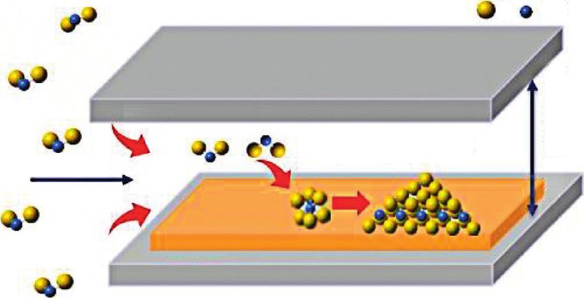
Advances in Materials Science and Engineering 5

 Ar flow PbI2 powder Sandwiched quartz Mica

 Figure 1: Schematic diagram of PbI2 nanosheets prepared by vapor deposition method (https://image.baidu.com/).

information and the sample position. First glue the con- It can be seen from Figure 2 that the morphology control
ductive glue on the sample stage, then put an appropriate of the PbI2 nanosheets, the growth mechanism of PbI2, the
amount of sample on the conductive glue, use the blowing characterization of the composition, and the data obtained
rubber ball to blow gently to blow off the excess sample, and from the optical properties have a very good effect on this
make the sample evenly distributed on the conductive glue; experiment (α > 0.8); the influence of the data obtained from
finally, the sample stage is put into the gold spraying various indicators of the optical performance of MAPbI3
equipment, and the sample is sprayed gold and then taken nanosheets on this experiment is acceptable (α > 0.7). This
out, to be tested. shows that the indicators are reasonable when studying the
 (3) Analysis of the Morphology of the Transmission composition and photoelectric properties of the five selected
Electron Microscope. The electrons transmitted out of the chiral perovskite nanomaterials in this paper. It provides the
sample are magnified and projected on the phosphor screen basis for subsequent experiments.
for observing the graph by the three-stage magnetic lens of
the objective lens, the intermediate mirror, and the pro-
jection lens. Therefore, the image corresponding to the 4.2. Evaluation Index System Based on Inspection Data.
morphology, organization, and structure of the sample is (1) PbI2 Nanosheet Morphology Control. Keeping the growth
displayed on the fluorescent screen. temperature and substrate unchanged, the size of the con-
 finement space and the distance between the substrate and
 the furnace center are important factors affecting the growth
3.4. Establishment of the Model Evaluation Index System.
 of PbI2 nanosheets. Therefore, the size of the confinement
The evaluation index is a specific evaluation item that is
 space (the height between the sandwich quartz plates) is
determined according to the evaluation purpose and can
 compared here. The results of the experiment are shown in
reflect the basic characteristics of the evaluation target.
 Figure 3.
Indicators are specific and measurable and are the obser-
 Figure 3 shows the synthesized PbI2 nanosheets syn-
vation points of your target. Clear conclusions can be drawn
 thesized under different confinement space heights. The
from the actual observation of the object. Typically, the
 confinement space heights are 1 mm, 2 mm, and 3 mm,
metrics system includes three levels of metrics. This is the
 respectively. The crystal size and nucleation density of these
relationship between progressive decomposition and im-
 samples were counted, and the results are shown in Table 2.
provement. Among these, the first-stage evaluation index
 It can be seen from Figure 4 that as the height of the
and the second-stage evaluation index are relatively abstract
 confined space increases from 1 mm to 3 mm, the average
and cannot be used as direct evaluation criteria. The three-
 crystal size increases from 4 μm to 8 μm. But when the height
level assessment indicator should be specific, measurable,
 of the confined space is 3 mm, the synthesized PbI2 nano-
and action-oriented and can be used as a direct basis for
 sheets are no longer uniformly distributed: many small
assessment.
 particles and linear structures appear on the substrate. This is
 similar to the sample obtained without the confined space,
3.5. Statistical Processing. Statistical analysis was performed indicating that as the height of the confined space increases,
with SPSS 13.0 statistical software, the significance test of the the confinement effect decreases. However, PbI2 nanosheets
difference was performed by one-way analysis of variance, with uniform shape and crystal size distribution can be
the difference between the two groups was tested by LSD-t, obtained at both 1 mm and 2 mm limit heights. The nu-
and the photoelectric properties of perovskite nanomaterials cleation density gradually increases as the height of the
were performed by group t-test. P < 0.05 is considered to be confinement space increases, from 36.14 ∗ 104 cm2 at 1 mm
statistically significant. to 125.48 ∗ 104 cm2 at 3 mm, indicating that the size of the
 confinement space is positively correlated with the nucle-
4. Construction and Photoelectric Properties of ation density. When the height of the confinement space
 Perovskite Nanomaterials increases to 3 mm, the uniformity of the PbI2 nanosheets is
 reduced, and the confinement effect is weakened. Therefore,
4.1. Evaluation Index System Based on Index Reliability the effect is best when the height of the confined space is
Testing. Here we perform reliability analysis on all reliability 2 mm, and a uniform and relatively large PbI2 triangular
indicators of each object. The reliability indicators we choose nanosheet can be obtained.
for each object are slightly different. The results are shown in (2) PbI2 Growth Mechanism. It can be seen from Figure 5
Table 1. that for the case of no confined space, PbI2 has both
6 Advances in Materials Science and Engineering

 Table 1: Data sheet of evaluation index system for index reliability testing.
 Very clear Clear General Not clear Chaotic Alpha
PbI2 nanosheet morphology control 3.98 3.81 4.51 0.79 0.47 0.7281
PbI2 growth mechanism 3.55 3.65 4.45 0.47 0.54 0.7349
Component structure characterization 3.87 3.86 4.76 0.66 0.49 0.7425
Optical properties 3.58 4.14 4.70 0.52 0.41 0.7762
Optical properties of MAPbI3 nanosheets 3.62 3.98 4.52 0.53 0.42 0.8294

 Indicator Relisbility Test Analysis Chart
 5 4.45
 4.51 4.76
 4.5 4.7 4.52
 4 3.98 3.87 3.98
 3.65 4.14
 3.5 3.81 3.86 3.62
 3.55 3.58
 3
 Value

 2.5
 2
 1.5
 0.79
 1 0.47 0.66 0.52 0.53
 0.5 0.47 0.54 0.42
 0.49 0.41
 0
 PNMC PGM CSC OP OPMN
 Attributes

 Very Clear Not Clear
 Clear Chaotic
 General
 Figure 2: Indicator reliability test analysis chart.

 (a) (b) (c)

Figure 3: Influence of the height of the confined space on the morphology of PbI2 nanosheets (https://image.baidu.com/). (a) PbI2
nanosheets under the restricted space height of 1 mm. (b) PbI2 nanosheets under the restricted space height of 2 mm. (c) PbI2 nanosheets
under the restricted space height of 3 mm.

 Table 2: Data sheet of evaluation index system for index reliability testing.
Restricted space height Average crystal size (μm) Nuclear density (∗ 104 cm2 )
1 mm 4 36.14
2 mm 6 67.78
3 mm 8 125.48

triangular and hexagonal morphologies, indicating that the process, so that the gas source concentration is evenly
growth process has dynamic instability, and the concen- distributed on the substrate. In the nucleation stage, the low
tration and flow rate of the gaseous source of PbI2 are source concentration in the confined space effectively re-
constantly changing. This greatly limits the controllable duces the nucleation density; in the epitaxial growth stage, it
growth of PbI2, thus limiting their further applications. can provide a stable source supply and realize the uniform
When the sandwich quartz plate is introduced as the con- growth of PbI2 nanosheets. As the substrate distance in-
fined space, it cannot only ensure that the PbI2 gaseous creases, the PbI2 concentration gradually decreases, resulting
source can be successfully transferred to the substrate, but in thinner nanosheets. The confined space reduces nucle-
also produce a stable gaseous source concentration delivery ation density and provides a relatively stable gas source
Advances in Materials Science and Engineering 7

 12 150 Table 3: Component structure characterization data sheet.
 11
 10 130 Degree (001) (002) (003) (004)
 125.48

 Nucleation Density
 9 10 1.29 2.59 2.31 2.75
 110
 Crystal Size

 8 8 20 2.68 2.70 2.80 3.39
 7 90 30 3.43 3.97 3.47 4.20
 6 6 40 3.45 4.24 3.76 4.78
 5 67.78 70 50 4.46 4.44 4.96 5.38
 4 4 50 60 4.32 5.02 4.94 5.51
 3
 36.14
 2 30
 1mm 2mm 3mm
 Space Height 7

 Average Crystal Size (μm) 6 5.38 5.51
 4.96 5.02
 4.78
 Nuclear Density (∗105cm2) 5
 4.24
 4.46 4.32
 4.94
 4.2
 3.97 4.44
 4 3.45 3.76

 Value
Figure 4: Relationship between crystal size and nucleation density 3.39 3.43 3.47
 2.59 2.75 2.8
and confinement space height. 3 2.31
 2.7
 2.68
 2 1.29

 I Pb 1
 0
 10 20 30 40 50 60
 Confined space

 Degree
 Quartz
 [001] [003]
 Epitaxy growth
 Limited [002] [004]
 transport Figure 6: Component structure characterization analysis diagram.
 Mica
 with the X-ray diffraction pattern results. These all indicate
 that the obtained PbI2 nanosheets are single crystals with
Figure 5: Schematic diagram of the growth mechanism of PbI2
 high quality and uniformity.
nanosheets in a confined space (https://image.baidu.com/).
 (4) Optical Property Analysis. The optical properties of
 PbI2 nanosheets were studied, and the Raman peak positions
supply environment, which can overcome dynamic insta- of samples with different thicknesses were studied. The
bility during PbI2 growth and achieve uniform and con- results are shown in Table 4.
trollable preparation for the shape and thickness of PbI2 It can be seen from Figure 8 that the Raman peak of the
nanosheets. mica substrate is relatively weak, and its influence on the test
 (3) Characterization of Composition Structure. Through results can be ruled out. All samples have characteristic
X-ray diffraction pattern, X-ray photoelectron spectroscopy, peaks at 75, 100, and 125, which are attributed to the three
the phase structure, and chemical state of PbI2 nanosheets vibration mode peaks of Eg , A1g , and A2u in PbI2, respec-
were studied. The X-ray diffraction pattern was used to tively. As the thickness of PbI2 increases, the peak intensity
determine the crystal phase structure of the sample, and the of all peaks becomes stronger and the half-width becomes
results are shown in Table 3. narrower, but the position of the characteristic peak remains
 It can be seen from Figure 6 that all the peak positions in unchanged.
the figure are in good agreement with the hexagonal phase (5) Study on Gas Phase Transformation and Optical
PbI2, and only the (001) plane diffraction peak appears, Properties of MAPbI3 Nanosheets. Through precise control of
which indicates that the out-of-plane growth direction of reaction conditions and related characterization, we have
PbI2 nanosheets is the [001] direction. obtained high-quality PbI2 nanosheets with uniform mor-
 We conducted transmission electron microscopy anal- phology and controllable size, which provides an important
ysis of the PbI2 crystal structure, and the transmission basis for the two-step preparation of MAPbI3 nanosheets.
electron microscopy sample was obtained by sample The obtained MAPbI3 nanosheets were characterized by
transfer. The result is shown in Figure 7. related optical properties, and the results are shown in
 The high-resolution electron microscope image of the Table 5.
PbI2 nanosheet is shown in Figure 7(a). The distance be- It can be seen from Figure 9 that the peak position of the
tween the crystal planes is 0.228 nm, which corresponds to fluorescence spectrum obtained by Gaussian fitting is
the (110) plane of PbI2. The selected area electron diffraction 800 nm, and the half-value width is about 45 nm. The half-
pattern in Figure 7(b) also proves that the high-resolution value width can reflect the crystalline properties of the
exposed crystal plane is the PbI2 (110) crystal plane, and the material, and the smaller the value, the better, which fully
direction perpendicular to the crystal plane is the [001] indicates that the obtained nanosheets have high crystallinity
crystal orientation. The results obtained are also consistent and at the same time indicates that the converted perovskite
8 Advances in Materials Science and Engineering

 PbI2 high resolution PbI2 high-resolution corresponding selected
 transmission spectrum area electron diffraction pattern
 (a) (b)

 Figure 7: Transmission electron microscope analysis chart (https://image.baidu.com/).

 Table 4: Optical properties data sheet.
Raman shift Mica 5 nm 10 nm 30 nm 40 nm 80 nm 100 nm
50 2.58 2.46 2.98 2.34 2.98 2.36 2.58
75 2.73 3.17 3.53 2.73 2.83 3.43 3.04
100 2.57 2.97 2.77 2.76 2.68 2.45 2.95
125 3.95 3.21 3.5 3.85 3.58 3.51 3.79
150 2.79 2.71 2.86 3.07 3.42 3.06 2.96
175 2.66 2.84 2.78 2.63 2.66 2.87 2.97

 4
 3.95
 3.8 3.85
 3.6 3.53 3.79
 3.58 3.42
 3.4 3.43 3.51
 3.17 3.5
 3.2 3.07
 Value

 2.98 3.04 2.97 2.97
 3 3.21 3.06 2.87
 2.98 2.95 2.77 2.96 2.84
 2.83 2.86
 2.8 2.58 2.73 2.76 2.79 2.78
 2.68 2.66
 2.6 2.58 2.57 2.66
 2.46 2.73 2.71
 2.4 2.45 2.63
 2.36
 2.2 2.34
 2
 50 75 100 125 150 175
 Raman Shift

 mica 40 nm
 5 nm 80 nm
 10 nm 100 nm
 30 nm
 Figure 8: Optical property analysis chart.

 Table 5: MAPbI3 nanosheet optical performance data sheet.
Wavelength MAPbI3 PbI2 Mica
550 0.1 0.3 0.5
600 0.1 0.3 0.5
650 0.1 0.3 0.5
700 0.1 0.3 0.5
750 0.4 0.6 0.8
800 1.0 1.4 2.0
850 0.4 0.6 0.8
900 0.1 0.3 0.5
950 0.1 0.3 0.5
Advances in Materials Science and Engineering 9

 2.5 introduces a limited space to suppress the dynamic insta-
 bility during the PbI2 vapor deposition process, so as to
 2 obtain high-quality PbI2 nanosheets with uniform and
 controllable morphology and thickness. At the same time,
 1.5 PbI2 can be converted into MAPbI3 nanosheets by chemical
Value

 vapor deposition, which provides a method for the uniform
 1 and controllable synthesis of two-dimensional perovskite
 and also provides a basis for its performance research. The
 0.5 current field of chiral perovskites is a brand-new research
 field, which is both an opportunity and a challenge. A lot of
 0
 basic and applied work needs to be carried out.
 550 600 650 700 750 800 850 900 950 This paper improves the perovskite vapor phase syn-
 Wavelength thesis method, reduces the cost of preparing the vapor phase
 method, and obtains a uniform and controllable perovskite
 MAPbI3 nanomaterial. Although we have achieved some results from
 PbI2 the preparation of the material, there are still aspects that
 mica require further development. Although uniform and con-
Figure 9: MAPbI3 nanosheet optical performance analysis trollable PbI2 and MAPbI3 nanosheets were obtained with a
diagram. limited space method, in-depth studies on that method and
 the material obtained are lacking. Movement instability
 during growth of nanomaterials is universal. This experi-
nanosheets have good uniformity. MAPbI3 exhibits strong ment improves the preparation of PbI2 nanosheets and
light absorption characteristics when the wavelength is less overcomes this phenomenon. However, the same problems
than 800 nm, which also proves that MAPbI3 not only has that exist in the fabrication of other nanomaterials have not
good fluorescence spectrum luminescence properties, but been explored in depth.
also has strong light absorption characteristics.
 Data Availability
5. Conclusions
 No data were used to support this study.
The gas phase method is an important method for preparing
high-quality perovskite nanomaterials. Improving the Conflicts of Interest
controllability of the gas phase method and reducing the
production cost are of great significance for further per- The author declares that there are no conflicts of interest
formance research and commercial application of the pe- regarding the publication of this article.
rovskite. This paper takes organic perovskite MAPbI3
nanosheets as the research object, through the improvement References
of the gas phase method and the introduction of limited
space to improve the controllability of the preparation of [1] S. T. Ha, R. Su, J. Xing, Q. Zhang, and Q. Xiong, “Metal halide
precursor PbI2 nanosheets, then obtain uniform MAPbI3 perovskite nanomaterials: synthesis and applications,”
nanosheets, and further explore its growth mechanism and Chemical Science, vol. 8, no. 4, pp. 2522–2536, 2017.
study its photoelectric performance. By introducing a lim- [2] B. Halford, “Nanomaterials Chiral gold nanoparticles,”
ited space, the PbI2 nanosheets with uniform and control- Chemical and Engineering News: \”news Edition\” of the
 American Chemical Society, vol. 96, no. 17, pp. 10-11, 2018.
lable morphology, size, and thickness were successfully
 [3] M. M. Riba, C. G. Oliveras, D. B. Amabilino, and
prepared by physical vapor deposition. The confined space is A. C. González, “Supramolecular block copolymers incor-
the key to realize the uniform growth of PbI2 nanosheets. It porating chiral and achiral chromophores for the bottom-up
provides a relatively stable growth environment and avoids assembly of nanomaterials,” Journal of Porphyrins & Phtha-
the dynamic instability during the growth of PbI2. This locyanines, vol. 23, no. 07n08, pp. 916–929, 2019.
confined space vapor deposition method can improve the [4] X. Shang, I. Song, H. Ohtsu et al., “Supramolecular nano-
uniformity and controllability of the preparation of PbI2 and structures of chiral perylene diimides with amplified chirality
MAPbI3 nanosheets, which provides a basis for further for high-performance chiroptical sensing,” Advanced Mate-
research of MAPbI3 nanomaterials and also has reference rials, vol. 29, no. 21, pp. 1605828.1–1605828.7, 2017.
significance for the controllable growth of other [5] B. Han, L. Shi, X. Gao et al., “Ultra-stable silica-coated chiral
nanomaterials. Au-nanorod assemblies: core–shell nanostructures with en-
 hanced chiroptical properties,” Nano Research, vol. 9, no. 2,
 The introduction of chirality into the optical commu-
 pp. 451–457, 2016.
nication system can not only increase another new di- [6] H. Kong, X. Sun, L. Yang, X. Liu, H. Yang, and R. H. Jin,
mension of high-speed optical information transmission, “Chirality detection by Raman spectroscopy: the case of
but also significantly increase the information capacity. enantioselective interactions between amino acids and
Therefore, chiral perovskite nanomaterials provide broad polymer-modified chiral silica,” Analytical Chemistry, vol. 92,
application prospects in this regard. This paper mainly no. 21, pp. 14292–14296, 2020.
10 Advances in Materials Science and Engineering

 [7] S. Wang, J. Yu, J. Li, and Y. Lin, “Prevalence and imaging [22] Y. S. Shmaliy, S. H. Khan, S. Zhao, and O. M. Ibarra, “General
 features of superior canal dehiscence based on HRCT,” unbiased FIR filter with applications to GPS-based steering of
 Chinese Journal of Medical Imaging Technology, vol. 34, no. 10, oscillator frequency,” IEEE Transactions on Control Systems
 pp. 1465–1468, 2018. Technology, vol. 25, no. 3, pp. 1141–1148, 2017.
 [8] V. Y. Gus’kov and V. N. Maistrenko, “New chiral stationary [23] N. Rozzani, I. S. Mohamed, and S. A. N. S. Yusuf, “Technology
 phases: preparation, properties, and applications in gas for Islamic microfinance’s disbursement and repayment
 chromatography,” Journal of Analytical Chemistry, vol. 73, system,” International Journal of Social Economics, vol. 43,
 no. 10, pp. 937–945, 2018. no. 12, pp. 1271–1283, 2016.
 [9] X. Wang, B. Liu, Y. Yu et al., “Application value of chest [24] A. Abburi, M. Ali, and P. V. Moriya, “Synthesis of meso-
 multi-detector spiral CT in diagnosis and follow-up of corona porous silica nanoparticles from waste hexafluorosilicic acid
 virus disease 2019,” Chinese Journal of Medical Imaging of fertilizer industry,” Journal of Materials Research and
 Technology, vol. 36, no. 3, pp. 400–404, 2020. Technology, vol. 9, no. 4, pp. 8074–8080, 2020.
[10] M. C. Weidman, A. J. Goodman, and W. A. Tisdale, “Colloidal [25] K. Reals, “Industry urges improved access to aircraft cabins
 halide perovskite nanoplatelets: an exciting new class of for the disabled,” Aviation Week & Space Technology, vol. 180,
 semiconductor nanomaterials,” Chemistry of Materials: A no. 13, pp. 70-71, 2018.
 Publication of the American Chemistry Society, vol. 29, no. 12,
 pp. 5019–5030, 2017.
[11] M. Jiang, W. Guo, T. Jiao, and Q. Xu, “Metal ion substitution
 effect and component regulation of perovskite-type La1–x Cax
 CrO3 nanomaterials,” Science of Advanced Materials, vol. 9,
 no. 7, pp. 1231–1235, 2017.
[12] N. A. Gibson, B. A. Koscher, A. P. Alivisatos, and S. R. Leone,
 “Excitation intensity dependence of photoluminescence
 blinking in CsPbBr3 perovskite nanocrystals,” The Journal of
 Physical Chemistry, C. Nanomaterials and Interfaces, vol. 122,
 no. 22, pp. 12106–12113, 2018.
[13] A. S. Alsubaie, “Recent advances in bismuth ferrite nano-
 materials: synthesis, characterization and application,” Jour-
 nal of Chemical, Biological and Physical Sciences, vol. 11, no. 2,
 pp. 101–111, 2021.
[14] M. Yamauchi, Y. Fujiwara, and S. Masuo, “Slow anion-ex-
 change reaction of cesium lead halide perovskite nanocrystals
 in supramolecular gel networks,” ACS Omega, vol. 5, no. 24,
 pp. 14370–14375, 2020.
[15] H. Wang, Y. Liang, L. Liu, J. Hu, P. Wu, and W. Cui,
 “Enriched photoelectrocatalytic degradation and photoelec-
 tric performance of BiOI photoelectrode by coupling rGO,”
 Applied Catalysis B Environmental, vol. 208, pp. 22–34, 2017.
[16] B. Hu, Y. Wang, C. Hu, and X. F. Zhou, “Design, fabrication
 and high efficient visible-light assisted photoelectric-syner-
 gistic performance of 3-D mesoporous DSA electrodes,”
 Materials and Design, vol. 91, pp. 201–210, 2016.
[17] Y. Jun, Y. Li, Z. Jia, and Z. Dong, “Enhanced photoelectric
 performance of composite nanostructures combining
 monolayer graphene and a RbAg4I5 film,” Applied Physics
 Letters, vol. 110, no. 21, pp. 1–4, 2017.
[18] W. Luan, C. Zhang, L. Luo, B. Yuan, L. Jin, and Y. S. Kim,
 “Enhancement of the photoelectric performance in inverted
 bulk heterojunction solid solar cell with inorganic nano-
 crystals,” Applied Energy, vol. 185, no. 2, pp. 2217–2223, 2016.
[19] H. Li and W. Gao, “Detection sensitivity calculation model
 and photoelectric detection performance analysis on laser
 light screens,” IEEE Sensors Journal, vol. 16, no. 11,
 pp. 4258–4264, 2016.
[20] Y. Deng, Z. Ma, F. Ren, and G. Wang, “Improved photo-
 electric performance of DSSCs based on TiO2 nanorod array/
 Ni-doped TiO2 compact layer composites film,” Journal of
 Solid State Electrochemistry, vol. 23, no. 11, pp. 3031–3041,
 2019.
[21] F. Li, G. Chen, and X. Fu, “Erratum to: comparison of effect of
 gear juicer and colloid mill on microstructure, polyphenols
 profile, and bioactivities of mulberry (morus indica L.),” Food
 and Bioprocess Technology, vol. 9, no. 7, pp. 1246–1248, 2016.
You can also read