Low Power Square Root Carry Select Adder Using AVLS-TSPC-Based D Flip-Flop
←
→
Page content transcription
If your browser does not render page correctly, please read the page content below
ORIGINAL ARTICLE
                                                                                                                            Electrica 2021; XX(XX): 1-11

Low Power Square Root Carry Select Adder Using
AVLS-TSPC-Based D Flip-Flop
Premananda Belegahalli Siddaiah , Nikhil Kiran Jayanthi , Samana Hanumanth Managoli
Department of Electronics & Telecommunication Engineering, RV College of Engineering, Bengaluru, Karnataka, India

Cite this article as: B. S. Premananda, K. J. Nikhil and S. H. Managoli. “Low Power Square Root Carry Select Adder using AVLS-TSPC-based D Flip-flop,”
Electrica, DOI: 10.5152/electr.2021.21024.

ABSTRACT

Speed, power, and area are the parameters to be considered while designing any integrated circuits including adder circuits. Low-power computation
circuits play an important role in the very large-scale integration (VLSI) industry. Carry select adder (CSLA) is one of the fastest adders available and used to
combat carry rippling. The square root of carry select adder (SCSLA) is a special case of CSLA. Since the SCSLA functions at high speed, it becomes vital to
minimize the power dissipation and optimize the entire adder circuit. Adaptive voltage level at source (AVLS) is a technique used to minimize the power
utilization of the circuit by decreasing the supply voltage. True-single phase clocking (TSPC) is used to design D flip-flop which reduces both the area and
power. The proposed 16-bit adder architectures, one with AVLS normal TSPC-based D flip-flop and the other with AVLS modified TSPC D flip-flop has power
reduction of 53.91% and 58.12% respectively, when compared with existing architectures in complementary metal-oxide-semiconductor (CMOS) 180 nm
technology. Also, the proposed architectures, when implemented in CMOS 45 nm technology showed a power reduction of 82.75% and 82.93% respectively.
The circuits are realized using Cadence Virtuoso and simulated using Cadence Spectre. Both the adders are power-efficient and operate at high speed.
Index Terms—Adaptive voltage level at source (AVLS), carry select adder (CSLA), D flip-flop, low power, square root of carry select adder (SCLSA).

                                            I. INTRODUCTION

                                            Logic style and micro-architecture are the critical design features for any arithmetic circuit [1].
                                            Arithmetic circuits are used to execute various calculation purposes such as addition, subtrac-
                                            tion, multiplication, address calculation, media access control address (MAC) unit, etc. [2]. Low-
                                            power computation circuits play an important role in the VLSI industry. In processors, such as
                                            the digital signal processor, the essential modules are the adders. The MAC unit utilizes a full
                                            adder, which significantly affects the efficiency of the complete system. Multiplication is also
                                            an imperative arithmetic operation which is implemented using addition of partial products
                                            [3]. Hence, low-power adder becomes the need of the hour for achieving high-performing
                                            processors and systems.
Corresponding Author:
Premananda Belegahalli Siddaiah
                                            The addition in the adders is limited by the propagation of the carry signal. Carry select adder
E-mail:                                     (CSLA) is better than ripple carry adder (RCA) as it has less delay. Considering the carry propa-
premanandabs@gmail.com
                                            gation design for adders, an acceptable compromise can be achieved between cost and per-
Received: March 8, 2021                     formance while using the carry select method [4]. Linear CSLA uses two rows of RCAs, one
Accepted: August 4, 2021                    operating with carry_in = “0” and the other with carry_in = “1.” As a result, two predetermined
Available Online Date: September            sets of sum and carry_out signals are obtained. The precise output is selected using the original
9, 2021                                     carry_in. The square root carry select adder (SCLSA) is a variant of CSLA. The SCSLA design is an
DOI: 10.5152/electr.2021.21024              advancement over the standard (linear) CSLA in terms of power dissipated and operating speed
                                            [5]. Carry is propagated to successive blocks through multiplexers. Due to the inclusion of addi-
                                            tional RCAs in SCSLA, it consumes more power as compared to RCA. Hence, it becomes neces-
                                            sary to reduce the power consumption of SCSLA to implement it in low-power applications.
Content of this journal is licensed
under a Creative Commons                    The SCSLA can be made low power using true single-phase clock (TSPC)-based D flip-flops
Attribution-NonCommercial 4.0
                                            in place of RCAs. The TSPC-based D flip-flop is a dynamic CMOS-based flip-flop that aims at
International License.

                                                                               1
Electrica 2021; XX(XX): 1-11
                                      Premananda et al. Low Power Square Root Carry Select Adder

operating at an elevated speed. However, in an effort to fur-              level at source was perceived to utilize lesser power when con-
ther lower the consumption of power by SCSLA, the adaptive                 trasted with that of adaptive voltage level at ground (AVLG).
voltage level at source (AVLS) approach has been incorporated.             Therefore, it was then integrated with TSPC-based flip-flop. The
Adaptive voltage level at source is a technique in which the               TSPC circuit was designed using 10T. This methodology, with-
power consumption is reduced by lowering the supply poten-                 out AVLS technology, was found to utilize 21.9 μW of power
tial [6]. A sleep-control signal, often the clock signal, is used to       but with AVLS unification, it was then decreased to 9.304 μW
regulate the operation of the AVLS circuit’s transistors. It lowers        providing an insignificant expansion in the area.
the voltage across the gate source and drain, hence, lowering
the leakage power. The AVLS circuit’s output serves as the sup-            There is a need for a faster arithmetic processing unit due
ply voltage for the SCSLA.                                                 to rapid growth in the technology used these days, there-
                                                                           fore, CSLA was considered. Linear CSLA was implemented in
This study emphasizes on proposing a 16-bit SCSLA architec-                Naik and Rao [7] by replacing RCA with BEC. The authors also
tures that dissipates low power with less carry rippling delay.            implemented a new approach of using D-latch so as to further
The proposed SCSLA uses AVLS logic with TSPC-based D flip-                 reduce the power utilization. Results depicted the reduction
flops instead of RCAs. By incorporating AVLS and TSPC-based                of delay of CSLA architecture than the current models of BEC-
techniques in the proposed adder, the power and speed                      based CSLA architecture and RCA-based architectures.
parameters are optimized respectively. Cadence Virtuoso is uti-
lized to realize the proposed architecture, while the simulation           With efficient usage of area and reducing the power dissipa-
is carried out on Cadence Spectre.                                         tion of the adder, the comprehensive performance of the pro-
                                                                           cessors can be enhanced. In the authors suggested the notion
The paper is categorized into various sections. Frameworks,                of using TSPC-based D-FF instead of using RCA and BEC in the
techniques, and realizations are reviewed in section II. Section           conventional method. This prototype of 16-bit CSLA with nor-
III elucidates the CSLA and the AVLS technique. The implemen-              mal TSPC-based D-FF used a fewer number of transistors as
tation of the TSPC-based circuits and proposed architecture is             compared to RCA. Therefore, the power consumed was less
explained in section IV. Section V analyses the simulation results         compared to other circuits. The utilization of D-FF that trig-
and compares the proposed adders to the existing adder, with               gers at the positive edge of the clock along with modified
regard to power utilized and delay parameters. Section VI con-             TSPC resulted in lesser power consumption and the product of
cludes the work and puts forth the future scope to it.                     power-delay was reduced [8].

II. ASSOCIATED WORKS                                                       Ponnusamy and Palaniappan [9] dealt with a new approach of
                                                                           implementing a negative edge-triggered D-FF instead of the
The arithmetic, as well as logic units in microprocessors and              regular D-FF with the 16-bit CSLA. This continuous switching
microcontrollers, consists of a full adder which acts as the basic         of inputs directly impacted the outputs of the adder on the
arithmetic circuit. Hence, the overall capability of circuits that         application of the enable signal. Their methodology was imple-
consist of the full adder can be upgraded by improving the                 mented in a partitioned Dadda multiplier using the microwind
performance of the adder. Nigam and Singh [2] described a                  tool that worked at a faster pace. Results were marked with
relative analysis of full adders consisting of 28T and 14T. The            the length and width trade-off for power. The suggested CSLA
evaluation was done owing to the consumption of power, by                  architecture resulted in power consumption of 0.296 mW.
altering the values of different parameters. It was remarked and
proved that the 14T full adder consumes less power as com-                 A new methodology known as TSPC flip-flop was used to
pared to the 28T full adder. The implementation and simulation             compensate for the generation of leakage current at dynamic
were done with Empyrean Aether employing 45 nm technol-                    nodes of the transistor. Lee and Jang [10] proposed this tech-
ogy libraries.                                                             nique for covering a vast range of operational frequencies in
                                                                           the CMOS processes. A gated inverter (GI) was used to build
The structure of the CSLA was modified to overcome power                   three feedback circuits which were then used to implement
dissipation problems [4]. A TSPC-based D-FF was used to                    the suggested method of TSPC-based flip-flop. The suggested
replace the carry input block. The suggested configuration was             design was provided with a 1 V power supply and is operated at
better with regard to power as well as area when compared to               2 GHz frequency. The results concluded that the recommended
the standard and CSLA based on binary to excess-1 converter                TSPC-based flip-flop shows zero error at low frequencies of
(BEC), with a power consumption of 7.951 mW for 16 bits.                   1 MHz.

Anirvinnan et al., [6] suggested a new technique for low-power             The surveys of various models of D flip-flop depend on the
application, by using D flip-flops with minimal power consump-             TSPC rationale which permits to address the plan of D-FF with
tion. The realization of latches and flip-flops was achieved by            a more modest region and lower power utilization when con-
this strategy of the TSPC circuit which lessened the skew issues           trasted with the master–slave arrangement-based D flip-flop
in the clock. By adapting AVLS into the circuits based on TSPC,            [11]. The paper examined the execution of various TSPC-based
the target of low-power was also achieved. Adaptive voltage                D flip-flops and their correlation regarding power, delay, and

                                                                       2
Electrica 2021; XX(XX): 1-11
                                      Premananda et al. Low Power Square Root Carry Select Adder

transistors. In contrary with other flip-flops, it was seen that the       speed is a significant parameter in numerous applications,
5T TSPC-based D-FF is better in execution with less utilization            CSLA is preferred to overcome the delay of RCA:
of power from the comparison result and analysis.
                                                                           S  A  B  Carryin                                            (1)
The optimization of power plays a crucial role in low-voltage
and low-power applications. Gupta and Saxena [12] presented                Cout  A  B  B  Carryin  Carryin  A                       (2)
an architecture of a D-FF circuit utilizing AVL methods for low-
power activity. The realization of this D-FF was done by making            B. Carry Select Adder With Ripple Carry Adder
use of H-Spice with 130 nm technology. Results of simulation               The linear n-bit CSLA is divided into m-blocks with equal bit-
showed a reduction of power for the suggested cell adapt-                  size. But there is a mismatched delay while obtaining the
ing the AVL procedure. Elimination of unnecessary switching                carry and sum signals. In SCSLA, the n-bit adder is divided into
of the transistors, with respect to the clock signal in memory             m-blocks with unequal bit-size. For a 16-bit adder, it is divided
elements, found that the power dissipation can be reduced                  into five blocks with sizes of 2, 2, 3, 4, and 5-bits respectively
to a larger extent than the current methodology. The AVLS                  from the rightmost block. Except for the rightmost block, all
technique had a power consumption of 1.13 nW, whereas the                  other blocks consist of two RCAs with each having carry_in
AVLG technique had a power consumption of 2.25 nW. Carry                   “0” and “1,”respectively. The multiplexer (MUX) helps to over-
select adder proposed in [3] dissipates less power but occupies            come the mismatched delay present in linear CSLA [14]. The
more area as adiabatic logic is incorporated in the design of the          SCSLAperforms its operation very fast as compared to RCA
adder. There is a need to design a SCLSA which reduces power,              because it does not wait for carry from the preceding block,
delay, and area.                                                           rather performs the addition with the independent given carry
                                                                           signal. Hence, the sum and carry outputs are obtained at the
III. DESIGN THEORY OF ADDERS                                               MUX output. Fig. 1 shows a 16-bit SCSLA with RCA [4].

Adders play a significant role as the basic arithmetic circuit in          C. The Square Root Carry Select Adder With True-Single
signal processors, microprocessors, and other applications.                Phase Clocking-Based D Flip-Flop
Hence, improving the performance of the adders portrays an                 The 16-bit SCSLA using the normal positive edge-triggered
imperative part in upgrading the overall circuit.                          D-FF uses the RCA with the clock as carry_in for addition. When
                                                                           the clock becomes zero, the RCA performs the addition with
A. Ripple Carry Adder                                                      carry_in = “0,” and sends the result to the D-FF. During the posi-
The RCA is developed by cascading one-bit full adders to gen-              tive edge of the clock, this result is accumulated in the D-FF.
erate the sum as well as the carry signals. The sum and carry              When the clock becomes high (or logic “1”), the RCA performs
signals of the one-bit full adders are generated according to              the addition with carry_in = “1,” and sends it directly to the
(1) and (2). The subsequent block produces a sum only after                multiplexer, as the D-FF acts as a latch when the clock becomes
the preceding block is summed. The carry from the precedent                high. The actual sum and carry are produced at the end of
blocks is passed onto the succeeding blocks for addition [13].             one complete clock cycle. An altered TSPC-based D-FF can be
This configuration is efficient in terms of area, but the delay            designed to decrease the utilization of power by removing one
in propagation of carry signal from the previous blocks to the             transistor from the normal TSPC-based D-FF and by making the
next results in the adder functioning at a slower speed. Since             required changes.

 Fig. 1. Sixteen-bit square root carry select adder (SCSLA)with ripple carry adder (RCA).

                                                                       3
Electrica 2021; XX(XX): 1-11
                                       Premananda et al. Low Power Square Root Carry Select Adder

                                                                          The normal TSPC-based D flip-flop is implemented using
                                                                          11 transistors. Only a single clock is seen in TSPC which is
                                                                          never inverted. The clock signal is given to both NMOS and
                                                                          PMOS transistors. The output is continuously affected by the
                                                                          switching of inputs with variation in the clock. A TSPC clock
                                                                          minimizes the overall power consumption of the circuit as it
                                                                          requires fewer transistors, and thereby increases the speed of
                                                                          the circuit. True-single phase clocking acts as master and slave
                                                                          circuits.

                                                                          The SCSLA can be made power and speed efficient by
                                                                          implementing D-FF rather than the RCA in the second row.
                                                                          Fig. 3 displays the realization of a normal TSPC-based D flip-flop
                                                                          (11 T). The remodeled TSPC-based D-FF can be implemented
                                                                          by removing one transistor from the normal TSPC-based D flip-
                                                                          flop [4]. As the remodeled TSPC-based D-FF can be realized
                                                                          using 10 transistors, it dissipates less power in contrast with
                                                                          the normal TSPC-based D-FF. Fig. 4 shows the implementation
                                                                          of the modified TSPC-based D-FF.

                                                                          Table I lists the power and delay values of the full adders. The
                                                                          TSPC-based D flip-flop consumes less power compared to the
                                                                          one-bit full adder. Hence, the normal and modified TSPC-based
                                                                          D flip-flop is preferred over RCA in SCSLA. Keeping in mind the
 Fig. 2. Principle adaptive voltage level at source (AVLS) circuit.
                                                                          goal to further decrease the power utilization of the normal
                                                                          and modified TSPC-based D flip-flop, the AVLS technique can
D. Adaptive Voltage Level                                                 be implemented. Since the D-FF is a sequential segment and
To achieve minimal dissipation of power by the circuit and to             makes use of a clock signal for its functioning, the same can be
make it operate at low power, a technique called adaptive volt-           used as the control signal for the AVLS circuit. Fig. 5 shows the
age level (AVL) is used. The AVL circuit is controlled by a sleep-        realization of AVLS normal TSPC-based D-FF.
control signal. The AVLG raises the potential of the ground,
whereas the AVLS lowers the supply voltage potential, accord-             In the AVLS circuit, the NMOS transistors are continuously in
ingly decreasing the dissipation of power by the entire circuit.          the ON state, as they are forward biased. The PMOS transistor
Adaptive voltage level at source consists of a parallel connec-           has the clock signal as the input and hence toggles from one
tion of two NMOS transistors and one PMOS transistor. The                 state to the other. As a result, the minimal discharge current
two NMOS transistors are in turn concatenated in series. The              flows through the PMOS of AVLS, thereby reducing the utiliza-
clock signal is connected to the PMOS transistor node which               tion of power by the circuit. Fig. 6 shows the realization of AVLS
acts as the input to the circuit. On the other hand, the supply is        modified TSPC-based D-FF. Table II displays the power and
given to the input of NMOS transistors. The supplied clock acts           delay results of AVLS normal and modified TSPC-based D flip-
as the sleep signal which controls the functioning of the AVLS            flop when realized using 45 nm technology libraries. It is evi-
circuit. Fig. 2 shows a principal AVLS circuit that is positioned         dent that these architectures consume less power compared
in between the supply voltage and the SCSLA to lessen the                 to the values listed in Table I.
potential of the supply node.
                                                                          Two designs have been proposed as a part of the proposed
IV. DESIGN AND IMPLEMENTATION OF ADDER                                    architecture. The proposed-1 design has AVLS normal TSPC-
ARCHITECTURES                                                             based D flip-flop (Fig. 5) and the proposed-2 design has AVLS
                                                                          modified TSPC-based D flip-flop (Fig. 6). These flip-flops are
Cadence Virtuoso is used to implement all the circuits using              used instead of RCA in the second row of each block in the 16-bit
both 180 nm and 45 nm technologies. Cadence Spectre is used               SCSLA. Fig. 7 shows the proposed-1 and proposed-2 designs
to carry out the simulation of the frameworks. The SCSLA can be           of 16-bit SCSLA with normal/modified TSPC-based D flip-flop.
modified by implementing a D flip-flop instead of the second              The AVLS circuit is placed between the supply voltage and the
RCA in each block, with a motive to decrease the utilization of           16-bit SCSLA adder, with a clock signal as the input to the AVLS
power along with the delay of the SCSLA. The D-FF can be real-            circuit.
ized to work at a faster rate by incorporating TSPC to the D-FF.
True-single phase clocking allows the true phase of the clock             The clock signal is common to both AVLS and 16-bit CSLA
and does not take the complement of it. The SCSLA with TSPC-              circuits. Due to this, the leakage flow of the PMOS transistor
based D-FF is efficient with reference to power, area, and delay.         is reduced, thereby minimizing the dissipation of power by

                                                                      4
Electrica 2021; XX(XX): 1-11
                                      Premananda et al. Low Power Square Root Carry Select Adder

  Fig. 3. Normal true-single phase clocking (TSPC)-based D flip-flop.

  Fig. 4. Modified TSPC-based D flip-flop.

 TABLE I. POWER AND DELAY ANALYSIS OF 1-BIT FULL ADDER, NORMAL, AND MODIFIED TRUE-SINGLE PHASE CLOCKING-BASED
 D FLIP-FLOP IN 45 NM TECHNOLOGY

 Architecture                                                     Transistor Count           Power (μW)    Delay (ps)

 1-bit full adder                                                           28                     10.28     23.82

 Normal TSPC-based D flip-flop                                              11                     1.932     13.77

 Modified TSPC-based D flip-flop                                            10                     1.849     13.96
TSPC, true-single phase clocking.

                                                                        5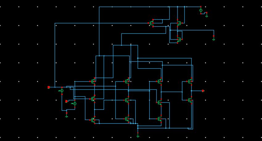
Electrica 2021; XX(XX): 1-11
                                     Premananda et al. Low Power Square Root Carry Select Adder

Fig. 5. Adaptive voltage level at source normal TSPC-based D flip-flop.

Fig. 6. Adaptive voltage level at source modified TSPC D flip-flop.

                                                                      6
Electrica 2021; XX(XX): 1-11
                                                Premananda et al. Low Power Square Root Carry Select Adder

 TABLE II. POWER AND DELAY ANALYSIS OF AVL NORMAL AND MODIFIED TRUE-SINGLE PHASE CLOCKING-BASED D FLIP-FLOP IN
 45 NM TECHNOLOGY

 Architecture                                                               Transistor Count              Power (μW)             Delay (ps)

 AVLS normal TSPC-based D flip-flop                                                 14                        1.614                14.98

 AVLS modified TSPC-based D flip-flop                                               13                        1.652                13.98
AVLS, adaptive voltage level at source; TSPC, true-single phase clocking.

  Fig. 7. Proposed 16-bit SCSLA with AVLS-TSPC-based D flip-flop.

the entire 16-bit CSLA. When the clock is zero, the addition is                 altered TSPC-based D-FF is reduced considerably on the imple-
performed by the RCA in the first row and the result is passed                  mentation of AVLS logic. In 180 nm technology, the AVLS logic
onto the D-FF. During the positive edge of the clock, the D                     is applied only to the normal and modified TSPC-based D flip-
flip-flop is triggered and hence, it stores the result. When the                flop, whereas in 45 nm technology, it is applied to the whole
clock becomes high, the RCA performs the addition and the                       circuit, to obtain the desired low power adder. Fig. 8 shows the
result is transferred directly to the multiplexer. The D-FF con-                output waveform of the proposed 16-bit SCSLA with AVLS nor-
tinues to hold the previous result, as it acts as a latch when the              mal and modified TSPC-based D-FF.
clock is high. At the end of one complete clock cycle, the actual
sum and carry are obtained at the multiplexer output with the                   The proposed 16-bit adders are analyzed with respect to
select line as carryout of the previous block.                                  power and delay in both 180 nm and 45 nm technologies. The
                                                                                proposed SCSLA is implemented in CMOS 180 nm technol-
                                                                                ogy and is compared w.r.t. adders in [1] and [8]. The proposed
V. RESULTS AND DISCUSSION
                                                                                SCSLA is also implemented in CMOS 45 nm technology to
The existing architectures and proposed architecture are                        analyse the power and delay in lower technology nodes. Table
implemented in 180 nm technology as well as 45 nm tech-                         IV shows the comparison of power and delay values of existing
nology using the Cadence virtuoso tool. The simulation of all                   and proposed 16-bit adders in 180 nm technology. The addi-
the architectures is executed at 100 MHz operating frequency                    tion using 16-bit RCA is slower due to the cascading of one-
using Cadence Spectre. For illustration, various inputs have                    bit full adders. To reduce the delay of RCA, 16-bit SCSLA with
been assessed and the respective results are set out in Table III.              RCA is implemented. The existing 16-bit RCA [1] had a power
                                                                                consumption of 1.107 mW. The existing 16-bit SCSLA with RCA
The AVLS normal TSPC-based D flip-flop can further be imple-                    in [8] had a power consumption of around 2.435 mW which
mented with 16-bit SCSLA to obtain power and delay efficient                    is greater than the power consumption of 16-bit RCA. The
adder. The AVLS technique can also be applied to the altered                    RCAs are replaced by normal TSPC (proposed-1) and modi-
TSPC-based D-FF. The amount of power dissipated by the                          fied TSPC (proposed-2)-based D flip-flops, reducing the power

                                                                            7
Electrica 2021; XX(XX): 1-11
Premananda et al. Low Power Square Root Carry Select Adder
TABLE III. SIMULATION PARAMETERS FOR 16-BIT ADDERS
A B Carry_in Cout Sum
1111 1110 0001 0100 0100 1001 1110 1111 1 1 0100 1000 0000 0100
0001 1011 1111 1111 1111 0110 1011 0011 1 1 0001 0010 1011 0011
1111 0111 1101 1001 1001 1111 0101 1110 1 1 1001 0111 0011 1000
0001 1010 1110 1011 1011 0110 0011 0011 0 0 1101 0001 0001 1110
1110 1101 1101 1101 1101 1111 1111 1101 0 1 1100 1101 1101 1010
0001 0011 0111 1110 1110 0010 1001 0010 1 0 1111 0110 0001 0001
1111 1110 1101 1001 1001 1111 0111 1111 1 1 1001 1110 0101 1001
0001 1011 1010 0011 0011 0100 0011 0011 1 0 0100 1111 1101 0111
1111 0111 1101 1101 1101 1111 1100 1110 0 1 1101 0111 1010 1011
0000 1000 1111 1111 1111 0110 1011 0001 0 0 1111 1111 1011 0000
Fig. 8. Output waveform of 16-bit SCSLA with AVLS normal/modified TSPC-based D flip-flop.
consumption and delay of the SCSLA. The SCSLA with TSPC- the power consumption of 16-bit SCSLA with normal and
based D flip-flop in [8] had a power consumption of around modified TSPC-based D flip-flop is reduced by implement-
1.588 mW, which is lesser than the 16-bit SCSLA with RCA. Also ing AVLS logic to the adders. The proposed 16-bit SCSLA with
the architectures in [15] were remodeled and simulated using AVLS normal TSPC-based D-FF and AVLS modified TSPC-based
Cadence virtuoso. D-FF has a power consumption of 731.8 μW and 654.9 μW,
respectively. A power reduction of 53.91% and 58.12% can
The SCSLA with modified TSPC-based D flip-flop has a power be observed when AVLS normal TSPC-based D-FF and AVLS
consumption of 1.564 mW, due to the decrease in the num- modified TSPC-based D-FF are used, respectively, with 16-bit
ber of transistors that constitute the D flip-flop. Furthermore, SCSLA. The same trend of power reduction is observed when
8Electrica 2021; XX(XX): 1-11
Premananda et al. Low Power Square Root Carry Select Adder
TABLE IV. COMPARISON OF EXISTING AND PROPOSED 16-BIT ADDERS IN 180 NM TECHNOLOGY
16-Bit Adder Architectures Power (µW) Delay (ps)
RCA [1] 1107.37 1062.56
SCSLA with RCA [8] 2435.43 844.2
SCSLA with normal TSPC-based D flip-flop [8] 1588.54 696.2
SCSLA with D flip-flop [16] 1595.28 698.7
Proposed-1 SCSLA 731.8 635.18
Proposed-2 SCSLA 654.9 651.29
SCSLA, square root carry select adder; TSPC, true-single phase clocking; RCA, ripple carry adder.
TABLE V. COMPARISON OF EXISTING AND PROPOSED 16-BIT ADDERS IN 45 NM TECHNOLOGY
16-Bit Adder Architectures Power (µW) Delay (ps)
RCA 135.9 194.36
SCSLA with RCA [15] 363.1 152.77
SCSLA with normal TSPC-based D flip-flop 154.8 89.6096
Proposed-1 SCSLA 26.7 58.59
Proposed-2 SCSLA 26.42 59.89
SCSLA, square root carry select adder; TSPC, true-single phase clocking; RCA, ripple carry adder.
the adders are implemented in 45 nm technology. But, the and improve the rate of addition, various 16-bit adders are
magnitude of power consumption is notably small in 45 nm analyzed. All the architectures are analyzed at 100 MHz oper-
technology. ating frequency. The 16-bit SCSLA with RCA has less delay but
consumes more power as compared to 16-bit RCA. To reduce
Table V shows the power and delay results of 16-bit adders in the power consumption, the RCA in SCSLA is replaced with
45 nm technology. In 45 nm technology, the proposed 16-bit a D flip-flop, which yields less power as well as less delay.
SCSLA with AVLS normal TSPC-based D-FF has a power con- Modified TSPC-based D flip-flop is used to get compara-
sumption of 26.7 μW, whereas the 16-bit SCSLA with AVLS tively less delay and power than 16-bit SCSLA with normal
modified TSPC-based D-FF has a power consumption of TSPC-based D flip-flop. The AVLS technique is used to further
26.42 μW. The proposed-1 design is better in terms of delay and reduce the power by a great margin i.e., 58.12% in 180 nm
the proposed-2 design is better in terms of power compared technology and 82.75% in 45 nm technology, thus yielding
to the architectures in [16] which were remodeled and simu- low power 16-bit SCSLA. It can be concluded that the 16-bit
lated using Cadence Virtuoso. Both the proposed designs have SCSLA with AVLS normal and modified TSPC-based D flip-
marginal variations among themselves with respect to power flop consumes the least power among all other adders when
and delay. Hence there is a trade-off between both the pro- implemented in 45 nm technology. The adders can be further
posed architectures. Based on the power or delay constraints, extended as future work, for 32-bit, 64-bit, and 128-bit, and
the proposed-1 and proposed-2 architectures can be selected can be implemented in partitioned Dadda multipliers and
respectively. A power reduction of 82.75% and 82.93% can be other complex architectures, which play an important role in
observed while using 45 nm technology libraries when the DSP applications.
proposed adders are compared with the prevalent architec-
tures. The prevalent architectures are implemented separately Peer-review: Externally peer-reviewed.
using 45 nm technology libraries and their simulation results
Author Contributions: Concept – B.S.P., K.J.N., S.H.M.; Design – B.S.P.,
are utilized for comparison. K.J.N., S.H.M.; Supervision – B.S.P.; Analysis and/or Interpretation – B.S.P.,
K.J.N., S.H.M.; Literature Search – B.S.P., K.J.N., S.H.M.; Writing Manuscript –
VI. CONCLUSION AND FUTURE SCOPE B.S.P., K.J.N., S.H.M.
The speed of the adders is dependent on the carry propaga- Conflict of Interest: The authors have no conflicts of interest to
tion mechanism. In order to bring down dissipation of power, declare.
9Electrica 2021; XX(XX): 1-11
Premananda et al. Low Power Square Root Carry Select Adder
Financial Disclosure: The authors declared that this study has received Conference on Current Trends in Eng., Science and Technology, pp.
no financial support. 81–87, 2017.
9. A. Ponnusamy and P. Ramanathan, “Area efficient carry select
REFERENCES adder using negative edge triggered D flip-flop,” Appl. Mech.
Mater., vol. 573, pp. 187–193, 2014.
1. A. Singh and S. Wairya, “A 16-bit Ripple Carry Adder Design Using 10. H. Y. Lee and Y. C. Jang, “A true single-phase clocked flip-flop with
High Speed Modified Feedthrough Logic,” Int. J. Eng. Comput. Sci., leakage current compensation,” IEICE Electron. Express, vol. 9, no.
vol. 4, no. 5, pp. 12058–12061, 2015. 23, pp. 1807–1812, 2012.
2. A. Nigam and R. Singh, “Comparative analysis of 28T full adder 11. A. Deb, S. Sharma and A. Dev, “Analysis of various TSPC based D
with 14T full adder using 180 nm,” Int. J. Eng. Sci. Adv. Res., vol. 2, flip-flops,” Int. J. Recent Technol. Eng., vol. 8, no. 1, pp. 1716–1718,
no. 1, pp. 27–32, 2016. 2019.
3. M. G. Ganavi and B. S. Premananda, “Design of low-power square 12. S. Gupta and N. Saxena, “Design of a power efficient D-flip flop
root carry select adder and Wallace tree multiplier using adiabatic using AVL technique,” Eur. J. Adv. Eng. Technol., vol. 2, no. 12, pp.
logic,” Lecture Notes in Electrical Engineering, Proceedings of Inter- 75–78, 2015.
national Conference on Emerging Research in Electronics, Computer 13. M. Nam, Y. Choi and K. Cho, “High-speed and energy efficient carry
Science and Technology, vol. 545, pp. 767–781, 2019. select adder (CSLA) dominated by carry generation logic,” Micro-
4. R. Manjunath, M. Nagabhushan and S. Gatade, “Low power area electron. J., vol. 79, pp. 70–78, 2018.
efficient carry select adder using TSPC D-flip flop,” Int. J. Adv. Tech- 14. M. Khadir, K. Chaitanya, S. Sushma and V. Preethi, “Design of carry
nol. Eng. Sci., vol. 4, no. 1, pp. 234–240, 2016. select adder based on a compact carry look ahead unit using
5. B. S. Premananda, A. Bajpai, G. Shakthivel and A. R. Anurag, “Low 18nm FinFET technology,” Crit. Rev., vol. 7, no. 6, pp. 1164–1171,
power add-one circuit IPGL based high speed square root carry 2020.
select adder,” Indian J. Sci. Tech., vol. 14, no. 9, pp. 776–786, 2021. 15. S. Muminthaj, S. Kayalvizhi and K. Sangeetha, “Low power and
6. P. Anirvinnan, V. S. Parashar, D. Aneesh Bharadwaj and B. S. Pre- area efficient carry select adder using D-flip flop,” Int. J. Sci. Eng.
mananda, “Low power AVLS-TSPC based 2/3 pre-scaler,” Int. J. Eng. Res., vol. 8, no. 11, pp. 964–967, 2019.
Adv. Technol., vol. 9, no. 1, pp. 6687–6693, 2019. 16. M. A. Roodposhti and M. Valinataj, “A novel area-delay efficient
7. B. V. Naik and R. P. Rao, “Implementation of efficient CSLA using carry select adder based on new add-one circuit,” Proceedings of
D-latch approach,” Int. J. VLSI Syst. Des. Commun. Syst., vol. 5, no. 9th International Conference on Computer and Knowledge Engi-
8, pp. 781–785, 2017. neering, 2019, pp. 225–230.
8. Sharanabasappa and P. Ravibabu, “Design of 16-bit low Power
carry select adder using D-flip flop,” Proceedings of International
10Electrica 2021; XX(XX): 1-11
Premananda et al. Low Power Square Root Carry Select Adder
Dr Premananda Belegahalli Siddaiah is associated with RV College of Engineering, Bengaluru, India. He is
working as an Associate Professor in the Department of Electronics and Telecommunication Engineering. His
main areas of interest are in the field of Speech enhancement, VLSI Designs in ASIC/FPGA, QCA, Low power
and compact VLSI circuits, Signal processing, Networking, Energy harvesting and Communication. He has
published several research papers on this area in international journals and conferences and guides many
projects in his area of research. He has reviewed many research articles for referred international journals
(Scopus/SCI/WoS indexed).
Nikhil Kiran Jayanthi is pursuing his undergraduate course in Telecommunications Engineering at RV College
of Engineering, Bengaluru, Karnataka, India. His fields of interest are in Digital design, compact VLSI designs,
QCA, CMOS, ASICs, and cryptography.
Samana H. Managoli is pursuing her undergraduate course in Telecommunications Engineering at RV College
of Engineering, Bengaluru, Karnataka, India. Her fields of interest are in Digital design, QCA, low power VLSI
designs, CMOS, ASICs, and antennas.
11You can also read