MESH NETWORKING FOR SMART BUILDINGS AND IOT - TND6340/D REV. 1, NOVEMBER 2020 - ON ...
←
→
Page content transcription
If your browser does not render page correctly, please read the page content below
TND6340/D
                                                       Rev. 1, November − 2020

   Mesh Networking for Smart Buildings
                and IoT

© Semiconductor Components Industries, LLC, 2020   1          Publication Order Number:
November, 2020 − Rev. 1                                                     TND6340/D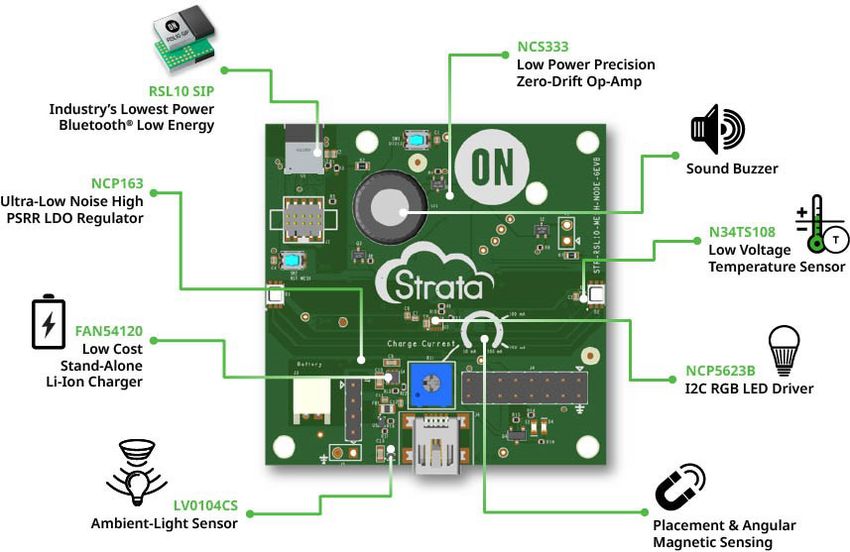
Mesh Networking for Smart Buildings and IoT
  Long Teaser: Bluetooth ) mesh networking promises to accelerate smart buildings, IoT
design, and deployment. This paper explores the basics of Bluetooth mesh networking and
describes how ON Semiconductor is well equipped with the products and development tools
to help speed your design.

  Short Teaser: Explore how Bluetooth mesh networking promises to accelerate smart buildings
and IoT design and deployment.

  Keywords: Mesh, Mesh Networking, Bluetooth, ON Semi, RSL10, ON Semiconductor, BLE,
Bluetooth Low Energy

  Categories: All, Wireless

  Our world is more inter−connected than ever, thanks to the Internet of Things (IoT). As the
demand for greater integration of IoT devices grew, the need for an efficient and reliable
communication standard emerged. The Bluetooth 5.0 specification paved the way for the
introduction of a number of Bluetooth Low Energy networking features, particularly those that
focused on the emerging requirements of IoT applications. Though Bluetooth 5.0 and Bluetooth
Low Energy represented advancements in wireless technology, the inability to support a mesh
topology became a significant limitation as the IoT continued to expand. To overcome this
obstacle, the Bluetooth Special Interest Group (SIG) launched the Bluetooth mesh Device
Properties 1.0 specification, enabling the provisioning of Bluetooth−based interoperable
many−to−many communications. Here, we will explore how mesh networking supports the
integration of IoT devices and a solution that helps engineers accelerate designs requiring
mesh−networking capabilities.

Bluetooth Low Energy Mesh Networking
  Bluetooth Low Energy mesh networks implement a many−to−many (m:m) topology and use
managed flooding to send data. As a result, they do not require any centralized routing or routing
tables like Ethernet networks. Bluetooth Low Energy mesh specifications also offer built−in
security with encryption at multiple layers, so nodes in the network can relay traffic without
needing to be aware of the contents of any messages. The nodes can simply pass them along,
while potential eavesdroppers on the network only see encrypted packets, a significant benefit

                                         www.onsemi.com
                                                2
for network security while preserving design simplicity. A properly placed Bluetooth Low Energy
mesh network can span larger distances than traditional P2P Bluetooth communications as
nodes can perform message passing by relaying packets to a destination node out of range of
the transmitting node. This enables various IoT applications, including connected lighting and
remote sensor monitoring, previously out of range for Bluetooth technology. The mesh
specification allows for up to 32,767 nodes, making it well−suited for deployment in a wide range
of smart buildings and IoT applications with large numbers of individual devices that need to be
connected.
Friend and Low Power Nodes
One of the most exciting features of a Bluetooth Low Energy mesh network is the ability for
certain nodes in the network to operate at significantly reduced power levels − referred to as Low
Power Nodes (LPN) − and improve battery life beyond standard Bluetooth Low Energy devices.
Low Power Nodes optimize power consumption by only waking up from Deep Sleep
intermittently to send and receive data. In order for this to work within a Bluetooth Low Energy
mesh network, a Low Power Node must be located near a Friend node, as it cannot function
without one. The Friend node stores messages destined for the Low Power Node until that node
wakes up to communicate with the rest of the network, at which point, the LPN asks the Friend
node for any pending communications and responds to network activity as needed before going
back into Deep Sleep.
RSL10 Mesh Platform
While designing a new Bluetooth mesh−based product can be a complicated task, there are
tools to help. ON Semiconductor’s RSL10 Mesh Platform is a versatile, easy−to−configure
solution for developing mesh networking applications based on the RSL10 Bluetooth 5 radio.
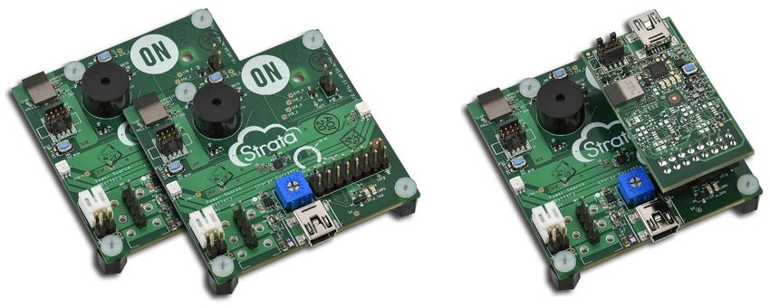
The platform includes two RSL10−based Mesh Nodes and a Strata Gateway, which enables
connectivity to the Strata Developer Studiot and acts as the network provisioner so that nodes
can be securely added and removed (Figure 1). The Strata Gateway supports seamless and
secure connectivity to the Strata Developer Studio. This cloud−connected software enables
provisioning of additional mesh networks and firmware−over−the−air (FOTA) updates. Using
the virtual workspaces for common mesh networking examples, including a smart office and
smart home, developers can access sensor data and trigger settings such as signal strength,
ambient light, battery, temperature, and node connections for every node within the network in
the Strata basic view. An advanced view allows the user to view several code examples.
www.onsemi.com
3Figure 1. The RSL10 Mesh Platform Kit Consists of Two RSL10 Mesh Nodes
and a Strata Gateway
With the RSL10 Mesh Platform, engineers can easily implement ultra−low−power mesh
networking, using Bluetooth Low Energy technology, and move quickly toward full deployment.
Optimized for smart home, building automation, industrial IoT, remote environment monitoring,
and asset tracking and monitoring applications, this multi−faceted solution has all the essential
elements needed for developing and deploying a mesh network. Alongside the RSL10
System−in−Package (RSL10 SIP), the Mesh Nodes feature multiple environmental sensors for
monitoring temperature, ambient light, and magnetic field detection. The nodes also include
a 2.3 kHz tone indicator, a connector for vibration buzzers, and light dimming and alarm
capabilities (Figure 2).
Figure 2. RSL10 Mesh Nodes Consist of the Features Required for
Developing and Deploying a Mesh Network
www.onsemi.com
4With its best−in−class ultra−low−power consumption, the RSL10 Mesh Platform is perfectly
suited to demonstrate the Low Power Node capabilities of Bluetooth Low Energy mesh.
ON Semiconductor’s Bluetooth Low Energy mesh roadmap highlights this by enabling
Bluetooth Low Energy mesh Low Power Node functionality on existing RSL10−SENSE−GEVK
and RSL10−COIN−GEVB evaluation boards and integrating Friend and Low Power Node
behavior into the Mesh Platform Strata user interface.
RSL10 SIP
The RSL10 SIP enables advanced wireless features while optimizing system size and battery
life. It is designed for applications using as low as 1.2 V batteries, and supports a voltage supply
range between 1.1 and 3.3 V without external components. The highly−integrated radio SoC
features a dual−core architecture and a 2.4 GHz transceiver, providing the flexibility to support
Bluetooth Low Energy and 2.4 GHz custom protocols. The RSL10 is the industry’s lowest power
consumption Bluetooth Low Energy System on Chip; in Deep Sleep Mode only consuming
62.5 nW and only 7 mW receive power in Receive Mode. The RSL10 also has impressive
EEMBC® ULPMarkt scores (1090 ULPMark CP @ 3 V; 1260 @ 2.1 V).
N34TS108
N34TS108 is a digital−output temperature sensor with a dynamically−programmable limit
window, and under− and over temperature alert functions. These features provide optimized
temperature control without the need of frequent temperature readings by the controller or
application processor. The N34TS108 features SMBus and two−wire interface compatibility,
and allows up to four devices on one bus with the SMBus alert function. The N34TS108 is ideal
for thermal management optimization in a variety of consumer, computer, and environmental
applications. The device is specified over a temperature range of –40°C to +125°C.
FAN54120
The FAN54120 is a USB−compatible single−cell, linear Li−Ion battery charger with “Power
Back” Capability, It supports dead battery revival, pre−charge, fast charge, and float charge
states. Fast charging current (IFAST) is set with an external resistor. Pre−charge (IPRE) and
charge complete (ICHGEND) currents are factory set at IFAST/5.2 and IFAST/10, respectively.
An open−drain (“STAT”) pin provides charge and/or fault status indication. The “Power Back”
enables to power accessories from the battery.
NCP5623B
The NCP5623B mixed analog circuit is a triple output LED driver dedicated to the RGB
illumination or backlight LCD display. The built in DC to DC converter is based on a high efficient
charge pump structure with operating mode 1x and 2x. It provides a 94 percent peak efficiency.
The tiny package makes the device suitable for room limited portable applications.
www.onsemi.com
5LV0104CS
LV0104CS is a photo IC for ambient light sensor which has the characteristics of spectral
response similar to that of human eyes. It is suitable for the applications like mobile phone (for
Digital−TV, One−segment), LCD−TV, laptop computer, PDA, DSC and Camcorder.
NCP163
The NCP163 is an LDO (Low Dropout Regulator) capable of supplying 250 mA output current.
Designed to meet the requirements of RF and analog circuits, the NCP163 device provides low
noise, high PSRR, low quiescent current, and very good load/line transients. The device is
designed to work with a 1 mF input and a 1 mF output ceramic capacitor. It is available in two
thickness ultra−small 0.35P, 0.65 mm x 0.65 mm Chip Scale Package (CSP), XDFN−4 0.65P,
1 mm x 1 mm and in TSOP5 packages
NCS333
The NCS333 is a precision op amp with very low input offset voltage (10 mV max) and
near−zero drift over time and temperature. This high precision, low quiescent current amplifiers
has high impedance inputs with a common−mode range 100 mV beyond the rails as well as
rail−to−rail output swing within 50 mV of the rails. The NCS333 features a wide supply range
from 1.8 V to 5.5 V (±0.9 V to ±2.75 V for dual supplies). The NCS333 family exhibits
outstanding CMRR without the crossover associated with traditional complementary input
stages. This design results in superior performance for driving analog−to−digital converters
(ADCs) without degradation of differential linearity.
Conclusion
Bluetooth mesh networking opened up the opportunity for the development of many new IoT
products. The mesh specification allows for up to 32,767 nodes, making it well−suited for
deployment in a wide range of smart buildings and IoT applications requiring large numbers of
individual devices to be connected. Using the ON Semiconductor RSL10 Mesh Platform,
engineers can accelerate mesh−networking development, so that nodes can be more rapidly
deployed while pushing the performance envelope in terms of range, resiliency, and power
budget.
www.onsemi.com
6Bluetooth and the Bluetooth logo are registered trademarks of Bluetooth SIG.
Strata Developer Studio is a trademark of Semiconductor Components Industries, LLC (SCILLC) or its subsidiaries in the United States and/or other
countries.
All other brand names and product names appearing in this document are registered trademarks or trademarks of their respective holders.
ON Semiconductor and are trademarks of Semiconductor Components Industries, LLC dba ON Semiconductor or its subsidiaries in the United States and/or other countries.
ON Semiconductor owns the rights to a number of patents, trademarks, copyrights, trade secrets, and other intellectual property. A listing of ON Semiconductor’s product/patent
coverage may be accessed at www.onsemi.com/site/pdf/Patent−Marking.pdf. ON Semiconductor reserves the right to make changes without further notice to any products herein.
ON Semiconductor makes no warranty, representation or guarantee regarding the suitability of its products for any particular purpose, nor does ON Semiconductor assume any liability
arising out of the application or use of any product or circuit, and specifically disclaims any and all liability, including without limitation special, consequential or incidental damages.
Buyer is responsible for its products and applications using ON Semiconductor products, including compliance with all laws, regulations and safety requirements or standards,
regardless of any support or applications information provided by ON Semiconductor. “Typical” parameters which may be provided in ON Semiconductor data sheets and/or
specifications can and do vary in different applications and actual performance may vary over time. All operating parameters, including “Typicals” must be validated for each customer
application by customer’s technical experts. ON Semiconductor does not convey any license under its patent rights nor the rights of others. ON Semiconductor products are not
designed, intended, or authorized for use as a critical component in life support systems or any FDA Class 3 medical devices or medical devices with a same or similar classification
in a foreign jurisdiction or any devices intended for implantation in the human body. Should Buyer purchase or use ON Semiconductor products for any such unintended or unauthorized
application, Buyer shall indemnify and hold ON Semiconductor and its officers, employees, subsidiaries, affiliates, and distributors harmless against all claims, costs, damages, and
expenses, and reasonable attorney fees arising out of, directly or indirectly, any claim of personal injury or death associated with such unintended or unauthorized use, even if such
claim alleges that ON Semiconductor was negligent regarding the design or manufacture of the part. ON Semiconductor is an Equal Opportunity/Affirmative Action Employer. This
literature is subject to all applicable copyright laws and is not for resale in any manner.
PUBLICATION ORDERING INFORMATION
LITERATURE FULFILLMENT: TECHNICAL SUPPORT
Email Requests to: orderlit@onsemi.com North American Technical Support: Europe, Middle East and Africa Technical Support:
Voice Mail: 1 800−282−9855 Toll Free USA/Canada Phone: 00421 33 790 2910
ON Semiconductor Website: www.onsemi.com Phone: 011 421 33 790 2910 For additional information, please contact your local Sales Representative
◊ www.onsemi.com
7You can also read