MINI EVALUATION BOARD USER MANUAL - FOR RADIO MODULES - FEBRUARY 25, 2021 - Würth Elektronik
←
→
Page content transcription
If your browser does not render page correctly, please read the page content below
M INI   EVALUATION BOARD USER MANUAL

                F OR RADIO MODULES

         EV order code     Module order code   Product Name
         2611069024001     2611011024000       Proteus-III
         2611119024011     2611011024010       Proteus-III-SPI
         2611079021001     2611011021000       Thyone-I

                            V ERSION 1.2

                         F EBRUARY 25, 2021
***************
MUST READ
Check for firmware updates

Before using the product make sure you use the most recent firmware version, data sheet
and user manual. This is especially important for Wireless Connectivity products that were
not purchased directly from Würth Elektronik eiSos. A firmware update on these respective
products may be required.

We strongly recommend to include in the customer system design, the possibility for a
firmware update of the product.
Revision history

 Manual    HW
                     Notes                                                   Date
 version   version

 1.0       1.0          • Initial version                                    October 2020

                        • Order number is updated in the schematic 3.7.

                        • Bill of materials is added in chapter 3.9.

 1.1       1.0          • LFXO crystal part number is updated in chapter     January 2021
                          3.6.5.
                        • Input capacitance variables CXC1 and CXC2 are
                          changed to CXL1 and CXL2 respectively 3.6.5.

                        • Added information on Proteus-III-SPI radio
                          module
 1.2       1.0                                                               February 2021
                        • Chapter LFXO crystal is updated.

Mini evaluation board user manual version 1.2                              © February 2021
www.we-online.com/wireless-connectivity                                                 1
Abbreviations and abstract
Abbreviation
Name Description
EV Evaluation
ESD Electro Static Discharge
Future Technology
FTDI
Devices International
GND Ground
HIGH High signal level
JTAG Joint Test Action Group
LED Light Emitting Diode
LFCLK Low frequency clock
Low frequency crystal
LFXO
oscillator
LOW Low signal level
NFC Near Field Communication
OTA Over the air
PC Personal Computer
PCB Printed Circuit Board
Describes everything relating to the wireless
RF Radio frequency
transmission.
SMA SubMiniature version A
SPI Serial Peripheral Interface
SWD Serial Wire Debug
THT Through-hole technology
Universal Asynchronous Receiver Transmitter allows
Universal Asynchronous
UART communicating with the module of a specific
Receiver Transmitter
interface.
USB Universal Serial Bus
VDD Voltage Drain Drain Supply voltage
Mini evaluation board user manual version 1.2 © February 2021
www.we-online.com/wireless-connectivity 2Contents
1 Supported radio modules 5
2 Functional description 7
2.1 Taking into operation - PC (Proteus-III/Thyone-I only) . . . . . . . . . . . . . 7
2.2 Taking into operation - Host controller . . . . . . . . . . . . . . . . . . . . . 8
3 Development board 9
3.1 Block diagram . . . . . . . . . . . . . . . . . . . . . . . . . . . . . . . . . . . 9
3.2 Additional assembly . . . . . . . . . . . . . . . . . . . . . . . . . . . . . . . 10
3.3 Connectors and ports . . . . . . . . . . . . . . . . . . . . . . . . . . . . . . 12
3.3.1 P1, P2, P4: Module access pins . . . . . . . . . . . . . . . . . . . . 13
3.3.2 P3: TTL-232R-3V3 FTDI cable connector . . . . . . . . . . . . . . 14
3.3.3 P5, P6: Alternative power supply connection . . . . . . . . . . . . . 14
3.3.4 JTAG Debugging Interface . . . . . . . . . . . . . . . . . . . . . . . 14
3.3.5 SMA . . . . . . . . . . . . . . . . . . . . . . . . . . . . . . . . . . . 15
3.4 Jumpers . . . . . . . . . . . . . . . . . . . . . . . . . . . . . . . . . . . . . . 16
3.4.1 I_Meas: Current measurement . . . . . . . . . . . . . . . . . . . . 17
3.4.2 JP2: Operation mode . . . . . . . . . . . . . . . . . . . . . . . . . . 18
3.4.3 JP3: Boot mode . . . . . . . . . . . . . . . . . . . . . . . . . . . . . 18
3.5 Reset button . . . . . . . . . . . . . . . . . . . . . . . . . . . . . . . . . . . 19
3.6 Function blocks . . . . . . . . . . . . . . . . . . . . . . . . . . . . . . . . . . 20
3.6.1 Power supply . . . . . . . . . . . . . . . . . . . . . . . . . . . . . . 20
3.6.1.1 Connector P3, power supply through TTL-232R-3V3 . . . . . . 20
3.6.1.2 Connector P3, power supply through external source . . . . . . 20
3.6.1.3 Connectors P5 and P6, power supply through external source . 20
3.6.2 UART / USB . . . . . . . . . . . . . . . . . . . . . . . . . . . . . . . 21
3.6.3 UART direct . . . . . . . . . . . . . . . . . . . . . . . . . . . . . . . 21
3.6.4 SPI direct . . . . . . . . . . . . . . . . . . . . . . . . . . . . . . . . 21
3.6.5 LFXO crystal . . . . . . . . . . . . . . . . . . . . . . . . . . . . . . 21
3.6.5.1 LFXO Design guidelines . . . . . . . . . . . . . . . . . . . . . . 23
3.6.6 Programming interface . . . . . . . . . . . . . . . . . . . . . . . . . 23
3.7 Schematic . . . . . . . . . . . . . . . . . . . . . . . . . . . . . . . . . . . . . 24
3.8 Layout . . . . . . . . . . . . . . . . . . . . . . . . . . . . . . . . . . . . . . . 25
3.9 Bill of materials . . . . . . . . . . . . . . . . . . . . . . . . . . . . . . . . . . 27
4 Regulatory compliance information 28
4.1 European Conformity . . . . . . . . . . . . . . . . . . . . . . . . . . . . . . . 28
4.2 FCC . . . . . . . . . . . . . . . . . . . . . . . . . . . . . . . . . . . . . . . . 28
4.3 Exemption clause . . . . . . . . . . . . . . . . . . . . . . . . . . . . . . . . . 28
5 Important notes 29
5.1 General customer responsibility . . . . . . . . . . . . . . . . . . . . . . . . . 29
5.2 Customer responsibility related to specific, in particular safety-relevant ap-
plications . . . . . . . . . . . . . . . . . . . . . . . . . . . . . . . . . . . . . 29
5.3 Best care and attention . . . . . . . . . . . . . . . . . . . . . . . . . . . . . 29
5.4 Customer support for product specifications . . . . . . . . . . . . . . . . . . 29
5.5 Product improvements . . . . . . . . . . . . . . . . . . . . . . . . . . . . . . 30
5.6 Product life cycle . . . . . . . . . . . . . . . . . . . . . . . . . . . . . . . . . 30
5.7 Property rights . . . . . . . . . . . . . . . . . . . . . . . . . . . . . . . . . . 30
Mini evaluation board user manual version 1.2 © February 2021
www.we-online.com/wireless-connectivity 35.8 General terms and conditions . . . . . . . . . . . . . . . . . . . . . . . . . . 30 6 Legal notice 31 6.1 Exclusion of liability . . . . . . . . . . . . . . . . . . . . . . . . . . . . . . . . 31 6.2 Suitability in customer applications . . . . . . . . . . . . . . . . . . . . . . . 31 6.3 Trademarks . . . . . . . . . . . . . . . . . . . . . . . . . . . . . . . . . . . . 31 6.4 Usage restriction . . . . . . . . . . . . . . . . . . . . . . . . . . . . . . . . . 31 7 License terms 33 7.1 Limited license . . . . . . . . . . . . . . . . . . . . . . . . . . . . . . . . . . 33 7.2 Usage and obligations . . . . . . . . . . . . . . . . . . . . . . . . . . . . . . 33 7.3 Ownership . . . . . . . . . . . . . . . . . . . . . . . . . . . . . . . . . . . . . 34 7.4 Firmware update(s) . . . . . . . . . . . . . . . . . . . . . . . . . . . . . . . . 34 7.5 Disclaimer of warranty . . . . . . . . . . . . . . . . . . . . . . . . . . . . . . 34 7.6 Limitation of liability . . . . . . . . . . . . . . . . . . . . . . . . . . . . . . . . 34 7.7 Applicable law and jurisdiction . . . . . . . . . . . . . . . . . . . . . . . . . . 35 7.8 Severability clause . . . . . . . . . . . . . . . . . . . . . . . . . . . . . . . . 35 7.9 Miscellaneous . . . . . . . . . . . . . . . . . . . . . . . . . . . . . . . . . . . 35 Mini evaluation board user manual version 1.2 © February 2021 www.we-online.com/wireless-connectivity 4
1 Supported radio modules
The evaluation board described in this manual can be used to evaluate the following prod-
ucts:

 Order code         Product Name         Description
                                         Bluetooth® LE 5.1 radio module with smart
 2611011024000      Proteus-III
                                         antenna configuration
                                         Variant of the Proteus-III radio module providing
 2611011024000      Proteus-III-SPI
                                         a SPI instead of an UART for host connection
                                         2.4GHz proprietary radio module with smart
 2611011021000      Thyone-I
                                         antenna configuration

           Order code          Product Name
           2611069024001       Mini EV Board Proteus-III
           2611119024011       Mini EV Board Proteus-III-SPI
           2611079021001       Mini EV Board Thyone-I
                                   Table 1: Compatibility

                                  Figure 1: Product image

      Content 2611069024001                                          Quantity
      Mini Evaluation board with Proteus-III On-board PCB
                                                                     1
      Antenna connection
      Packaging: ESD safe cover                                      1
                        Table 2: Content Mini EV Board Proteus-III

Mini evaluation board user manual version 1.2                              © February 2021
www.we-online.com/wireless-connectivity                                                      5
Content 2611119024011 Quantity
Mini Evaluation board with Proteus-III-SPI On-board PCB
1
Antenna connection
Packaging: ESD safe cover 1
Table 3: Content Mini EV Board Proteus-III-SPI
Content 2611079021001 Quantity
Mini Evaluation board with Thyone-I On-board PCB
1
Antenna connection
Packaging: ESD safe cover 1
Table 4: Content Mini EV Board Thyone-I
Mini evaluation board user manual version 1.2 © February 2021
www.we-online.com/wireless-connectivity 62 Functional description
The mini evaluation board is an intuivitive, application oriented and cost effective version
of the evaluation kit. It offers the user the possibility to develop hard- and software for the
corresponding radio module.
By default, the mini evaluation board is not assembled with connectors and pinheaders. The
necessary components shall be assembled by the user based on the need and application.
The mini evaluation board is intended for experienced developers, as additional accessories
and basic soldering skills are necessary to take the board into operation.
Accessories required:
• Additional assembly components listed in the table 5.
Connector kit article number: 699100.
• Soldering equipment
• (optional) TTL-232R-3V3 FTDI cable in case of Proteus-III or Thyone-I
For the connection to a micro controller or PC the evaluation board is equipped with place-
holders for standard 2.54mm headers which is connected to the pins of the radio module.
Pin headers can be soldered to the placeholders to access the module pins. Jumpers allow
to set the module into defined modes.
In case of Proteus-III and Thyone-I, the mini evaluation board can be connected to an USB
port of a PC using TTL-232R-3V3 FTDI cable.
2.1 Taking into operation - PC (Proteus-III/Thyone-I only)
To take the mini evaluation board into operation using a PC, additional assembly as de-
scribed in the chapter 3.2 is necessary.
The corresponding FTDI driver package (www.ftdichip.com/Drivers/VCP.htm) has to be in-
stalled on the PC.
The installation guidelines shall be followed:
(https://www.ftdichip.com/Support/Documents/InstallGuides.htm)
The TTL-232R-3V3 FTDI cable shall be connected to the connector P3 of the evaluation
board. It is important that the VDD is stable and able to reliably supply the module’s static
and peak current consumption as specified by the module manual.
Incorrect orientation of TTL-232R-3V3 FTDI cable will damage the RF module.
The next step is to connect the evaluation board to the PC using the TTL-232R-3V3 FT-
DI cable. In that way a COM port can be detected and installed on the PC. In the device
Mini evaluation board user manual version 1.2 © February 2021
www.we-online.com/wireless-connectivity 7manager the COM port name of the TTL-232R-3V3 FTDI cable can be found. A COM port shall appear for example: "COM12" in Windows systems or "/dev/ttyUSB0" in Linux systems. The WE-SmartCommander or any other serial terminal program (like hterm for Windows) has to be run and the corresponding COM port has to be opened using the default settings of the mounted radio module. After the module is powered through the TTL-232R-3V3 FTDI cable or an alternative power supply, the reset button should be pressed to ensure a clean start-up of the module. The detailed module specific quick start instructions can be found in the corresponding user manual. 2.2 Taking into operation - Host controller To take the mini evaluation board into operation using a host controller, additional assembly as described in the chapter 3.2 is necessary. An external power supply shall be connected to the evaluation board. The power supply op- tion 3 or 4 from the table 17 shall be used. It is important that the VDD is stable and able to reliably supply the module’s static and peak current consumption as specified by the module manual. The next step is to connect the communication lines of the module to the host controller. The headers P1, P2 and P3 can be used to connect the module pins and host. The detailed module specific quick start instructions can be found in the corresponding user manual. Feel free to check our youtube channel for video tutorials, hands-ons and webinars relating to our products: www.youtube.com/user/WuerthElektronik/videos Mini evaluation board user manual version 1.2 © February 2021 www.we-online.com/wireless-connectivity 8
3 Development board
3.1 Block diagram

                                                                                50Ω port to       SMA Connector
                Mini evaluation                    2.54mm pin headers           λ/4 antenna            THT
                                                 (Access to module pins)
                board
                     Current
                  Measurement /
                   Solderbridge                                   RF Filter &       Internal
                           3.3V                                  50Ω matching       Antenna
                    5V to 3.3V
                     Voltage
                    regulator
                                                            Radio module
                           5V
                    2.54mm
                   pin header     UART or SPI
                    P3 (1X6)      (3.3V logic)
                                                  2.54mm pin           Reset
                                                                                       LEDs
                                                    header             Button
                                                   Connector
                                                  (VDD, GND)

                                                   Alternate
                                                  power supply
                                                     (3.3V)

                                    Figure 2: Block diagram

Mini evaluation board user manual version 1.2                                                  © February 2021
www.we-online.com/wireless-connectivity                                                                       9
3.2 Additional assembly
Figure 3: Additional assembly
Mini evaluation board user manual version 1.2 © February 2021
www.we-online.com/wireless-connectivity 10The table 5 lists the additional assembly components for the evaluation board. All the com-
ponents listed in the table 5 are THT components.
Placeholder Function Pins WE Article Number
I_Meas Current measurement 1X2 61300211121
JP2 Boot mode set 1X2 61300211121
JP3 Operation mode set 1X2 61300211121
JTAG JTAG Debug interface 2X10 61302021121
P1 Access to module pins 1X6 61300611121
P2 Access to module pins 1X7 61300711121
TTL-232R-3V3 FTDI cable
P3 1X6 61300411121
connection / Access to module pins
P4 Access to module pins 1X4 61300411121
P5 Ground connection 1X3 61300311121
P6 3.3V Connection 1X3 61300311121
SMA External antenna connection 1X4 60312002114503
2.54mm Jumpers I_Meas, JP2, JP3 1X3 60900213421
Table 5: Additional assembly components
Connector kit containing all the components listed in the table 5 is available.
Connector kit article number: 699100.
Based on the necessity the required components shall be assembled.
Holes with 2mm diameter on all the four corners are available for Spacer or
Standoff connections
Mini evaluation board user manual version 1.2 © February 2021
www.we-online.com/wireless-connectivity 113.3 Connectors and ports
Figure 4: Connectors
Mini evaluation board user manual version 1.2 © February 2021
www.we-online.com/wireless-connectivity 123.3.1 P1, P2, P4: Module access pins
P1 nRF52840 Function
1 P0.18 RESET
2 SWDIO SWDIO
3 SWCLK SWCLK
4 GND
Table 6: Pin header P1
P2 nRF52840 Function
1 P0.22 BUSY
2 P0.09 B1, RSVD
3 P0.10 B2, RSVD
4 P0.23 B3, RSVD
5 P1.00 B4, RSVD
6 P0.21 B5, RSVD
7 P0.07 B6, RSVD
Table 7: Pin header P2
P4 nRF52840 Function
1 P0.00/XL1 LED1
2 P0.01/XL2 LED2
3 P0.03 WAKE_UP / SPI_INT
4 GND
Table 8: Pin header P4
Mini evaluation board user manual version 1.2 © February 2021
www.we-online.com/wireless-connectivity 133.3.2 P3: TTL-232R-3V3 FTDI cable connector
P3 nRF52840 Function
1 GND
2 P0.11 /RTS (SPI_CS)
3 5V
4 P1.09 URXD (SPI_MOSI)
5 P1.08 UTXD (SPI_MISO)
6 P0.12 /CTS (SPI_SCLK)
Table 9: Pin header P3
In case of Proteus-III or Thyone-I, the pin header P3 is used to connect the
TTL-232R-3V3 FTDI cable. P3 can also be used for direct host connection.
3.3.3 P5, P6: Alternative power supply connection
P5 Connection
1,2,3 GND
Table 10: Pin header P5
P6 Connection
1,2,3 3.3V power supply
Table 11: Pin header P6
All the information related to the power supply are described in the chapter 3.6.1.
3.3.4 JTAG Debugging Interface
JTAG nRF52840 Function
1 VDD
7 SWDIO SWDIO
9 SWCLK SWCLK
15 P0.18 RESET
4,6,8,10,12,14,16,18,20 GND
2,3,5,11,13,17,19 Not Connected
Table 12: JTAG debugging interface
Mini evaluation board user manual version 1.2 © February 2021
www.we-online.com/wireless-connectivity 143.3.5 SMA
SMA connector is used to connect an external antenna.
The 2.4 GHz antenna Himalia (2600130021) is a perfect match.
SMA Connection
Inner Module RF pin
Outer 4 x GND
Table 13: Pin header SMA
In order to use an external SMA antenna, 22 pF capacitor (0402) on position
C1 shall be populated. C2, C8, C11 and C12 should be left unpopulated.
Optional: Experts have the possibility to use C11, C1 and C8 for additional
filtering or fine tuning.
Figure 5: Capacitor connection to external antenna
In order to use the internal PCB antenna of the module, a 2.4 nH inductor
(0402) on position C2 and a 0.3 pF capacitor (0402) on position C12 shall be
populated respectively. C1, C8 and C11 should be left unpopulated.
Figure 6: Capacitor connection to internal antenna
Mini evaluation board user manual version 1.2 © February 2021
www.we-online.com/wireless-connectivity 153.4 Jumpers
Figure 7: Jumpers
Mini evaluation board user manual version 1.2 © February 2021
www.we-online.com/wireless-connectivity 163.4.1 I_Meas: Current measurement
By default, I_Meas pin header is not assembled and solder bridge near the I_Meas jumper
SJ2 is connected.
The power LED is on the VDD line of the module and shows that the module is sourced. To
measure module power consumption and to disconnect the power LED, the resistor R4 shall
be desoldered.
If the module is sourced through the P3 connector, the current consumption of the module
can be measured on the I_Meas pin header. For this measurement, the solder bridge SJ2
shall be disconnected using a cutter and a current meter shall be connected to the I_Meas
pin header. For normal operation a jumper is set on the I_Meas pin header.
I_Meas Function
1 3.3V LDO Output
2 VDD
Table 14: Pin header I_Meas
Figure 8: Current measurement
By default the solder bridge SJ2 is connected. For power consumtion mea-
surement, the solder bridge shall be disconnected using a cutter and resisto
R4 shall be desoldered.
Current measurement using I_Meas jumper is possible only if the module is
powered through connector P3.
Mini evaluation board user manual version 1.2 © February 2021
www.we-online.com/wireless-connectivity 173.4.2 JP2: Operation mode
By default, JP2 is not assembled. If Jumper JP2 is set during power up or reset, the module
starts in transparent mode. For command mode operation, JP2 shall be left open during
power up or reset.
JP2 nRF52840 Function
1 VDD
2 P0.19 MODE_1
Table 15: Pin header JP2
3.4.3 JP3: Boot mode
By default, JP3 is not assembled. If jumper JP3 is set during power up, the module starts in
bootloader mode. For command mode operation the module JP3 shall be left open during
power up.
• For Proteus-III (2611011024000) and Proteus-III-SPI (2611011024010)
module, bootloader mode allows only over the air (OTA) firmware update.
• For Thyone-I module (2611011021000), bootloader mode allows
firmware update only via UART.
JP3 nRF52840 Function
1 GND
2 P0.02 BOOT
Table 16: Pin header JP3
Mini evaluation board user manual version 1.2 © February 2021
www.we-online.com/wireless-connectivity 183.5 Reset button
Figure 9: Buttons
On IC level the active low reset input is configured with a pull up resistor. The module
provides a /RESET pin that is connected to this button so that the module can be restarted
properly. Please refer to the module specific manual for detailed information.
Mini evaluation board user manual version 1.2 © February 2021
www.we-online.com/wireless-connectivity 193.6 Function blocks
3.6.1 Power supply
The mini evaluation board can be powered either by TTL-232R-3V3 cable or by an external
power supply. The table 17 lists the connection for different power supply options.
I_Meas
I_Meas Solder Supported
Nr. Power supply Connector current
jumper bridge modules
meas.
TTL-232R-3V3 Proteus-III /
1 P3 Open Connected No
cable Thyone-I
TTL-232R-3V3 Proteus-III /
2 P3 Set disconnected Yes
cable Thyone-I
P3 Pin-3 (5V)
3 External supply P3 Pin-1 Set disconnected Yes All
(GND)
P5 (GND) P6
4 External supply Open Open No All
(VDD)
Table 17: Power supply option
By default solder bridge is connected and pin headers are not assembled.
3.6.1.1 Connector P3, power supply through TTL-232R-3V3
The evaluation board can be sourced by TTL-232R-3V3 cable through P3 connector. TTL-
232R-3V3 cable powers the board with 5V supply. The integrated voltage regulator regulates
the connected voltage 5V down to 3.3V and supplies the remaining parts of the circuit. If the
module is sourced, the power Power LED lights up.
3.6.1.2 Connector P3, power supply through external source
The evaluation board can be sourced by an external power supply through the P3 connector
Pin-3 (5V) and P3 Pin-1 (GND). If the module is sourced, the power Power LED lights up.
3.6.1.3 Connectors P5 and P6, power supply through external source
The development board can be sourced by an external power supply through the P5 (GND)
and P6 (3.3V) connector. If the module is sourced, the power Power LED lights up.
To use this option I_Meas jumper and SJ2 shall be left open.
Mini evaluation board user manual version 1.2 © February 2021
www.we-online.com/wireless-connectivity 203.6.2 UART / USB
The TTL-232R-3V3 cable is used for USB/UART connection between PC and the evaluation
board. The IO level of the TTL-232R-3V3 cable is 3.3V. Using the FTDI-driver the PC will
show a virtual COM-Port which can be used to communicate with the module.
3.6.3 UART direct
If a micro-controller is to be connected to the module, use the P3 connector. The UART of
the host can be directly connected to P3 (Pins are labelled on the evaluation board). The
module RXD line must be handled accordingly by your host (i.e. pulled up while inactive and
during module boot-up).
Beware of IO level compatibility. The host must obey the values stated in the module’s
manual. Especially the IO level restrictions must be implemented by a host system (i.e.
using a level shifter to use the allowed IO levels).
3.6.4 SPI direct
If a micro-controller is to be connected to the module, use the P3 connector and WAKE_UP/SPI_INT
(P4 pin 3). The SPI of the host can be directly connected to these pins. For easy orientation
the pins are labelled on the evaluation board with its functions.
Beware of IO level compatibility. The host must obey the values stated in the module’s
manual. Especially the IO level restrictions must be implemented by a host system (i.e.
using a level shifter to use the allowed IO levels).
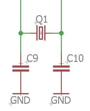
3.6.5 LFXO crystal
For higher LFCLK accuracy (better than ±250ppm) a low frequency crystal oscillator of
32.768kHz (LFXO) shall be used. A crystal, 3.2 ×1.6mm package, for example 830009706,
can be placed on the evaluation board to position Q1. The needed load capacitance can be
reached with capacitors C9 and C10, 0402 package.
nRF52840 pin P0.00/XL1 and P0.01/XL12 are connected to module pad LED_1 and LED_2
respectively. If an LFXO is mounted to the EV board the solder bridge SJ1 and SJ3 shall
be disconnected using a cutter, therefore the LED1 and LED2 function is no longer available.
For standard firmware the external crystal is not needed. To enable use of the
LFXO a custom firmware is required.
By default the LED_1 and LED_2 functions of the module are used.
Mini evaluation board user manual version 1.2 © February 2021
www.we-online.com/wireless-connectivity 21Figure 10: LFXO assembly
To use the LFXO function, the two solder bridges near the LFXO place holder
shall be disconnected using a cutter.
The input capacitance of the pad LED_1 and LED_2 are 4 pF. The values of C9 and C10
can be calculated as follows.
The load capacitance of LFXO is given by
C9l ∗ C10l
Cl = (1)
C9l + C10l
If C9l = C10l = C, then
C
Cl = (2)
2
whereas,
C9 = C − CXL1 − CP CB (3)
C10 = C − CXL2 − CP CB (4)
Cl = Load capacitance of LFXO crystal.
CXL1 = Input capacitance of Pad LED_1 (4 pF)
CXL2 = Input capacitance of Pad LED_2 (4 pF)
CP CB = Parasitic capacitance of PCB Parasitic capacitance of the PCB can vary depending
on design and track length. It can vary from 0.5 pF to 2 pF.
For the crystal 830009706 with load capacitance of 9 pF and parasitic capacitance of 2 pF.
The value of C9 and C10 results in 12 pF which was also tested on the evaluation board.
Depending on parasitic capacitance of PCB, a capacitance of 12 pF may be a good starting
value for C9 and C10.
Mini evaluation board user manual version 1.2 © February 2021
www.we-online.com/wireless-connectivity 223.6.5.1 LFXO Design guidelines
1. LFXO shall be placed away from high frequency components and traces.
2. The ground connection for the load capacitor shall be short using ground vias.
3. The crystal shall be placed close to the module.
4. PCB traces between module and the crystal shall be kept short.
5. Load capacitors shall be low leakage and temperature stable (NPO or COG) type.
6. The differential traces shall be kept to the same length.
7. Ground area shall be placed under crystal and connected to the main ground plane.
8. Open traces to the pins shall be avoided to reduce parasitic capacitance and coupling
effects.
9. Ground area shall be used between the crystal traces and other PCB traces for better
decoupling.
3.6.6 Programming interface
The evaluation board provides a place holder for 2×10 pin connector. It can be used to con-
nect directly to a JTAG flash adapter used for development. Please take care of the correct
mounting of the flash adapter. The recommended flash adapter is one of the "Segger J-Link"
family.
Mini evaluation board user manual version 1.2 © February 2021
www.we-online.com/wireless-connectivity 23TTL-232R-3V3 cable connector Debug-interface
RF-module (3.3 I/O Logic level) JTAG
GND VDD_RF 1 2
P3 3 4
GND
PROTEUS-III/THYONE-I 1 GND 5 6
C12 261101102x000 P0.11/RTS 2 CTS SWDIO 7 8
GND
0.3pF C2 5V0 3 VCC SWDCLK 9 10
C1 2.4nH P1.09/URXD 4 TXD 11 12
n.m. 1 ANT GND
18 P1.08/UTXD 5 RXD 13 14
SMA 5 17 6 16
3.7 Schematic
n.m.
2 RF WAKE_UP P0.12/CTS RTS P0.18/RESET15
GND 3 GND /CTS
16 17 18
1*4 C11 C8 SWDCLK4 SWDCLK /RTS
15 n.m. 19 20
n.m. n.m. SWDIO 5 SWDIO URXD
14 External quartz assembly
P0.18/RESET 6 /RESET UTXD
13 (Optional) n.m.
BOOT 7 BOOT LED_2
12 C10
GND GND GND VDD 8 VDD LED_1
11 n.m. GND
MODE_1 9 MODE_1 BUSY
10 LED2
GND
Q1 External power supply 3.3V
C9
B1
B2
B3
B4
B5
B6
n.m. n.m. 3.3V Ground
B1
B2
B3
B4
B5
B6
LED1
P6 P5
GND
2
2
3 VDD_RF 3 GND
VDD_RF 2 VDD_RF 2 GND
SJ1
SJ3
n.m.
n.m.
C7 C6 Pin headers to module pins 1 VDD_RF 1 GND
1
1
L1
P2
100nF 1µF BUSY 1 n.m. n.m.
B1 2
B2 3
7427927311
GND GND B3 4 n.m.
B4 5 LED1 R1
www.we-online.com/wireless-connectivity
B5 6 yellow
B6 7 1K5R LED_1S
LED1
GND
P4
LED_1S 1
Mini evaluation board user manual version 1.2
LED_2S 2 LED2
3 R2
WAKE_UP n.m. blue
4 1K5R
GND LED_2S
LED2
GND
Operation mode Jumper Bootloader Jumper
JP2 JP3 P1
VDD_RF 1 GND 1 P0.18/RESET 1 LED3 R3
MODE_1 2 BOOT 2 SWDIO 2 green
3 1K5R
SWDCLK n.m. BUSY
n.m. n.m. GND 4 LED3
GND
Figure 11: Schematic sheet
Internal LDO Power-supply O1 O2 O3
n.m. Solder jumper
VDD_INT SJ2 Fiducial Mark Fiducial Mark Fiducial Mark
1 2
T1 VERTRAULICH/CONFIDENTIAL
n.m. Reset button TITLE:
OUT
5V0 5V VDD_RF
1
2
IN OUT
C5 C4 C3 P0.18/RESET
JP1
n.m.
L2
ADJ R4 1 3 26110x902xxxx-HW-V1.0
10KR
100nF IC1 100nF 1µF
TLV1117LV Current Measurement S1 PROJECT: 2611069024001
GND GND GND GND Jumper 430152043826 2611079021001
2611119024011
7427927311
2 4
red
LED_POWER
DESCRIPTION DATE NAME DATE NAME REV:
DRAWN 2/22/2021 9:11:15 AM
GND CHECK SHEET
GND APPVD 1/1
FILE NAME: 26110x902xxxx-HW-V1.0
24
© February 202112.5mm
NO MET
3.8 Layout
PROTEUS-III/THYONE-I
no metal
antenna
NO METAL
12.5mm
Q1
L2
2
1
3
4
Figure 12: Assembly diagram
Mini evaluation board user manual version 1.2 © February 2021
www.we-online.com/wireless-connectivity 25Figure 13: Top,bottom & internal layers Mini evaluation board user manual version 1.2 © February 2021 www.we-online.com/wireless-connectivity 26
3.9 Bill of materials

      Part          Value           PACK        MANUFACTURER       NR
      C1            n.m.            0402
      C2            2.4nH           0402        Würth Elektronik   7447820024
      C3            1µF             0402        Würth Elektronik   885012105012
      C4            100nF           0402        Würth Elektronik   885012205037
      C5            100nF           0402        Würth Elektronik   885012205037
      C6            1µF             0402        Würth Elektronik   885012105012
      C7            100nF           0402        Würth Elektronik   885012205037
      C8            n.m.            0402
      C9            n.m.            0402
      C10           n.m.            0402
      C11           n.m.            0402
      C12           0.3pF           0402        Würth Elektronik   885392005001
      IC1           LDO, 3V3
      JP1           n.m.
      JP2           n.m.
      JP3           n.m.
      JTAG          n.m.
      L1            7427927311      0402        Würth Elektronik   7427927311
      L2            7427927311      0402        Würth Elektronik   7427927311
      LED1          yellow                      Würth Elektronik   150080YS75000
      LED2          blue                        Würth Elektronik   150080BS75000
      LED3          green                       Würth Elektronik   150080GS75000
      LED_POWER     red                         Würth Elektronik   150080RS75000
      O1            OPT_MARKE
      O2            OPT_MARKE
      O3            OPT_MARKE
      P1            not mounted
      P2            not mounted
      P3            not mounted
      P4            not mounted
      P5            not mounted
      P6            not mounted
      PROTEUS-III   261101102x000               Würth Elektronik   261101102x000
      /THYONE-I                                                    (EV Board dependant)

      Q1            not mounted
      R1            1K5R            0402
      R2            1K5R            0402
      R3            1K5R            0402
      R4            10KR            0402
      S1            430152043826                Würth Elektronik   430152043826
      SJ1           not mounted
      SJ2           not mounted
      SJ3           not mounted
      SMA           not mounted                 Würth Elektronik
      T1            not mounted

Mini evaluation board user manual version 1.2                               © February 2021
www.we-online.com/wireless-connectivity                                                   27
4 Regulatory compliance information 4.1 European Conformity Pursuant to Article 1 (2.) of the EU directive 2014/53/EU, Article 1 (2.) the directive does not apply to equipment listed in Annex I (4.): custom-built evaluation kits designed for pro- fessionals to be used solely at research and development facilities for such purposes. 4.2 FCC Pursuant to §2.803 (c) of Title 47 Chapter I Subchapter A Part 2 Subpart I, the evaluation kit falls under the FCC exception. Therefore it is marked as "For evaluation only; not FCC approved for resale". 4.3 Exemption clause Relevant regulation requirements are subject to change. Würth Elektronik eiSos does not guarantee the accuracy of the before mentioned information. Directives, technical standards, procedural descriptions and the like may be interpreted differently by the national authori- ties. Equally, the national laws and restrictions may vary with the country. In case of doubt or uncertainty, we recommend that you consult with the authorities or official certification organizations of the relevant countries. Würth Elektronik eiSos is exempt from any respon- sibilities or liabilities related to regulatory compliance. Notwithstanding the above, Würth Elektronik eiSos makes no representations and war- ranties of any kind related to their accuracy, correctness, completeness and/or usability for customer applications. No responsibility is assumed for inaccuracies or incompleteness. Mini evaluation board user manual version 1.2 © February 2021 www.we-online.com/wireless-connectivity 28
5 Important notes
The following conditions apply to all goods within the wireless connectivity product range of
Würth Elektronik eiSos GmbH & Co. KG:

5.1 General customer responsibility
Some goods within the product range of Würth Elektronik eiSos GmbH & Co. KG contain
statements regarding general suitability for certain application areas. These statements
about suitability are based on our knowledge and experience of typical requirements con-
cerning the areas, serve as general guidance and cannot be estimated as binding statements
about the suitability for a customer application. The responsibility for the applicability and use
in a particular customer design is always solely within the authority of the customer. Due to
this fact, it is up to the customer to evaluate, where appropriate to investigate and to decide
whether the device with the specific product characteristics described in the product speci-
fication is valid and suitable for the respective customer application or not. Accordingly, the
customer is cautioned to verify that the documentation is current before placing orders.

5.2 Customer responsibility related to specific, in particular
    safety-relevant applications
It has to be clearly pointed out that the possibility of a malfunction of electronic components
or failure before the end of the usual lifetime cannot be completely eliminated in the current
state of the art, even if the products are operated within the range of the specifications. The
same statement is valid for all software sourcecode and firmware parts contained in or used
with or for products in the wireless connectivity and sensor product range of Würth Elektronik
eiSos GmbH & Co. KG. In certain customer applications requiring a high level of safety
and especially in customer applications in which the malfunction or failure of an electronic
component could endanger human life or health, it must be ensured by most advanced
technological aid of suitable design of the customer application that no injury or damage is
caused to third parties in the event of malfunction or failure of an electronic component.

5.3 Best care and attention
Any product-specific data sheets, manuals, application notes, PCN’s, warnings and cautions
must be strictly observed in the most recent versions and matching to the products firmware
revisions. This documents can be downloaded from the product specific sections on the
wireless connectivity homepage.

5.4 Customer support for product specifications
Some products within the product range may contain substances, which are subject to re-
strictions in certain jurisdictions in order to serve specific technical requirements. Necessary
information is available on request. In this case, the field sales engineer or the internal sales
person in charge should be contacted who will be happy to support in this matter.

Mini evaluation board user manual version 1.2                                   © February 2021
www.we-online.com/wireless-connectivity                                                        29
5.5 Product improvements Due to constant product improvement, product specifications may change from time to time. As a standard reporting procedure of the Product Change Notification (PCN) according to the JEDEC-Standard, we inform about major changes. In case of further queries regarding the PCN, the field sales engineer, the internal sales person or the technical support team in charge should be contacted. The basic responsibility of the customer as per section 5.1 and 5.2 remains unaffected. All wireless connectivity module driver software ¨wireless con- nectivity SDK¨ and it’s source codes as well as all PC software tools are not subject to the Product Change Notification information process. 5.6 Product life cycle Due to technical progress and economical evaluation we also reserve the right to discontin- ue production and delivery of products. As a standard reporting procedure of the Product Termination Notification (PTN) according to the JEDEC-Standard we will inform at an early stage about inevitable product discontinuance. According to this, we cannot ensure that all products within our product range will always be available. Therefore, it needs to be verified with the field sales engineer or the internal sales person in charge about the current product availability expectancy before or when the product for application design-in disposal is con- sidered. The approach named above does not apply in the case of individual agreements deviating from the foregoing for customer-specific products. 5.7 Property rights All the rights for contractual products produced by Würth Elektronik eiSos GmbH & Co. KG on the basis of ideas, development contracts as well as models or templates that are subject to copyright, patent or commercial protection supplied to the customer will remain with Würth Elektronik eiSos GmbH & Co. KG. Würth Elektronik eiSos GmbH & Co. KG does not warrant or represent that any license, either expressed or implied, is granted under any patent right, copyright, mask work right, or other intellectual property right relating to any combination, application, or process in which Würth Elektronik eiSos GmbH & Co. KG components or services are used. 5.8 General terms and conditions Unless otherwise agreed in individual contracts, all orders are subject to the current ver- sion of the "General Terms and Conditions of Würth Elektronik eiSos Group", last version available at www.we-online.com. Mini evaluation board user manual version 1.2 © February 2021 www.we-online.com/wireless-connectivity 30
6 Legal notice
6.1 Exclusion of liability
Würth Elektronik eiSos GmbH & Co. KG considers the information in this document to be
correct at the time of publication. However, Würth Elektronik eiSos GmbH & Co. KG re-
serves the right to modify the information such as technical specifications or functions of
its products or discontinue the production of these products or the support of one of these
products without any written announcement or notification to customers. The customer must
make sure that the information used corresponds to the latest published information. Würth
Elektronik eiSos GmbH & Co. KG does not assume any liability for the use of its products.
Würth Elektronik eiSos GmbH & Co. KG does not grant licenses for its patent rights or for
any other of its intellectual property rights or third-party rights.

Notwithstanding anything above, Würth Elektronik eiSos GmbH & Co. KG makes no repre-
sentations and/or warranties of any kind for the provided information related to their accuracy,
correctness, completeness, usage of the products and/or usability for customer applications.
Information published by Würth Elektronik eiSos GmbH & Co. KG regarding third-party prod-
ucts or services does not constitute a license to use such products or services or a warranty
or endorsement thereof.

6.2 Suitability in customer applications
The customer bears the responsibility for compliance of systems or units, in which Würth
Elektronik eiSos GmbH & Co. KG products are integrated, with applicable legal regulations.
Customer acknowledges and agrees that it is solely responsible for compliance with all le-
gal, regulatory and safety-related requirements concerning its products, and any use of
Würth Elektronik eiSos GmbH & Co. KG components in its applications, notwithstanding
any applications-related in-formation or support that may be provided by Würth Elektronik
eiSos GmbH & Co. KG. Customer represents and agrees that it has all the necessary ex-
pertise to create and implement safeguards which anticipate dangerous consequences of
failures, monitor failures and their consequences lessen the likelihood of failures that might
cause harm and take appropriate remedial actions. The customer will fully indemnify Würth
Elektronik eiSos GmbH & Co. KGand its representatives against any damages arising out
of the use of any Würth Elektronik eiSos GmbH & Co. KG components in safety-critical
applications.

6.3 Trademarks
AMBER wireless is a registered trademark of Würth Elektronik eiSos GmbH & Co. KG. All
other trademarks, registered trademarks, and product names are the exclusive property of
the respective owners.

6.4 Usage restriction
Würth Elektronik eiSos GmbH & Co. KG products have been designed and developed for
usage in general electronic equipment only. This product is not authorized for use in equip-
ment where a higher safety standard and reliability standard is especially required or where
a failure of the product is reasonably expected to cause severe personal injury or death,

Mini evaluation board user manual version 1.2                                 © February 2021
www.we-online.com/wireless-connectivity                                                      31
unless the parties have executed an agreement specifically governing such use. Moreover,
Würth Elektronik eiSos GmbH & Co. KG products are neither designed nor intended for use
in areas such as military, aerospace, aviation, nuclear control, submarine, transportation
(automotive control, train control, ship control), transportation signal, disaster prevention,
medical, public information network etc. Würth Elektronik eiSos GmbH & Co. KG must be
informed about the intent of such usage before the design-in stage. In addition, sufficient
reliability evaluation checks for safety must be performed on every electronic component,
which is used in electrical circuits that require high safety and reliability function or perfor-
mance. By using Würth Elektronik eiSos GmbH & Co. KG products, the customer agrees to
these terms and conditions.

Mini evaluation board user manual version 1.2                                  © February 2021
www.we-online.com/wireless-connectivity                                                       32
7 License terms
This License Terms will take effect upon the purchase and usage of the Würth Elektronik
eiSos GmbH & Co. KG wireless connectivity products. You hereby agree that this license
terms is applicable to the product and the incorporated software, firmware and source codes
(collectively, "Software") made available by Würth Elektronik eiSos in any form, including but
not limited to binary, executable or source code form.
The software included in any Würth Elektronik eiSos wireless connectivity product is pur-
chased to you on the condition that you accept the terms and conditions of this license
terms. You agree to comply with all provisions under this license terms.

7.1 Limited license
Würth Elektronik eiSos hereby grants you a limited, non-exclusive, non-transferable and
royalty-free license to use the software and under the conditions that will be set forth in this
license terms. You are free to use the provided Software only in connection with one of the
products from Würth Elektronik eiSos to the extent described in this license terms. You are
entitled to change or alter the source code for the sole purpose of creating an application
embedding the Würth Elektronik eiSos wireless connectivity product. The transfer of the
source code to third parties is allowed to the sole extent that the source code is used by
such third parties in connection with our product or another hardware provided by Würth
Elektronik eiSos under strict adherence of this license terms. Würth Elektronik eiSos will not
assume any liability for the usage of the incorporated software and the source code. You
are not entitled to transfer the source code in any form to third parties without prior written
consent of Würth Elektronik eiSos.
You are not allowed to reproduce, translate, reverse engineer, decompile, disassemble or
create derivative works of the incorporated Software and the source code in whole or in
part. No more extensive rights to use and exploit the products are granted to you.

7.2 Usage and obligations
The responsibility for the applicability and use of the Würth Elektronik eiSos wireless con-
nectivity product with the incorporated Firmware in a particular customer design is always
solely within the authority of the customer. Due to this fact, it is up to you to evaluate and
investigate, where appropriate, and to decide whether the device with the specific product
characteristics described in the product specification is valid and suitable for your respective
application or not.
You are responsible for using the Würth Elektronik eiSos wireless connectivity product with
the incorporated Firmware in compliance with all applicable product liability and product
safety laws. You acknowledge to minimize the risk of loss and harm to individuals and bear
the risk for failure leading to personal injury or death due to your usage of the product.
Würth Elektronik eiSos’ products with the incorporated Firmware are not authorized for use
in safety-critical applications, or where a failure of the product is reasonably expected to
cause severe personal injury or death. Moreover, Würth Elektronik eiSos’ products with the
incorporated Firmware are neither designed nor intended for use in areas such as military,
aerospace, aviation, nuclear control, submarine, transportation (automotive control, train
control, ship control), transportation signal, disaster prevention, medical, public information
network etc. You shall inform Würth Elektronik eiSos about the intent of such usage before
design-in stage. In certain customer applications requiring a very high level of safety and
in which the malfunction or failure of an electronic component could endanger human life or

Mini evaluation board user manual version 1.2                                 © February 2021
www.we-online.com/wireless-connectivity                                                      33
health, you must ensure to have all necessary expertise in the safety and regulatory ramifi-
cations of your applications. You acknowledge and agree that you are solely responsible for
all legal, regulatory and safety-related requirements concerning your products and any use
of Würth Elektronik eiSos’ products with the incorporated Firmware in such safety-critical ap-
plications, notwithstanding any applications-related information or support that may be pro-
vided by Würth Elektronik eiSos. YOU SHALL INDEMNIFY WÜRTH ELEKTRONIK EISOS
AGAINST ANY DAMAGES ARISING OUT OF THE USE OF WÜRTH ELEKTRONIK EISOS’
PRODUCTS WITH THE INCORPORATED FIRMWARE IN SUCH SAFETY-CRITICAL AP-
PLICATIONS.

7.3 Ownership
The incorporated Firmware created by Würth Elektronik eiSos is and will remain the exclu-
sive property of Würth Elektronik eiSos.

7.4 Firmware update(s)
You have the opportunity to request the current and actual Firmware for a bought wireless
connectivity Product within the time of warranty. However, Würth Elektronik eiSos has no
obligation to update a modules firmware in their production facilities, but can offer this as a
service on request. The upload of firmware updates falls within your responsibility, e.g. via
ACC or another software for firmware updates. Firmware updates will not be communicated
automatically. It is within your responsibility to check the current version of a firmware in the
latest version of the product manual on our website. The revision table in the product manual
provides all necessary information about firmware updates. There is no right to be provided
with binary files, so called "Firmware images", those could be flashed through JTAG, SWD,
Spi-Bi-Wire, SPI or similar interfaces.

7.5 Disclaimer of warranty
THE FIRMWARE IS PROVIDED "AS IS". YOU ACKNOWLEDGE THAT WÜRTH ELEK-
TRONIK EISOS MAKES NO REPRESENTATIONS AND WARRANTIES OF ANY KIND
RELATED TO, BUT NOT LIMITED TO THE NON-INFRINGEMENT OF THIRD PARTIES’
INTELLECTUAL PROPERTY RIGHTS OR THE MERCHANTABILITY OR FITNESS FOR
YOUR INTENDED PURPOSE OR USAGE. WÜRTH ELEKTRONIK EISOS DOES NOT
WARRANT OR REPRESENT THAT ANY LICENSE, EITHER EXPRESS OR IMPLIED, IS
GRANTED UNDER ANY PATENT RIGHT, COPYRIGHT, MASK WORK RIGHT, OR OTHER
INTELLECTUAL PROPERTY RIGHT RELATING TO ANY COMBINATION, MACHINE, OR
PROCESS IN WHICH THE WÜRTH ELEKTRONIK EISOS’ PRODUCT WITH THE INCOR-
PORATED FIRMWARE IS USED. INFORMATION PUBLISHED BY WÜRTH ELEKTRONIK
EISOS REGARDING THIRD-PARTY PRODUCTS OR SERVICES DOES NOT CONSTI-
TUTE A LICENSE FROM WÜRTH ELEKTRONIK EISOS TO USE SUCH PRODUCTS OR
SERVICES OR A WARRANTY OR ENDORSEMENT THEREOF.

7.6 Limitation of liability
Any liability not expressly provided by Würth Elektronik eiSos shall be disclaimed.
You agree to hold us harmless from any third-party claims related to your usage of the Würth
Elektronik eiSos’ products with the incorporated Firmware, software and source code. Würth

Mini evaluation board user manual version 1.2                                  © February 2021
www.we-online.com/wireless-connectivity                                                       34
Elektronik eiSos disclaims any liability for any alteration, development created by you or your
customers as well as for any combination with other products.

7.7 Applicable law and jurisdiction
Applicable law to this license terms shall be the laws of the Federal Republic of Germany.
Any dispute, claim or controversy arising out of or relating to this license terms shall be
resolved and finally settled by the court competent for the location of Würth Elektronik eiSos’
registered office.

7.8 Severability clause
If a provision of this license terms is or becomes invalid, unenforceable or null and void, this
shall not affect the remaining provisions of the terms. The parties shall replace any such
provisions with new valid provisions that most closely approximate the purpose of the terms.

7.9 Miscellaneous
Würth Elektronik eiSos reserves the right at any time to change this terms at its own discre-
tion. It is your responsibility to check at Würth Elektronik eiSos homepage for any updates.
Your continued usage of the products will be deemed as the acceptance of the change.
We recommend you to be updated about the status of new firmware and software, which is
available on our website or in our data sheet and manual, and to implement new software in
your device where appropriate.
By ordering a wireless connectivity product, you accept this license terms in all terms.

Mini evaluation board user manual version 1.2                                 © February 2021
www.we-online.com/wireless-connectivity                                                      35
List of Figures
   1    Product image . . . . . . . . . . . . . . .     .   .   .   .   .   .   .   .   .   .   .   .   .   .   .   .   .   .   .   .    5
   2    Block diagram . . . . . . . . . . . . . . . .   .   .   .   .   .   .   .   .   .   .   .   .   .   .   .   .   .   .   .   .    9
   3    Additional assembly . . . . . . . . . . . .     .   .   .   .   .   .   .   .   .   .   .   .   .   .   .   .   .   .   .   .   10
   4    Connectors . . . . . . . . . . . . . . . . .    .   .   .   .   .   .   .   .   .   .   .   .   .   .   .   .   .   .   .   .   12
   5    Capacitor connection to external antenna        .   .   .   .   .   .   .   .   .   .   .   .   .   .   .   .   .   .   .   .   15
   6    Capacitor connection to internal antenna .      .   .   .   .   .   .   .   .   .   .   .   .   .   .   .   .   .   .   .   .   15
   7    Jumpers . . . . . . . . . . . . . . . . . . .   .   .   .   .   .   .   .   .   .   .   .   .   .   .   .   .   .   .   .   .   16
   8    Current measurement . . . . . . . . . . .       .   .   .   .   .   .   .   .   .   .   .   .   .   .   .   .   .   .   .   .   17
   9    Buttons . . . . . . . . . . . . . . . . . . .   .   .   .   .   .   .   .   .   .   .   .   .   .   .   .   .   .   .   .   .   19
   10   LFXO assembly . . . . . . . . . . . . . .       .   .   .   .   .   .   .   .   .   .   .   .   .   .   .   .   .   .   .   .   22
   11   Schematic sheet . . . . . . . . . . . . . .     .   .   .   .   .   .   .   .   .   .   .   .   .   .   .   .   .   .   .   .   24
   12   Assembly diagram . . . . . . . . . . . . .      .   .   .   .   .   .   .   .   .   .   .   .   .   .   .   .   .   .   .   .   25
   13   Top,bottom & internal layers . . . . . . . .    .   .   .   .   .   .   .   .   .   .   .   .   .   .   .   .   .   .   .   .   26

List of Tables
   1    Compatibility . . . . . . . . . . . . . .   . . .   .   .   .   .   .   .   .   .   .   .   .   .   .   .   .   .   .   .   .    5
   2    Content Mini EV Board Proteus-III . .       . . .   .   .   .   .   .   .   .   .   .   .   .   .   .   .   .   .   .   .   .    5
   3    Content Mini EV Board Proteus-III-SPI         . .   .   .   .   .   .   .   .   .   .   .   .   .   .   .   .   .   .   .   .    6
   4    Content Mini EV Board Thyone-I . . .        . . .   .   .   .   .   .   .   .   .   .   .   .   .   .   .   .   .   .   .   .    6
   5    Additional assembly components . . .        . . .   .   .   .   .   .   .   .   .   .   .   .   .   .   .   .   .   .   .   .   11
   6    Pin header P1 . . . . . . . . . . . . .     . . .   .   .   .   .   .   .   .   .   .   .   .   .   .   .   .   .   .   .   .   13
   7    Pin header P2 . . . . . . . . . . . . .     . . .   .   .   .   .   .   .   .   .   .   .   .   .   .   .   .   .   .   .   .   13
   8    Pin header P4 . . . . . . . . . . . . .     . . .   .   .   .   .   .   .   .   .   .   .   .   .   .   .   .   .   .   .   .   13
   9    Pin header P3 . . . . . . . . . . . . .     . . .   .   .   .   .   .   .   .   .   .   .   .   .   .   .   .   .   .   .   .   14
   10   Pin header P5 . . . . . . . . . . . . .     . . .   .   .   .   .   .   .   .   .   .   .   .   .   .   .   .   .   .   .   .   14
   11   Pin header P6 . . . . . . . . . . . . .     . . .   .   .   .   .   .   .   .   .   .   .   .   .   .   .   .   .   .   .   .   14
   12   JTAG debugging interface . . . . . . .      . . .   .   .   .   .   .   .   .   .   .   .   .   .   .   .   .   .   .   .   .   14
   13   Pin header SMA . . . . . . . . . . . .      . . .   .   .   .   .   .   .   .   .   .   .   .   .   .   .   .   .   .   .   .   15
   14   Pin header I_Meas . . . . . . . . . . .     . . .   .   .   .   .   .   .   .   .   .   .   .   .   .   .   .   .   .   .   .   17
   15   Pin header JP2 . . . . . . . . . . . . .    . . .   .   .   .   .   .   .   .   .   .   .   .   .   .   .   .   .   .   .   .   18
   16   Pin header JP3 . . . . . . . . . . . . .    . . .   .   .   .   .   .   .   .   .   .   .   .   .   .   .   .   .   .   .   .   18
   17   Power supply option . . . . . . . . . .     . . .   .   .   .   .   .   .   .   .   .   .   .   .   .   .   .   .   .   .   .   20

Mini evaluation board user manual version 1.2                                                               © February 2021
www.we-online.com/wireless-connectivity                                                                                                 36
more than you expect

    Internet                               Monitoring   Automated Meter
    of Things                              & Control    Reading

Contact:
Würth Elektronik eiSos GmbH & Co. KG
Division Wireless Connectivity & Sensors

Max-Eyth-Straße 1
74638 Waldenburg
Germany

Tel.: +49 651 99355-0
Fax.: +49 651 99355-69
www.we-online.com/wireless-connectivity
You can also read