MLX91217 High Speed Current Sensor IC - Melexis
←
→
Page content transcription
If your browser does not render page correctly, please read the page content below
MLX91217
High Speed Current Sensor IC
Datasheet
1. Features and Benefits are also programmable as a function of
application needs. With the 250kHz bandwidth
End-of-line programmable sensor and fast response time, it is particularly adapted
Selectable analog ratiometric output for high speed applications such as inverters and
converters where fast response time due to fast
Measurement range from ±5 to ±450mT switching is required.
Wideband sensing: DC to 250kHz
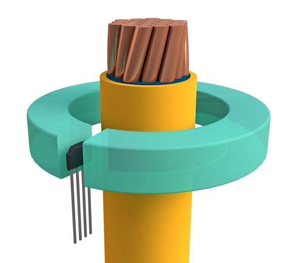
In a typical current sensing application, the sensor
Very short response time (2µs) is used in combination with a ring shaped soft
High linearity down to ±0.2% full scale ferromagnetic core. This core is recommended to
be laminated for high bandwidth applications. The
Very low thermal drift
MLX91217 is placed in a small air gap and the
Offset drift (MLX91217
High Speed High Accuracy Conventional Hall Current Sensor IC with Diagnostics
Datasheet
Contents
1. Features and Benefits ................................................................
................................................................................................
............................................................................................
............................................................ 1
2. Application Examples................................................................
................................................................................................
.............................................................................................
............................................................. 1
3. Description ................................................................
................................................................................................
................................................................................................
............................................................................
............................................ 1
4. Ordering Information ................................................................
................................................................................................
............................................................................................
............................................................ 3
5. Functional Diagram ................................................................
................................................................................................
...............................................................................................
............................................................... 4
6. Glossary of Terms ................................................................
................................................................................................
................................................................................................
..................................................................
.................................. 4
7. Pin Definitions and Descriptions ................................................................
................................................................................................
............................................................................
............................................ 4
8. Absolute Maximum Ratings ................................................................
................................................................................................
...................................................................................
................................................... 5
9. General Electrical Specifications ................................................................
................................................................................................
............................................................................
............................................ 6
10. Magnetic specification................................................................
................................................................................................
.........................................................................................
......................................................... 7
11. Analog output specification ................................................................
................................................................................................
.................................................................................
................................................. 7
11.1. Accuracy specifications .................................................................................................................... 7
11.2. Timing specifications ........................................................................................................................ 8
12. Self-
Self-diagnostic ................................................................
................................................................................................
................................................................................................
.....................................................................
..................................... 8
13. Recommended Application
Application Diagram ................................................................
................................................................................................
...................................................................
................................... 9
14. Recommended Application Diagram ................................................................
................................................................................................
.................................................................
................................. 10
15. Standard Information ................................................................
................................................................................................
........................................................................................
........................................................ 11
16. ESD Precautions................................................................
................................................................................................
................................................................................................
.................................................................
................................. 11
17. Packaging information ................................................................
................................................................................................
.......................................................................................
....................................................... 12
17.1. VA Straight leg (0xx)........................................................................................................................ 12
17.2. Trim and form type: SMD style TFT4K1 (1xx) ................................................................................ 13
17.3. Trim and form type: 90° 2x2x91.3 Bending-STD2 (2xx) ................................................................ 14
17.4. Sensor active measurement direction........................................................................................... 14
18. Contact ................................................................
................................................................................................
................................................................................................
..............................................................................
.............................................. 15
19. Disclaimer ................................................................
................................................................................................
................................................................................................
..........................................................................
.......................................... 15
390109121703 Page 2 of 15
Rev.006 – Apr-2020MLX91217
High Speed High Accuracy Conventional Hall Current Sensor IC with Diagnostics
Datasheet
4. Ordering Information
Product Temperature Package Option Code Packing Form Typical Sensitivity
MLX91217 L VA ACA – 000 BU/CR 10mV/mT (prog: 5..150mV/mT)
MLX91217 L VA ACA – 001 BU/CR 15 mV/mT (prog: 5..150mV/mT)
1
MLX91217 L VA ACA – 002 BU/CR 17 mV/mT (prog: 5..150mV/mT)
MLX91217 L VA ACA – 003 BU/CR 9 mV/mT (prog: 5..150mV/mT)
MLX91217 L VA ACA – 005 BU/CR 13 mV/mT (prog: 5..150mV/mT)
Table 1: Available ordering codes.
Legend:
Temperature
L from -40°C to 150°C ambient temperature
Code:
Package
VA SIP4-VA package, refer to Chapter 17 for detailed drawings
Code:
Option Code: ACA-x00 for sensitivity 10mV/mT; (programmable range: 5 to 150mV/mT)
ACA-x01 for sensitivity 15mV/mT; (programmable range: 5 to 150mV/mT)
1
ACA-x02 for sensitivity 17mV/mT; (programmable range: 5 to 150mV/mT)
ACA-x03 for sensitivity 9mV/mT; (programmable range: 5 to 150mV/mT)
ACA-x05 for sensitivity 13mV/mT; (programmable range: 5 to 150mV/mT)
ACA-0xx for Trim and Form shape: Straight leg/leads (see chapter 17)
ACA-1xx for Trim and Form shape: SMD style TFT4K1 (see chapter 17)
ACA-2xx for Trim and Form shape: 90deg 2x2x91.3 Bending-STD2 (see chapter 17)
Packing Form: BU for Bulk,
CR for Carton Reel - Radial taping
CA for Carton Reel - Ammopack
RE for Plastic Reel
Ordering “MLX91217LVA-ACA-005-CR”
Example: MLX91217 Conventional Hall current sensor in SIP4 VA package, temperature range -40°C to 150°C.
Sensitivity 13mV/mT. Parts delivered in Carton Reel (Radial Taping)
1
MLX91217-LVA-ACA-002 : customized sensitivity drift, VOQ = 1V
390109121703 Page 3 of 15
Rev.006 – Apr-2020MLX91217 High Speed High Accuracy Conventional Hall Current Sensor IC with Diagnostics Datasheet 5. Functional Diagram Figure 3: Block Diagram of the MLX91217: 6. Glossary of Terms Terms Definition TC Temperature Coefficient FS Full Scale, output referred. Corresponds to 2V excursion around 2.5V VOQ point T, mT Tesla, milliTesla = units for the magnetic flux density G Gauss = unit for the magnetic flux density [1mT = 10G] PTC Programming Through Connector IMC Integrated Magnetic Concentrator (IMC-Hall®) Table 2: Glossary of Terms 7. Pin Definitions and Descriptions Note: MLX91217 is pin-to-pin compatible with MLX91209. Pin # Name Type Description 1 VDD Supply Supply Voltage MLX91217 2 OUT Analog Current Sensor Output 3 TEST Digital Test and Factory Calibration 4 GND Ground Supply Voltage Table 3: Pin definitions and descriptions For optimal EMC results, it is recommended to connect the TEST pin to the Ground (see section 13). 390109121703 Page 4 of 15 Rev.006 – Apr-2020
MLX91217
High Speed High Accuracy Conventional Hall Current Sensor IC with Diagnostics
Datasheet

8. Absolute Maximum Ratings
Parameter                                              Symbol      Value       Unit

Positive Supply Voltage (overvoltage)                   VDD         +10         V

Reverse Voltage Protection                              VSREV       -0.3        V

Positive Output Voltage                                 VOUT        +10         V

Output Current                                          IOUT        ±70        mA

Reverse Output Voltage                                  VOREV       -0.3        V

Reverse Output Current                                  IOREV       -50        mA

Operating Ambient Temperature Range                      TA      -40 to +150    °C

Maximum Junction Temperature                            Tj,max   -55 to +155    °C

Package Thermal Resistance
(junction-to-ambient) θja is defined according JEDEC     θja        205         °C
1s0p board

Storage Temperature Range                                TS      -55 to +165    °C

Magnetic Flux Density                                   BMAX         ±3         T

ESD – Human Body Model                                 ESDHBM        2          kV

Table 4: Absolute maximum ratings

Exceeding the absolute maximum ratings may cause permanent damage. Exposure to absolute maximum-
rated conditions for extended periods of time may affect device reliability.

390109121703                                                                           Page 5 of 15
Rev.006 – Apr-2020
MLX91217
High Speed High Accuracy Conventional Hall Current Sensor IC with Diagnostics
Datasheet

9. General Electrical Specifications
Operating Parameters TA = -40 to 150°C, VDD = 5V±10%, unless otherwise specified.

Parameter                       Symbol     Test Conditions                            Min.     Typ.     Max.        Units
Nominal Supply Voltage            VDD                                                 4.5        5       5.5           V
                                           No OUT load
                                                            2
Supply Current                     IDD     LOW_POWER_MODE=0                                    12.5      15           mA
                                           LOW_POWER_MODE=1                                     10       13           mA
Output Impedance                  ROUT     Vout = 50% Vdd, RL = 6kΩ                              1           5         Ω
                                           OUT_MODE=0                                  1                 10           nF
Output Capacitive Load             CL
                                           OUT_MODE=1                                  10                47           nF
                                           Output resistive load for high linearity
Output Resistive Load              RL                                                  10       25      200           kΩ
                                           and diagnostic band.
Output Short Circuit                       Output shorted permanent to VDD.                  Not Destroyed
                                 ISHORT
Current                                    Output shorted permanent to GND.                  Not Destroyed
Linear Output Range              VOLIN     pull-down ≥ 10 kΩ                           10                90         %Vdd
                                           RL ≥ 10kΩ, RL ≤ 200 kΩ, VDD =5V
                  3
Diagnostic Band                  DIAG      DIAG_LEVEL = 0                              0                 4          %Vdd
                                           DIAG_LEVEL = 1                              96               100         %Vdd
                           3
BrokenGND Output Level                     RL ≥ 10kΩ, VDD = 5V                         96               100         %Vdd
                           3
BrokenVDD Output Level                     RL ≥ 10kΩ, VDD = 5V                         0                     4      %Vdd

                           3
                                VDD_UVD    Detected Voltage (Low to High)             4.0                4.5           V
Under-voltage detection
                                VDD_UVH    Hysteresis                                 0.01               0.2           V

                           3
                                VDD_OVD1   Detected Voltage (Low to High)             6.7                7.4           V
Over-voltage detection 1
                                VDD_OVH1   Hysteresis                                 0.37              0.66           V

                           3
                                VDD_OVD2   Detected Voltage (Low to High)             8.3                9.5           V
Over-voltage detection 2
                                VDD_OVH2   Hysteresis                                 0.2                0.8           V
                               Clamp_lo0 CLAMP_LEVEL=0                                 5         6           7      %Vdd
                               Clamp_hi0 CLAMP_LEVEL=0                                 92       93       94         %Vdd
                               Clamp_lo1 CLAMP_LEVEL=1                                 5         6           7      %Vdd
Clamped Output Level           Clamp_hi1 CLAMP_LEVEL=1                                 93       94       95         %Vdd
                               Clamp_lo2 CLAMP_LEVEL=2                                 7         8           9      %Vdd
                               Clamp_hi2 CLAMP_LEVEL=2                                 91       92       93         %Vdd
                               Clamp_lo3 CLAMP_LEVEL=3                                 9        10       11         %Vdd
                               Clamp_hi3 CLAMP_LEVEL=3                                 89       90       91         %Vdd

Table 5: General electrical parameters

2
    Default Factory Calibration
3
    Please refer to section 12 for more information on self-diagnostic modes.

390109121703                                                                                                     Page 6 of 15
Rev.006 – Apr-2020
MLX91217
High Speed High Accuracy Conventional Hall Current Sensor IC with Diagnostics
Datasheet
10. Magnetic specification
Operating Parameters TA = -40 to 150°C, VDD = 5V±10%, unless otherwise specified.
Parameter Symbol Test Conditions Min Typ Max Units
Operational Magnetic Field Range BOP ±15 ±130 ±450 mT
VOUT in [10%VDD, 90%VDD],
TA = 25°C
Linearity Error NL ±0.4 %FS
LOW_POWER_MODE=0
±0.2 %FS
LOW_POWER_MODE=1
Programmable Sensitivity S 5 15 150 mV/mT
Sensitivity programming Resolution SRES B = BOP 0.1 %
Table 6: Magnetic specification
11. Analog output specification
11.1. Accuracy specifications
Operating Parameters TA = -40 to 150°C, VDD = 5V±10%, unless otherwise specified.
Parameter Symbol Test Conditions Min Typ Max Units
T TA = -40 to 125°C ±5 mV
Thermal Offset Drift Δ VOQ
TA = -40 to 150°C ±8 mV
4 T TA = -40 to 125°C ±1.0 %S
Thermal Sensitivity Drift ΔS
TA = -40 to 150°C ±1.2 %S
Values for 50mV/mT sensitivity
Scales with typical sensitivity of Table 1
10 mVRMS
NOISE_FILTER=0
RMS Output Noise NRMS 7 mVRMS
NOISE_FILTER=1
5 mVRMS
NOISE_FILTER=2
3 mVRMS
NOISE_FILTER=3
VDD = 5V±5%, (for all option codes)
R
VOQ Ratiometry Δ VOQ VOQ = 20%VDD MLX91217LVA-ACA-002) ±0.4 %VOQ
VOQ = 50%VDD – (all other option codes) ±0.4 %VOQ
R
Sensitivity Ratiometry Δ S VDD = 5V±5%, B = BOP ±0.4 %S
Clamped output accuracy CLACC ±1 %Vdd
Table 6: Accuracy specifications – analog parameters
The accuracy specifications are defined for the factory calibrated sensitivity. The achievable accuracy is
dependent on the user’s end-of-line calibration. Resolution for offset and offset drift calibration is better
4
Except MLX91217-LVA-ACA-002
390109121703 Page 7 of 15
Rev.006 – Apr-2020MLX91217
High Speed High Accuracy Conventional Hall Current Sensor IC with Diagnostics
Datasheet
than 0.02%VDD. Trimming capability is higher than measurement accuracy. End-user calibration can
therefore increase the accuracy of the system.
11.2. Timing specifications
Operating Parameters TA = -40 to 150°C, Vdd = 5V±10%, unless otherwise specified.
Parameter Symbol Test Conditions Min Typ Max Units
Refresh rate Trr 0.8 1 2 μs
CL=10nF
NOISE_FILTER=0, LOW_POWER_MODE=0 2 3 μs
NOISE_FILTER=0, LOW_POWER_MODE=1 3 4 μs
NOISE_FILTER=1, LOW_POWER_MODE=0 3 4 μs
Step Response Time TR NOISE_FILTER=1, LOW_POWER_MODE=1 5 6 μs
NOISE_FILTER=2, LOW_POWER_MODE=0 4 5 μs
NOISE_FILTER=2, LOW_POWER_MODE=1 6 7 μs
NOISE_FILTER=3, LOW_POWER_MODE=0 8 9 μs
NOISE_FILTER=3, LOW_POWER_MODE=1 10 11 μs
Power on Delay TPOD Vout =100% of F.S. 1 ms
Ratiometry Cut-off
FRAT 250 Hz
Frequency
Table 7: Timing specifications of the high-speed analog output
12. Self-diagnostic
MLX91217 provides several self-diagnostic features, which prevent the IC from providing erroneous output signal in case of
internal or external failure modes.
Error Effect on Output Remarks
DIAG_LEVEL=0 active pull-down to GND
Calibration data CRC Error at power up and in normal mode
DIAG_LEVEL=1 active pull-up to VDD
Power-On Delay Pull-down to GND 1ms max followed by settling
Over-voltage Mode 1 Active pull-down to GND
DIAG_LEVEL=0 active pull-down to GND
Over-voltage Mode 2
DIAG_LEVEL=1 active pull-up to VDD
DIAG_LEVEL=0 active pull-down to GND Valid with enabled ratiometry
Under-voltage Mode
DIAG_LEVEL=1 active pull-up to VDD (Default: RATIOEN = 1)
Broken OUT Active pull-down to GND
Broken GND Output pulled up to VDD IC is switched off
Broken VDD Output pulled down to GND IC is switched off
Table 8: Description of the self-diagnostic modes in MLX91217
390109121703 Page 8 of 15
Rev.006 – Apr-2020MLX91217
High Speed High Accuracy Conventional Hall Current Sensor IC with Diagnostics
Datasheet
13. Recommended Application Diagram
Customers can re-program the parameters described in the table below by using the PTC-04 hardware and
the Product Specific Functions (PSF) libraries provided by Melexis. We recommend using the latest version of
the PSF and the firmware, with a communication speed of 10kbps (maximum output capacitor of 47nF).
Please contact your sales representative to get access to Melexis SoftDist platform and download the latest
software.
Parameter Bits Factory Setting Function
ROUGHGAIN 3 Trimmed Rough gain trimming
FINEGAIN 10 Trimmed Fine gain trimming
VOQ 12 Trimmed Offset trimming
OUT_MODE 1 0 0: low capacitive load (see section 14)
1: high capacitive load (see section 14)
DIAG_LEVEL 1 0 0: in diagnostic, output is pulled down to GND
1: in diagnostic, output is pulled up to Vdd
LOW_POWER_MODE 1 0 0: normal mode
1: low power mode with slower response time
CLAMP_LEVEL 2 1 Select clamping level (%VDD)
0: 6%/93%,
1: 6%/94%,
2: 8%/92%,
3: 10%/90%
NOISE FILTER 2 0/15 0: Noise filter: deactivated
1: Noise filter: 120kHz
2: Noise filter: 60kHz
3: Noise filter: 15kHz
CSTID 17 N/A Customer ID
5
The Noise Filter parameter is set to 1 for MLX91216LDC-ACV-002 IC version. The Noise Filter is deactivated for all
other option codes.
390109121703 Page 9 of 15
Rev.006 – Apr-2020MLX91217
High Speed High Accuracy Conventional Hall Current Sensor IC with Diagnostics
Datasheet
14. Recommended Application Diagram
Figure 4: Application Diagram with external Pull-Down resistance
Part Description Value Unit
C1 Supply capacitor, EMI, ESD 100 nF
Decoupling, EMI, ESD, OUT_MODE=0 1-10 nF
C2
Decoupling, EMI, ESD, OUT_MODE=1 8-47 nF
R1 Pull down resistor 10-200 kΩ
Table 7: Resistor and capacitor values
390109121703 Page 10 of 15
Rev.006 – Apr-2020MLX91217
High Speed High Accuracy Conventional Hall Current Sensor IC with Diagnostics
Datasheet
15. Standard Information
Our products are classified and qualified regarding soldering technology, solderability and moisture
sensitivity level according to standards in place in Semiconductor industry.
Reflow Soldering SMD’s (Surface Mount Devices)
• IPC/JEDEC J-STD-020
Moisture/Reflow Sensitivity Classification for Nonhermetic Solid State Surface Mount Devices
(classification reflow profiles according to table 5-2)
• EIA/JEDEC JESD22-A113
Preconditioning of Nonhermetic Surface Mount Devices Prior to Reliability Testing
(reflow profiles according to table 2)
Wave Soldering SMD’s (Surface Mount Devices) and THD’s (Through Hole Devices)
• EN60749-20
Resistance of plastic- encapsulated SMD’s to combined effect of moisture and soldering heat
• EIA/JEDEC JESD22-B106 and EN60749-15
Resistance to soldering temperature for through-hole mounted devices
Iron Soldering THD’s (Through Hole Devices)
• EN60749-15
Resistance to soldering temperature for through-hole mounted devices
Solderability SMD’s (Surface Mount Devices) and THD’s (Through Hole Devices)
• EIA/JEDEC JESD22-B102 and EN60749-21
Solderability
For further details about test method references and for compliance verification of selected soldering
method for product integration, Melexis recommends reviewing on our web site the General
Guidelines soldering recommendation. For all soldering technologies deviating from the one mentioned in
above document (regarding peak temperature, temperature gradient, temperature profile etc), additional
classification and qualification tests have to be agreed upon with Melexis.
For package technology embedding trim and form post-delivery capability, Melexis recommends to consult
the dedicated trim&form recommendation application note: lead trimming and forming recommendations.
Melexis is contributing to global environmental conservation by promoting lead free solutions. For more
information on qualifications of RoHS compliant products (RoHS = European directive on the Restriction Of
the use of certain Hazardous Substances) please visit the quality page on our
website: http://www.melexis.com/en/quality-environment
16. ESD Precautions
Electronic semiconductor products are sensitive to Electro Static Discharge (ESD).
Always observe Electro Static Discharge control procedures whenever handling semiconductor products.
390109121703 Page 11 of 15
Rev.006 – Apr-2020MLX91217
High Speed High Accuracy Conventional Hall Current Sensor IC with Diagnostics
Datasheet
17. Packaging information
17.1. VA Straight leg (0xx)
Package marking Hall plate position
2.105 ± 0.150 mm
FRONT SIDE BACK SIDE
91217 xx
2.579 ± 0.150 mm
xxxxxx yyww
Line 1: Product ID Line 1: IC Revision
Line 2: Wafer lot number Line 2: Assembly date code
year = yy
week = ww
Figure 5. VA/SIP 4L (single in-line package) / 18mm lead length - Package Information
390109121703 Page 12 of 15
Rev.006 – Apr-2020MLX91217 High Speed High Accuracy Conventional Hall Current Sensor IC with Diagnostics Datasheet 17.2. Trim and form type: SMD style TFT4K1 (1xx) 390109121703 Page 13 of 15 Rev.006 – Apr-2020
MLX91217
High Speed High Accuracy Conventional Hall Current Sensor IC with Diagnostics
Datasheet

17.3. Trim
      Trim and form type: 90°
                          90° 2x2x91.3 Bending-
                                       Bending-STD2 (2xx)

17.4. Sensor active measurement direction

Figure 6. VA/SIP 4L Package. Sensor’s active measurement direction

390109121703                                                                    Page 14 of 15
Rev.006 – Apr-2020
MLX91217
High Speed High Accuracy Conventional Hall Current Sensor IC with Diagnostics
Datasheet
18. Contact
For the latest version of this document, go to our website at www.melexis.com.
For additional information, please contact our Direct Sales team and get help for your specific needs:
Europe, Africa Telephone: +32 13 67 04 95
Email : sales_europe@melexis.com
Americas Telephone: +1 603 223 2362
Email : sales_usa@melexis.com
Asia Email : sales_asia@melexis.com
19. Disclaimer
The content of this document is believed to be correct and accurate. However, the content of this document is furnished "as is" for informational use only
and no representation, nor warranty is provided by Melexis about its accuracy, nor about the results of its implementation. Melexis assumes no responsibility
or liability for any errors or inaccuracies that may appear in this document. Customer will follow the practices contained in this document under its sole
responsibility. This documentation is in fact provided without warranty, term, or condition of any kind, either implied or expressed, including but not
limited to warranties of merchantability, satisfactory quality, non-infringement, and fitness for purpose. Melexis, its employees and agents and its affiliates'
and their employees and agents will not be responsible for any loss, however arising, from the use of, or reliance on this document. Notwithstanding the
foregoing, contractual obligations expressly undertaken in writing by Melexis prevail over this disclaimer.
This document is subject to change without notice, and should not be construed as a commitment by Melexis. Therefore, before placing orders or prior to
designing the product into a system, users or any third party should obtain the latest version of the relevant information.
Users or any third party must determine the suitability of the product described in this document for its application, including the level of reliability required
and determine whether it is fit for a particular purpose.
This document as well as the product here described may be subject to export control regulations. Be aware that export might require a prior authorization
from competent authorities. The product is not designed, authorized or warranted to be suitable in applications requiring extended temperature range
and/or unusual environmental requirements. High reliability applications, such as medical life-support or life-sustaining equipment or avionics application
are specifically excluded by Melexis. The product may not be used for the following applications subject to export control regulations: the development,
production, processing, operation, maintenance, storage, recognition or proliferation of:
1. chemical, biological or nuclear weapons, or for the development, production, maintenance or storage of missiles for such weapons;
2. civil firearms, including spare parts or ammunition for such arms;
3. defense related products, or other material for military use or for law enforcement;
4. any applications that, alone or in combination with other goods, substances or organisms could cause serious harm to persons or goods and that can be
used as a means of violence in an armed conflict or any similar violent situation.
No license nor any other right or interest is granted to any of Melexis' or third party's intellectual property rights.
If this document is marked “restricted” or with similar words, or if in any case the content of this document is to be reasonably understood as being
confidential, the recipient of this document shall not communicate, nor disclose to any third party, any part of the document without Melexis’ express
written consent. The recipient shall take all necessary measures to apply and preserve the confidential character of the document. In particular, the recipient
shall (i) hold document in confidence with at least the same degree of care by which it maintains the confidentiality of its own proprietary and confidential
information, but no less than reasonable care; (ii) restrict the disclosure of the document solely to its employees, agents, professional advisors and
contractors for the purpose for which this document was received, on a strictly need to know basis and providing that such persons to whom the document is
disclosed are bound by confidentiality terms substantially similar to those in this disclaimer; (iii) use the document only in connection with the purpose for
which this document was received, and reproduce document only to the extent necessary for such purposes; (iv) not use the document for commercial
purposes or to the detriment of Melexis or its customers. The confidentiality obligations set forth in this disclaimer will have indefinite duration and in any
case they will be effective for no less than 10 years from the receipt of this document.
This disclaimer will be governed by and construed in accordance with Belgian law and any disputes relating to this disclaimer will be subject to the exclusive
jurisdiction of the courts of Brussels, Belgium.
The invalidity or ineffectiveness of any of the provisions of this disclaimer does not affect the validity or effectiveness of the other provisions.
The previous versions of this document are repealed.
Melexis © - No part of this document may be reproduced without the prior written consent of Melexis. (2020)
IATF 16949 and ISO 14001 Certified
390109121703 Page 15 of 15
Rev.006 – Apr-2020You can also read