Nanoelectronics Miniaturisation in Electronics: Scaling Challenges
←
→
Page content transcription
If your browser does not render page correctly, please read the page content below
Nanoelectronics
                Miniaturisation in Electronics:
                      Scaling Challenges

    With slides from:
    Prog. Aidan Quinn (Nanotechnology Group, Tyndall)
    Prof Jean-Pierre
    Prof. Jean Pierre Colinge (formerly
                               (formerl head of MNE Centre
                                                     Centre, T
                                                             Tyndall)
                                                               ndall)
    Dr Lida Ansari (Electronics Theory Group, Tyndall)
    Dr Vladimir Djara (ex - Silicon Research Group & CFF, Tyndall)
    Dr Barry O’Sullivan (ex – SRG, Tyndall)
1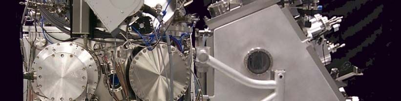
CMOS Scaling

• Microprocessor performance: 2011 vs 1971
• Semiconductor Industry Overview (ITRS)
    • IInternational
               i   lTTechnology
                        h l      R
                                 Roadmap
                                     d     ffor SSemiconductors
                                                     i  d       (2011 Edi
                                                                      Edition)
                                                                           i )
         http://www.itrs.net/Links/2011ITRS/Home2011.htm (pub. Feb. 2012)
         Executive Summary,y, Lithography,
                                   g p y, Emerging g g Research Devices,, Emerging
                                                                              g g
         Research Materials sections

• Moore’s Law (Scaling).
              (      g)

• Silicon Process Scaling Challenges.
    –   Lithography
    –   Transistor
    –   Gate Dielectric
    –   Interconnects
    –   Power Dissipation
2
First Transistor (1947)

                    Transistor
              “Transforming resistor”

          At Bell laboratories in 1947

3
Discrete Electronic Circuits
Electronic elements wired or
soldered together
g onto circuit
boards.
Large space
Expensive
4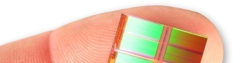
Early Integrated Circuits

                                         Robret Noyce: First
            Nobel Prize, 2000         monolitic integrated circuit

Jack Kilby: Inventor of
the first integrated circuit
– at Texas Instruments in
1959

5                                       Only 4 transistors!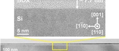
Intel Quad‐Core (2,000,000,000 transistors), 2008
One centimetre
The first transistor 1947
High speed of microprocessors
Higher numbers of Low cost
transistors on a chip
4000 transistors of 22 nm L
Low power consumption
i
gate length fit across the
width of a human hair!
6
Past & Present:
                            Silicon Microprocessors
                                         p          at the 20 nm length
                                                                    g scale
                            (a human hair is about 50,000 nm in diameter)

 1971:                                         2011:
 Intel 4004. First commercially                8 x 128 Gbit die
 available microprocessor:
 5 kilobits of data (~ a text message)         1TTerabit
                                                     bit off d
                                                             data
                                                               t ((~50,000
                                                                    50 000 photos
                                                                            h t
 ~600 kHz clock frequency                      from a 3 Megapixel camera)
                                               ~3 GHz clock frequency
                                                                  q    y

7 Source: Intel (6/12/11)
Near Future: 3D Nanotransistors
Lg
Drain
Gate
W
Source
Tsi
A-A’
200 nm
BOX
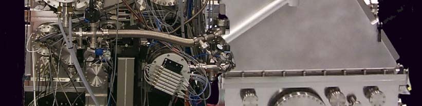
Nanoscale Tri-gate Transistors Fabricated at Tyndall
using Electron-Beam
Electron Beam Lithography (Prof. J.P. Colinge).
Electron microscopy images from Intel Ireland (2014).
8Classical CMOS Field-effect Transistor
Gate Oxide gate
source SiO2 VG drain
VS VD
n+ n+
L
type silicon
p-type
p
• First MOSFET IC’s produced in 1963
• SiO2 was the gate dielectric of choice until 2008
• Channel / g
gate oxide interface critical to device p
performance
and long-term stability
• L is the channel (gate) length
9 Source: Barry O’SullivanIntroduction
What is a MOSFET ?
MOSFET: Metal Oxide Semiconductor Field Effect Transistor
CMOS Inverter
Vin Vout
45-nm node
(INTEL)
10
10MOSFETs are Everywhere
MOSFET: Metal Oxide Semiconductor Field Effect Transistor
Data centres
11
11Transistor is a switch!
Julius Edgar Lilienfeld ,
1925
Dawon Kahng, 1959
Gate
Source Drain
12MOS Gate Stack
→ Ideal Case
M
Source O Drain
S
13
13Introduction
MOS Gate Stack
→ Ideal Case
M O S
C d ti B
Conduction Band
d
Fermi Level
S
Source D i
Drain
Valence Band
Energy
gy
Distance
14
14Introduction
MOS Gate Stack
→ Ideal Case
V < VT
M
Source O Drain
S
OFF state
15
15Introduction
MOS Gate Stack
→ Ideal Case
V < VT
M
Source O Drain
S
OFF state
16
16Introduction
MOS Gate Stack
→ Ideal Case
V < VT
M
Source O Drain
S
OFF state
17
17Introduction
MOS Gate Stack
→ Ideal Case
V < VT
M
Source O Drain
S
OFF state
18
18Introduction
MOS Gate Stack
→ Ideal Case
V = VTh
M
Source O Drain
S
Threshold
Threshold
19
19Introduction
MOS Gate Stack
→ Ideal Case
V > VTh Qinv = Cox . (V ‐ VTh)
M
Source O Drain
S
ON state
20
20Introduction
MOS Gate Stack
→ Non‐ideal Case
V > VTh Qinv + Qtrap = Cox . (V
( + ΔV ‐ VTh)
M
Source O Drain
S
Qtrap
21
21Introduction
MOS Gate Stack
→ Non‐ideal Case
V > VT Qinv + Qtrap = Cox . (V
( + ΔV ‐ VT)
M
Source O Drain
S
Qtrap
22
ΔV yields degradation of SS 22Motivation
Number of transistors in ICs had doubled every year from
the invention of the IC in 1958 until 1965 and predicted
that the trend would continue “for at least ten years”
Gordon Moore
Traditional
d l scaling
l
increasingly challenging
new materials & novel
devices
Source ITRS
23Moore’s Law: Number of transistors per unit
area doubles everyy 2 yyears
Source: Intel (Oct. 2009)
24Top-down MOS transistors 25
Typical feature size for a given ITRS node/year

Definitions of typical feature size for a given ITRS node/year
NB Some features are even smaller
                             smaller, e
                                      e.g.
                                         g gate length

     Source ITRS 2011
26
Gate Pitch (Intel)
Source: Intel (Oct. 2009)
27Static Random Access Memory (SRAM) Cell Size
Source: Intel (Oct. 2009)
28Scaling Nodes (term gradually being replaced by “Year
of First Production” due to differences in scaling rates)
Why: 500 nm, 350 nm, 250 nm, 180 nm, 130 nm, 90 nm, 65 nm, 45 nm, 32 nm ?
Ln Ln+1
Ln
Area of 1 transistor: An+1 = An / 2 An+2 = An+1 / 2
An = Ln2 = Ln+12 = An / 4
= Ln+22
Ln+12 = Ln2 /2 Ln+22 = Ln2 /4
Ln+1 = Ln /2 Ln+2 = Ln /2
2 1.4 1/2 0.7
29Moore’s Law driven by scaling
1000 0.5m
All leading-edge logic products:
e size ((nm)
0.35m
Technology Node
0.25m = 2x transistor
0 18
0.18m density of previous
0.13m node
0.2m 90nm
100 130nm
65nm
45nm
eature
Transistor 70nm 30nm
50nm
Physical Gate
30nm
Fe
Length 20nm 15nm
10
1990 1995 2000 2005 2010
Year
Source ITRS 2001
30Moore’s Law driven by scaling
All leading-edge logic products:
10000
gy node ((nm)
1000
100
Technolog
10
T
1
1970 1980 1990 2000 2010 2020 2030
year
y
31 Source: ITRS 2015Top-down MOS transistors 32 J. Maiz, Intel, 2007
Top-down MOS transistors

                                              14 nm
                                              2014

     Intel, 2011
33
Top-down MOS transistors
Intel, 2010
34Predicted Feature Sizes in CMOS
NB: Sizes are predicted,
manufacturing solutions have not been identified/optimised for all nodes.
Source ITRS ’11, Executive Summary
35Predicted Feature Sizes in CMOS
NB: Sizes are predicted,
manufacturing solutions have not been identified/optimised for all nodes.
36 Source ITRS ’11, Executive SummaryLithography Challenges (Near Term)
Source: ITRS ’11, Lithography Section
37 http://www.itrs2.net/itrs-reports.htmlLithography Challenges (Near Term)
YEAR OF PRODUCTION 2015 2017 2019 2021 2024 2027 2030
Logic device technology naming P70M56 P48M36 P42M24 P32M20 P24M12G1 P24M12G2 P24M12G3
Logic industry "Node Range" Labeling (nm) "16/14" "11/10" "8/7" "6/5" "4/3" "3/2.5" "2/1.5"
finFET
finFET finFET finFET
Logic device structure options LGAA VGAA, M3D VGAA, M3D VGAA, M3D
FDSOI FDSOI LGAA
VGAA
DRAM
DRAM minimum ½ pitch (nm) 24 22 18.0 15.0 12.0 9.2 7.7
CD control (3 sigma) (nm) [B] 24
2.4 22
2.2 18
1.8 15
1.5 12
1.2 09
0.9 08
0.8
Mininum contact/via after etch (nm) [H] 24 22 18 15 12.0 9.2 7.7
Minimum contact/via pitch(nm)[H] 72 66 54 45 36 28 23
Overlay (3 sigma) (nm) [A] 4.8 4.4 3.6 3.0 2.4 1.8 1.5
Flash
2D Flash ½ pitch (nm) (un‐contacted poly) 15 14 12 12 12 12 12
Flash 3D Layer half‐pitch targets (nm) 80.0 80.0 80.0 80.0 80.0 80.0 80.0
3D NAND minimum metal pitch(nm) 20.0 20.0 20.0 20.0 20.0 20.0 20.0
CD control (3 sigma) (nm) [B] 1.5 1.4 1.2 1.2 1.2 1.2 1.2
Overlay (3 sigma) (nm) [A] 5.1 4.7 3.9 3.9 3.9 3.9 3.9
MPU / Logic
MPU/ASIC Minimum
Mi i M
Metall ½ pitch
i h ((nm)) 26 18 12 10 60
6.0 60
6.0 60
6.0
MPU/ASIC finFET fin minimum 1/2 pitch (nm) 21 18 12
Lateral Gate All Around (LGAA) 1/2 pitch 12 10
Vertical Gate All Around (VGAA) 1/2 pitch 10 6.0 6.0 6.0
Contacted poly half pitch (nm) 35 24 21 16
Physical Gate Length for HP Logic (nm) 24 18 14 10
Vertical Gate All Around (VGAA) pitch (nm) 20 12 12 12
Gate CD control (3 sigma) (nm) [B] 2.4 1.8 1.4 1.0
Metal CD control (3 sigma) (nm) [B] 2.6 1.8 1.2 1.0 0.6 0.6 0.6
Fin CD control (3 sigma) (nm) [B] 0.40 0.30 0.30
FIN or LGAA LER [C] 0.40 0.30 0.30
Gate LER [C] 2.4 1.8 1.4 1.0
Metal LWR [C] 3.9 2.7 1.8 1.5 0.9 0.9 0.9
Source: ITRS 2.0, 2015, Lithography Section,
38 http://www.itrs2.net/itrs-reports.htmlMarket estimations
Players: Intel, Samsung, TSMC,.....
g in strategy
Changes gy ahead: optimizing
p gpperformance at each node p
prior to lauch next one
39 http://spectrum.ieee.org/semiconductors/devices/intel-finds-moores-laws-next-step-at-10-nanometersLithography (Optical)
1.A laser beam writes the circuit pattern for a
microchipp on a layer
y of light-sensitive
g polymer
p y
(photoresist) that rests atop a layer of
chromium on a transparent substrate (e.g.
quartz). The sections of polymer struck by the
beam can be selectively removed (developed).
(developed)
2.The exposed sections of chromium are
removed by etching, and the rest of the
polymer is then dissolved.
dissolved The result is a
mask—the equivalent of a photographic
negative.
3.When
3 When a beam of monochromatic ultraviolet
light is directed at the mask, the light passes
through the gaps in the chromium. A lens
shrinks the p pattern by
y focusing
g the light
g onto a
layer of photoresist on a silicon wafer.
4.The exposed parts of the photoresist are
removed, allowing the replication of the
pattern in miniature on the silicon chips using
etching, metal deposition, ion implantation etc.
Scientific American, 2001
40Optical Lithography
UV Light
Chrome Scientific American, 2001
41Optical Lithography 42
Lithography (e-beam)

43
Optical Lithography:
     Wavelengths and Sources (NB Historical)

                            deep ultraviolet (DUV)

                                      Immersion Lithography
                                       & Multiple Patterning

                                        → Abandoned

     Extreme ultraviolet (EUV)
                                             → 2017-20 ?

44
Material Challenges in Lithography
• 157nm Wavelength (never used)
– Photoresist
– Quartz is no longer transparent at 157 nm - WHY (homework)
– CaF2 is the likely replacement material for quartz lens
– Transparent mask pellicles (degradation)
– Current materials fail at doses of ~10 J/cm2
– Goal is >1000 J/cm2
45Challenges in Lithography
• 13nm ((EUV)) Wavelength
g ((cf. ITRS 2011 Litho Section))
– Source power, source lifetime
– Lens and mask reflective instead of refractive
– Reflective surface is multiple alternating thin layers of Mo:Si
– Mask defects
– Suitable photoresist for EUV (sulfone terpolymers, truxene derivative)
46 SEM image in 22nm line patternEUV: Reflective Optics
EUV Mask (UC Berkeley)
47EUV Lithography: 13nm
Mask
EUV Stepper Prototype 120 mm x 104 mm field size 50nm Lines Printed
with EUV Lithography
All Optical Elements Must Reflect 13nm Radiation
Source: Intel
48Source: Intel 49
Lithography Technology (ITRS 2011 Lithography Chapter)

50
E-beam lithography

51
E-beam lithography

Down to 10 nm
resolution
    l ti

52
Moore’s Law driven by scaling
All leading-edge logic products:
10000
gy node ((nm)
1000
100
Technolog
10
T
1
1970 1980 1990 2000 2010 2020 2030
year
y
53 Source: ITRS 2015Complementary Metal-oxide Semiconductor (CMOS)
Technology Roadmap
“Classical”
Classical CMOS: “the
the same only smaller (and faster)”
faster)
Non-classical CMOS
• SOI
SO (Silicon
Sl on Insulator)
l New Technologies
• Si/SiGe
• Quantum devices
• High-K dielectrics (2007)
• Spin-electronics
Feature sizes ~ 100 nm • Molecular electronics
Intel Fab 24, Leixlip
• Quantum Computing
2004 2006 2008 2010 2012 2014 2016 2018
sizes 10 nm
sizes~10
• Near term: Develop manufacturable non-classical or hybrid
alternatives to CMOS
• Longg term: Invention a feasible new information and signal
g
processing technology addressing “beyond CMOS” applications
54The future: Beside and Beyond Silicon
Taxonomy for Nanoscale Information Processing
Source: International Technology Roadmap for Semiconductors 2009
55Information Processing & Storage in the 21st
Century: Speed, Size, Cost, Power Consumption
Estimated Parameters for Emerging
g g Research Devices and Technologies
g in 2016
“Perfect”:
Perfect :
Small
Fast
Cheap
Low-Power
Source: ITRS 2005
56Why Scaling ? Constant field scaling (1960-2003). Theory predicts increased speed and lower power consumption of digital MOS circuits when the critical dimensions are scaled down. 57
Introduction
            Dynamic Power Dissipation
            → Scaling Supply Voltage (VDD)

     LOG(Idrain)

     ION                                     Silicon

     IOFF
                                                       Vgate
              0                        VDD
                                                               58
58
Introduction
Dynamic Power Dissipation
→ Scaling Supply Voltage (VDD)
LOG(Idrain)
III‐V (high mobility)
ION Silicon
IOFF
Vgate
0 VDD VDD
59 VDD = VGS at the current settled as “on” 59Introduction
Dynamic Power Dissipation
→ Scaling Supply Voltage (VDD)
LOG(Idrain)
III‐V (high mobility)
ION Silicon
1/slope = subthreshold swing = SS [mV/dec.]
IOFF
Vgate
0 VDD VDD
60
60Total Power Dissipation in CMOS Circuitry
Ptotall = Pdynamic
d + Pstatic
Leakage
Charging/discharging
load capacitance
61
61Introduction
Dynamic Power Dissipation
→ Scaling Supply Voltage (VDD)
Pdynamic = Cload . VDS2 . f
IDS = µ . Cox . ((w/L)) . ((VGS‐VTh) . VDS
L and w, length and width of the channel, Cox capacitance of insulating layer,
VGS , VTh and VDS voltage
g gate‐source
g , threshold (V
( DD) and drain‐source
Introduce high mobility materials to reduce VDS
Material Si Ge GaAs In0.53Ga0.47As InAs InSb
Electron Mobility
1400 3900 8500 14000 40000 78000
(cm2/Vs)
Hole mobilityy
450 1900 400 300 500 850
(cm2/Vs)
62
62The holy grail !
Monolithic integration
g of high‐k/III‐V
g / and high‐k/Ge
g / on Si
High electron mobility channel: III‐V High hole mobility channel: Ge
High k oxide
High‐k
63
63Strained Silicon
Heteroepitaxy
p y – e.g.
g Growth of SiGe on Si
1 1. Growth of SiGe on Si (4%
lattice mismatch)
2. Below a critical thickness –
strained growth
3
3. Ab
Above critical
i i l thickness
hi k -
dislocations
2 3
http://www.phy.cam.ac.uk/sige/content.php?pg=bg_strain
64Strained PMOS and NMOS devices
Compressive Strain Tensile Strain
Source: Intel (Oct. 2009)
65Strained PMOS and NMOS devices 66
Problems with ultra-thin SiO2 Gate Oxide layers

                       Gate Oxide        gate
             source       SiO2            VG               drain
               VS                                           VD

                  n+                                      n+
                                     L
                                                   yp silicon
                                                p-type
                                                p

     • At thickness 1 - 1.2 nm, excessive direct tunnelling in SiO2
         – Leakage currents in excess of 100 A cm-2
     • Boron penetration through SiO2 layer from polysilicon in p-
       channel MOSFET’s
               MOSFET’s, after high temperature processing
     • Degenerate doped polysilicon gate electrodes
         – In inversion
              inversion, polysilicon becomes depleted of carriers
       Source: Barry O’Sullivan (High-K group, Tyndall)
67
Gate oxide (dielectric)
Gate
1.2nm
12 SiO2
Silicon
substrate
• 90 nm process
• 1.2 nm gate oxide thickness = 5 atomic layers
• Current Leakage is a Serious Problem
Source: Intel
68Gate Leakage Currents 69
Solution: High-K () Gate Dielectric
C ε0
T
A T
C: Capacitance A: Area K (): Dielectric Constant
T: Thickness (physical)
Effective/Electrical Oxide (SiO2) Thickness (EOT) = T KSiO2 / K
• If material with higher permittivity is introduced, increase thickness
to get same capacitance per unit area
– As layer is physically thicker,
thicker reduced tunnelling currents
• Replace polysilicon electrodes with metal electrodes
– Can ensure adequate
q band offsets for both n and p
p-MOS devices
70Solution: High-K () Gate Dielectric
Effective/Electrical Oxide ((SiO2) Thickness ((EOT)) = T KSiO2 / K
71 http://www.tibercad.org/sample_application/article/multiscale_simulation_mosfets_based_high_k_oxidesStatic Power Dissipation
→ Controllingg Leakage
g
Oxide thickness scaling
tox
d gate lleakage
‐> increased k
Pstatic = Ileakage . VDD
Id = µ . Cox . (W/L) . (Vg‐VT) . Vds
Cox = ε0 . k / tox
Introduce high‐k materials to increase tox
72Source: Intel 73
hafnium silicate,
zirconium silicate,
 hafnium dioxide
zirconium dioxide
HfSiON

 J. Maiz,
I t l 2007
Intel,

 74
Requirements of a new dielectric: Material

     • Good stoichiometry (i
                          (i.e.
                             e no vacancies and/or other defects)

     • Structure (amorphous vs. crystalline)

     • Uniform continuous films; small roughness
     • Minimal thickness of interfacial layer(s)
     • Thermal stability with respect to silicon
         • Subsequent
                q     to annealing
                                 g at temperatures
                                         p         up
                                                    p to 1000oC

     • Low concentration of impurities (C, H, metals, etc.)

      Source: Barry O’Sullivan (High-K group, Tyndall)
75
Requirements of a new gate dielectric
Processing and Integration Issues
• Compatibility with polysilicon processing (or metal gates)
• Diffusion barriers to dopants
• No metal diffusion into the Si channel
• Manufacturability (tools, etc.)
• Stability in air / water solubility ?
Source: Barry O’Sullivan (High-K group, Tyndall)
76Requirements of a new dielectric : Electrical
• High dielectric constant (10 < < 50)
• Low leakage current density (< 1 A cm-2 at VGS = VDD)
• Equivalent oxide thickness (Teqq) less than 1.2 nm
• Large band gap (> 6 eV) / suitable band offsets (> 1 eV)
• Electron / hole mobility ~ 95% SiO2 / Si devices at 1 MV / cm
• Low concentration of bulk traps / fixed charge; no hysteresis
– Small VFB shifts (cf
(cf. ideal)
• Reliability comparable to SiO2
• Low interface state density, ~ mid 1010 cm-2 eV-1
Source: Barry O’Sullivan (High-K group, Tyndall)
77High‐k Materials
• Gate dielectric, silicon dioxide, is only a few
atomic layers thick now leakage current
increases, as
45 nm
Huff et. al., Microelectronic Engineering, 69 (2003)
[J. Appl. Phys., 73 (1993) & 15 (2000), 83 (1998)]
78Crafting Films with Atomic Layer Deposition
x y
B x
y
A x
A
Step 1 Step 3
B
A A
Step 2 Step 4
79Atomic Layer Deposition (ALD) of Al2O3 80
Current Gate Stack (based on HfO2 high-K)

81
High K Gate

     • Control Interface, Stress, Fixed charge, etc.
        – New additives?
     • New Chemical Precursors
     • New Gate Electrode Material
     • New Etch Chemistries
     • Future: Need K ~50-100

82
Interconnects 83 https://www.bit-tech.net/hardware/cpus/2010/06/10/how-to-make-a-cpu-from-sand-to-shelf/3
84 Source: K. Monnig, SEMATECH
Interconnect Material Challenges at 65 nm
                         node
                                                                  8 layers
                                                                      y of metal

         Low K carbon-doped oxide

     Copper
       pp interconnects                                        Device
      Two-layer dielectric for low capacitance and low cost.        J. Maiz, Intel, 2007
      Must Reduce Dielectric Constant (K) and Resistance
85
Interconnect Resistance: Barrier Layers
~ 20 nm barrier layer
120
erconnect
100
80 20nm Barrier
Cu % of Inte
60 10nm Barrier
40 1nm Barrier
20
0
180 130 90 65 45
Interconnect Size (nm)
• Need thin but effective barrier to prevent Cu diffusion
• Would prefer Self Assembling Precursors vs deposition
• Need Adhesion to all layers
• New material &/or deposition technology…
86Interconnect Resistance: Increased Resistivity
• Need thin but effective barrier to p
prevent Cu diffusion
• Would prefer Self Assembling Precursors vs deposition
• Need Adhesion to all layers
• New material &/or deposition technology…
87Low-K materials for high speed gates
SiO2 has a relative dielectric constant
K r 3.9
0
Low-k materials those that have dielectric constant
smaller than SiO2.
(i.e. K= 3.7 for SiCN, K= 3.0 for C:SiO2)
Dielectric constant influences in the capacitance of
the gate and thus, it may limit its response time
S K 0
C RC
88
dLow-K materials for high speed gates 89 Source: K. Monnig, SEMATECH
90
91 Source: K. Monnig, SEMATECH
Super Materials Needed for low-K

     •   Stress in process & assembly a big issue
     •   Design Electrical & Mechanical Properties
     •   Improve adhesion between materials
     •   Molecular self assembly…
     •   Nano-materials
         Nano  materials

92
Very Low-K: Porous Materials
Source: Intel
Low--k xerogel structure
Low
Mechanical Strength
S and Integration Issues
93Self Assembled Nanoporous Low K Dielectric
(M A Morris,
(M.A. Morris Chemistry Dept.,
Dept UCC)
94Power Dissipation – Key Challenge (old graphic)
Intel
95Silicon Scaling Summary
• Scaling continues …………….
• Lithography: New tools and processes needed
• Many new materials needed
– Lithography
– Transistor
– Interconnects
– Molecular assembly….
• Lower K ILDs are weaker
– Mechanical issues in processing
– Mechanical issues in assembly
96Dynamic Power Dissipation
→ Scaling Supply Voltage (VDD)
Pdynamic = Cload . VDD2 . f
Id = µ . Cox . (W/L) . (Vg‐VT) . Vds (@Vds = VDD)
Introduce high mobility materials to reduce VDD
Material Si Ge GaAs In0.53Ga0.47As InAs InSb
Electron Mobility
El M bili
1400 3900 8500 14000 40000 78000
(cm2/Vs)
Hole mobility
450 1900 400 300 500 850
(cm2/Vs)
97
97Introduction
Challenges for III‐V MOSFETs
Integration of Scaling Integration of
High‐k on III‐V (S/D Resistance) III‐V on Si
Aspect Ratio Trapping
HfO2//Al2O3//InGaAs “Nikelide”
Nikelide Phase
Waldron, ECST, 45:4, 115 (2012)
Oxland,, IEEE EDL,, 33:4,, 501 (2012)
( )
Chu, APL, 99:4, 042908 (2011)
Bonding
C t l off oxide/InGaAs
Control id /I G A TTargett ffor 12
12‐nm node:
d
interface ρC = 5 × 10‐9 Ω.cm2
Target:
Target
Yokoyama, IEEE EDL, 32:9, 1218 (2011)
SS ~ 60 mV/dec.
98
98Introduction
Challenges for III‐V MOSFETs
Integration of Scaling Integration of
High‐k on III‐V (S/D Resistance) III‐V on Si
Aspect Ratio Trapping
HfO2//Al2O3//InGaAs “Nikelide”
Nikelide Phase
Waldron, ECST, 45:4, 115 (2012)
Oxland,, IEEE EDL,, 33:4,, 501 (2012)
( )
Chu, APL, 99:4, 042908 (2011)
Bonding
C t l off oxide/InGaAs
Control id /I G A TTargett ffor 12
12‐nm node:
d
interface ρC = 5 × 10‐9 Ω.cm2
Target:
Target
Yokoyama, IEEE EDL, 32:9, 1218 (2011)
SS ~ 60 mV/dec.
99
99You can also read