ORGANIC AND PRINTED ELECTRONICS - components - Coating and converting
←
→
Page content transcription
If your browser does not render page correctly, please read the page content below

NO 28, SEPTEMBER 2019
                                              ORGANIC AND PRINTED ELECTRONICS

                                                          GR  E E N
                                                           IS S U E

components                         events
Work in progress                   Solving complex
RK Print Coat Instruments          manufacturing issues
                                   InPrint

                            including        news | www.ope-journal.com
International Exhibition of Print Technology
                                   for Industrial Manufacturing

  12 – 14 NOVEMBER 2019
  Munich Trade Fair Centre, Germany

Discover innovative technologies and smart solutions for printing on a
variety of materials and surfaces in different industry sectors.

• Printing Machinery & Systems               • Screen, Digital and Speciality Printing Inks
• Components & Print Heads                   • Pre-Press Devices, Processing & Finishing Equipment
• UV Technology, Drying & Curing Equipment   • Software Solutions

 Technical conferences on all three exhibition days
                                                                                     Organiser:

www.inprintmunich.com
EDITORIAL   3

                                   Martin Hirschmann
                                   Editor OPE journal
                                   Mail: martin.hirschmann@dfv.de

Dear Readers,
The biggest challenge of the 21st century will be the way we are dealing
with the impending climate crisis, whose effects can already be felt right
now. Applying sustainable or ‘green’ principles to production and the
world of business seems like an absolute necessity, when we consider
the dramatic consequences that climate change will have according to
an overwhelming number of scientists from many different disciplines.
The organic and printed electronics industry may only play a minor role
in the overall picture when we are looking at its volume – the amount
of waste it creates is almost negligible, and its production methods
are certainly not as energy-intensive as other industrial sectors. On the
other hand, our example can influence other sectors, and our products
can indeed make an enormous difference. I am not only thinking about
organic photovoltaics here (they will play a major role on the following
pages though). Sensors in packaging may avoid food losses, the aviation
sector will soon profit from lighter (and therefore fuel-saving) cabin
interiors thanks to printed electronics, and smart devices can help in
saving energy or making infrastructure more intelligent than today.
In any case, it makes sense to ‘embrace’ the major challenge of climate
change, instead of denying its existence, as some world leaders and
industry giants still try to do. There are enormous opportunities for
businesses and new products that make this world more sustainable.
And there are dedicated researchers, visionaries, and companies that
want to invest in this green future.
Best regards
Martin Hirschmann

                www.linkedin.com/company/ope-journal                @OPEjournal
4         EVENT DIARY

          2019

          ICFPE 2019
          (International Conference on                                                 Location: Taipei Nangang Exhibition Center Hall 1, Taiwan
                                                          23-25 October 2019
          Flexible and Printed Electronics)                                            Organiser: ICFPE
          https://expo.itri.org.tw/2019ICFPE

          IDTechEx Show! USA 2019                                                      Location: Santa Clara Convention Center, California, USA
          www.idtechex.com/                               20-21 November 2019
                                                                                       Organiser: IDTechEx
          printed-electronics-usa/show/en

          InPrint Munich 2019                             12-14 November 2019
                                                                                       Location: Munich Trade Fair Centre
          www.inprintmunich.com                                                        Organiser: MackBrooks Exhibition

          2020

                                                                                       Location: Munich Trade Fair Centre, Germany
                                                          24-26 March 2020             Organisers: Messe München, OE-A
                                                                                       www.lopec.com

          IDTechEx Show! Europe 2020                                                   Location: Estrel Berlin, Germany
          www.idtechex.com/                               13-14 May 2020
                                                                                       Organiser: IDTechEx
          printed-electronics-europe/show/en

    LabCo
    The Universal Genius for OPV and RFID
                                                                                                        KROENERT          The Coating Machinery Experts
    for roll-to-roll coating, printing and laminating

                                                                                                             Printed Electronics              Flexible Photo Voltaics

                                                                                                                     OLED Wall                       Flexible Display

    The perfect solution for laboratory, prototyping or production. With its modular
    design and versatility, the compact machine is ideal for the widest variety of applica-
    tions. The LabCo produces high-precision results which are to 100% transferable to
    wider working widths, also in clean room environments. The LabCo is available to
    our customers for testing at our in house Technology Center.
    Contact us now! www.kroenert.de                                                                          Flexible Solar Film                     Solar Enery Cell

                                                        See us on our                                                              www.kroenert.de
                                                        booth No. 4/B17
                                                                                                                   No 28 | September 2019 | OPE journal
CONTENTS   5

8    HIGHLIGHTS FROM OPE-JOURNAL.COM

     GREEN ISSUE
     8   The greenest energy choice
         Heliatek [Member of OE-A]

     11 Ultra-short pulse lasers –
        improving photovoltaic production
        Coherent

     15 Shedding light on the sustainable
        aspects of printed electronics
        OE-A

     18 The interface between
        photovoltaics and printed electronics
        VDMA / Oxford PV [Member of OE-A]

     20 Energy is the key
        Dracula Technologies [Member of OE-A]
18
     COMPONENTS
     22 Work in progress
        RK Print Coat Instruments

     EVENTS
     24 Guaranteed head start in information
        LOPEC 2020

     25 In the heart of Silicon Valley
        IDTechEx Show USA

26   26 Solving complex manufacturing issues
        InPrint

     MILDNER’S COLUMN
     28 How “Green” is Printed Electronics?

     BEYOND THE DESK
     29 A gentle alternative for health applications

     SUPPLIERS DIRECTORY

            NEWS
     3   EC Workshop on ‘Smart Bioelectronic and
         Wearable Systems’
     4   FINAL CALL! – Take part in the
29       OE-A Competition 2020 and globally
         promote your printed electronics
         product and vision
6 HIGHLIGHTS FROM OPE-JOURNAL.COM
Isorg and Sumitomo Chemical Neotech AMT and FAPS win TÜV
announce partnership to develop SÜD Innovation Award 2019
organic photodetectors
For the third time, TÜV SÜD's innovation prize honours success-
Isorg (Grenoble, France), a pioneer in organic photodetectors (OPDs) ful cooperation between small and medium-sized enterprises
and large-area image sensors, and Sumitomo Chemical (Tokyo, (SMEs) and research institutions. The 2019 winners are Neotech
Japan), a leader in OPD materials production and other fields, AMT GmbH and the Friedrich-Alexander-University Erlangen-
announced their agreement to develop new OPD products for use Nuremberg, Department of Factory Automation and Production
as smartphone fingerprint sensors and hybrid organic CMOS image Systems (FAPS). Together, they have developed a manufacturing
sensors. This agreement expands the existing collaboration between technology with which mechatronic systems can be 3D printed
Sumitomo Chemical and Isorg that began in 2013. Isorg will license “fully additively”.
its technology processes to its OEMs, while Sumitomo Chemical will "This year's award winners impressively demonstrate how small
manufacture the dedicated organic semiconductor material, as well and medium-sized businesses, together with a research partner,
as support Isorg in terms of production technology and marketing. can successfully develop new technologies – showing how impor-
The collaboration aims to provide OEMs with materials and technol- tant SMEs are to shaping the future of our country. That's exactly
ogy processing solutions that will enable them to bring to market what we want to show with the TÜV SÜD Innovation Award and
products using high-performance, high-quality fingerprint and CMOS congratulations to the innovative winning teams," said Prof Dr
image sensors. The fingerprint sensors can be incorporated beneath Axel Stepken, chairman of the board of TÜV SÜD AG, at the award
the entirety of a smartphone display, allowing fingerprint recognition ceremony in the Munich headquarters.
from any point or position on that display. The hybrid organic CMOS Neotech AMT has revolutionised the manufacturing of mechatronic
image sensors are intended for use in cameras, including those systems by combining 3D printing of structural components with
designed for near infrared capabilities. Sumitomo Chemical and Isorg full electronic functionality. The five-axis technology makes it pos-
anticipate that these sensors will meet the performance and qual- sible to manufacture complex 3D mechatronic products direct from
ity standards necessary for application in the security, automotive, CAD models: the manufacture of housings and printed circuits
diagnostics and consumer electronics markets. as well as the assembly of electronic components are integrated
“Partnering with Isorg will allow us to fill a void in the market for in a single system. The advantages: Time savings, cost reduction,
difficult-to-manufacture, but affordable, full-size fingerprint and higher precision and more environmentally friendly production.
CMOS image sensors that are suitable for demanding applications in Cooperation partner on the scientific side is the Department of
smartphone displays and hybrid visible and near infrared cameras,” Factory Automation and Production Systematics (FAPS) at the
said Hiroshi Ueda, executive vice president at Sumitomo Chemi- Friedrich-Alexander-University Erlangen-Nuremberg. The scien-
cal. “Isorg is honoured to tists, led by Prof Jörg Franke, support Neotech’s developments
collaborate with Sumitomo with their pool of systems and measuring instruments and provide
Chemical in providing OEMs concrete support in software development.
with what we believe will Dr Martin Hedges, managing director of Neotech AMT: "Collabo-
be the leading solution ration with FAPS has tremendously accelerated our development
for fingerprint sensors and work. Not only do we work faster and better, we also pooled
hybrid organic CMOS image resources and effectively used synergies. The success proves us
cameras, and which offer right: The demand for our 3D print systems is constantly increasing
significant performance across a number of industry sectors."
advantages,” said Jean-Yves
Gomez, CEO and co-founder
of Isorg.
Published by: Deutscher Fachverlag GmbH Editor: Martin Hirschmann, +49 69 7595-1546,
Postal address: Mainzer Landstr. 251 martin.hirschmann@dfv.de
60326 Frankfurt/Germany
+49 69 7595-01, +49 69 7595-2999, www.dfv.de Director Finances and Media Services:
Thomas Berner, +49 69 7595-1147
Executive Management Board:
Angela Wisken (Speaker of the Management Board), Peter Esser, Production: Hans Dreier (Ltg.), +49 69 7595-2463
Markus Gotta, Peter Kley, Holger Knapp, Sönke Reimers
Logistics: Ilja Sauer (Ltg.), +49 69 7595-2201
Supervisory Board: Klaus Kottmeier, Andreas Lorch,
Graphics: Nadine Bauernfeind
Catrin Lorch, Peter Ruß
Advertising Director technical publications:
Publishing Director: Rainer Miserre,
Heidrun Dangl, +49 69 7595-2563, heidrun.dangl@dfv.de
+49 69 7595-1291, rainer.miserre@dfv.de
Advertising Sales Director: Nina Pirchmoser,
Publisher: Franz Hermann, +49 69 7595-1227, sales@ope-journal.com
+49 40 30712170, +49 40 94775247
publisher@ope-journal.com Advertising fax: +49 69 7595-1820
OPE journal No 28
Editor-in-Chief: Nora Heise, Subscription service: Petra Petrasch,
September 2019 | 9th Edition +49 151 4251581, editorial@ope-journal.com +49 69 7595-1973, petra.petrasch@dfv.de
7
CSEM: Smart bra for Imprint Energy PARC launches
detecting breast cancer expands access to safe, cleanroom services
A French-Swiss consortium is conducting flexible batteries for for electronics R&D
exploratory research to develop a “smart high-volume IoT partnerships
bra” for detecting breast cancer. It wants applications
to leverage technological progress to PARC (Palo Alto, California), a Xerox
offer a more accessible diagnostic method Imprint Energy (Alameda, California) has company, has opened new cleanroom
than mammography. This initiative – that expanded the availability of its devel- facilities for use by corporate research
involves five partners – is supported in oper’s kit for its ultrathin, safe, flexible, departments, government agencies and
France by the FEDER (European fund for printed batteries. Imprint’s batteries are start-up companies to develop prototype
regional development) and in Switzerland particularly well-suited for new types of electronic devices and novel technologies
by the Confederation and the canton of very high-volume applications such as quickly and cost-effectively. PARC’s shared
Neuchâtel within the framework of the smart labels, smart tags, medical patches, “cleanroom-as-a-service” centre was
European programme for regional coop- pill bottle trackers, temperature tracking, designed to enable partners to develop
eration Interreg France-Switzerland. medicine-delivery pens and more. The and test new thin-film electronics and
The SBra project aims to study the feasibil- batteries pack the power to communicate optoelectronic devices. PARC provides
ity of a solution combining non-invasive over short or long distances, and were end-to-end processes to design and
and non-intrusive technologies, based on especially designed to power IoT devices fabricate a wide variety of active devices.
the measurement of electrical and thermal integrated with Semtech’s LoRa devices for This distinction makes the PARC Clean-
properties of the mammary tissues. The low power wide area networks (LPWAN), room one of the few facilities worldwide
ultimate objective is to design an effective, as well as working with Bluetooth Low that can prototype display and imaging
comfortable, portable and personalised Energy and other standards. thin-film transistor backplanes which are
system that is not only capable of detecting Imprint’s batteries are distinctive in that compatible with manufacturing facilities.
early stage breast cancer, but poses no risk they are “mass printed” on commercially The PARC Cleanroom is equipped with a
to human health – and what better way available printers rather than assembled wide range of tools that allow for unique
to achieve these needs than by creating one at a time. Additionally, their zinc processes such as deposition, electroplat-
the system in the form of something most polymer chemistry does not leak, does ing, etching, wafer bonding and sputter-
woman are highly familiar with – the bra. not catch fire, can be shipped safely, and ing. In addition, PARC Cleanroom clients
The SBra project aims to develop an intel- is environmentally friendlier than lithium can draw on PARC’s expertise in working
ligent bra, equipped with sensors, capable batteries. with semiconductor thin-film materials
of effectively detecting this cancer early, including amorphous silicon, metal oxides,
comfortably and without risk to health. low-temperature polysilicon and micro-
The device would be intended primarily electromechanical systems (MEMS).
for women considered being at high risk, “The new cleanroom gives PARC’s partners
not those who are scheduled for a routine a newfound ability to develop and test
screening or check-up. exciting products in the areas of printed
The project relies on French-Swiss coop- organic semiconductors, flexible electron-
eration involving, among others, CSEM ics, nanowire devices, and solar cells,” said
(Neuchâtel – CH) and the Ecole Nationale Bob Street, PARC senior research fellow
Supérieure de Mécanique et des Micro- and manager of the Printed Electronic
techniques (ENSMM Besançon – F). Devices area.
Distribution fax: + 49 69 7595-2570 Correspondent bank: Frankfurter Sparkasse, For the acquisition of articles in your internal electronic press, the
Frankfurt/Germany, BIC: HELADEF1822, necessary rights can be obtained under www.presse-monitor.de or
Advisory Board: Thomas Kolbusch – Chairman (Coatema Coating IBAN: DE56 5005 0201 0000 0349 26 by calling the PMG Presse-Monitor GmbH on +49 30 284930.
Machinery GmbH / Germany), Prof Dr Reinhard Baumann
(TU-Chemnitz / Germany), Dr Klaus Hecker (OE-A / Germany), Front Cover: (c) Shutterstock The following technical trade journals are also published by the
Sorin G. Stan (VDL Enabling Technologies Group /The Netherlands), Deutscher Fachverlag: Wochenblatt für Papierfabrikation,
Prof Zheng Cui (Suzhou Institute of Nanotech and Nano-Bionics / Printed by: PRINTEC OFFSET >medienhaus> Kassel PackReport, Entsorga Magazin, Chemical Fibers International,
China), Technische Textilien/Technical Textiles, Melliand Textilberichte,
The handing over the manuscript by the author to the editors Melliand International.
Frequency of publication: 4 issues per year transfers all publishing rights to C2 Magazines.
According to article 5, § 2 of the Law of Freedom and the Rights of
Subscription price: Germany € 78.50 per year incl. VAT; Rights of use: This journal is distributed in printed and digital form the Press in the Federal State of Hesse it is announced: shareholders
EU countries € 79.30 (with VAT-ID-No.); other countries and is available from databases. Any use of copyrighted articles and of Deutscher Fachverlag GmbH GmbH are: Andreas Lorch, Catrin
€ 84.00; individual issue € 25.00. Subscription prices include images, especially through duplication, distribution, digitalization, Lorch, Anette Lorch, Britta Lorch and the DeutscherFachverlag GmbH.
mailing. All prices include VAT. Air mail charges on request. storage in database systems or inter- and intranets is prohibited and
Subscription fees must be paid in advance. Cancellation of punishable, insofar as the copyright law does not provide ISSN 2366-8040
subscription: any time before end of relevant subscription period. otherwise. Should you wish to reprint, copy to your internet site or
intranet or send this journal out via e-mail articles, you can obtain
the necessary rights from the Deutsche Fachverlag GmbH. Your
request can be sent to content-syndication@dfv.de. For further
information call +49 69 7595-2042.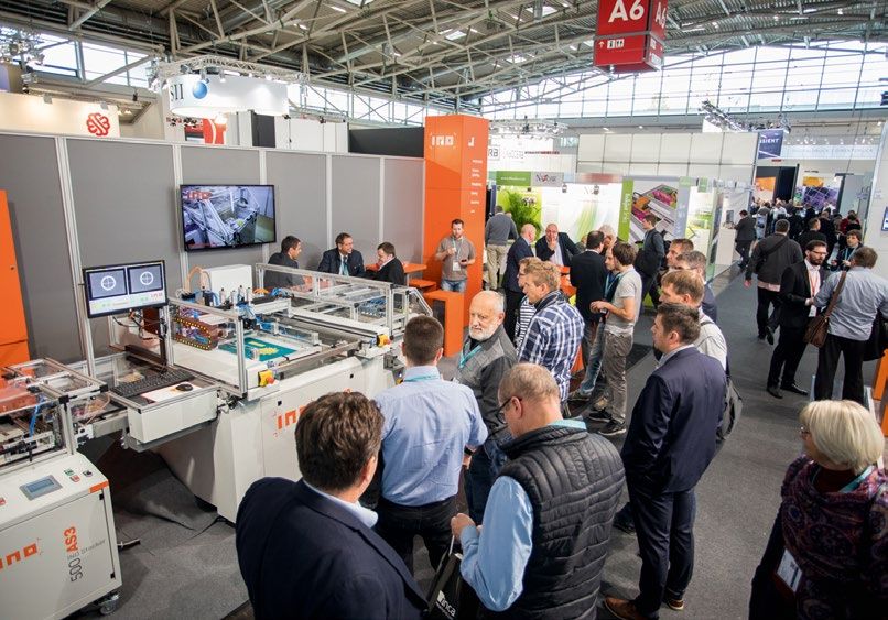
8     GREEN ISSUE

    The greenest energy choice
                                                                                                            renewable energies have to master the tough-
                                                                                                            est and most important battle of the 21st
                                                                                                            century: which is to enable increasing energy
                                                                                                            consumption while generating no further
    Dresden-based Heliatek is convinced that organic                                                        negative impact on global warming. This also
                                                                                                            demands that products are always developed
    photovoltaics (OPV) will play a major role in the                                                       under the condition of minimal environmental
    future of energy                                                                                        impact. Consequently, environmental impacts
                                                                                                            must be quantifiable to set concrete protec-
                                                                                                            tion targets and specific limits to maintain
                                                                                                            the ecological viability of the earth. In par-
                                                                                                            ticular, the environmental profile of energy
                                                                                                            generation should be a part of conscious
                                                                                                            political and consumer-oriented decisions.
                                                                                                            The international standard ISO 14040/44 pro-
                                                                                                            vides a structured, comprehensive method to
                                                                                                            quantify the potential environmental impact
                                                                                                            of material and energy flows throughout the
                                                                                                            product life cycle, the so-called Life Cycle
                                                                                                            Assessment (LCA).

                                                                                                            Life cycle assessment (LCA)
                                                                                                            To evaluate Heliatek's first product, HeliaSol,
                                                                                                            in terms of environmental performance, TÜV
                                                                                                            Rheinland (Germany) undertook a Life Cycle
                                                                                                            Assessment (LCA) study throughout the
                                                                                                            entire life cycle („cradle to grave“) according
                                                                                                            to DIN EN ISO 14040:2009 and DIN EN ISO
                                                                                                            14044:2018. In this study, TÜV Rheinland
                                                                                                            assessed different product layouts with regard
                                                                                                            to their environmental performance: HeliaSol
    Figure 1 – HeliaSol ultra-thin- lightweight, flexible solar film                                        436x2000 (width x length) and HeliaSol
                                                                                                            1270x6000. All environmental impacts were
                                                                                                            evaluated from acquisition of raw materials
        For a sustainable future, the advancing cli-      Climate change – the                              over the production and use up to end-of-
    mate change must be halted. One of the most           global challenge                                  life treatment including all transportation/
    important pillars to achieve the climate pro-                                                           delivery routes. The effect on climate change
    tection goals is the turnaround of the energy         The number of hot days when maximum               is quantified by the impact indicator value of
    sector to low carbon technologies. Heliatek           air temperature exceeds 30°C has increased        CO2 equivalents (CO2e). The CO2 equivalent
    brings an innovative organic solar film solu-         from 3 days (1951) up to 20 days (2018) in        is the result of multiplying the amount of
    tion as a powerful means for the decarbonisa-         Germany [UBA, 2019]. “Warming of the              greenhouse gas (CO2, CH4 and N2O as well as
    tion of the energy sector. Founded in 2006            climate system is unequivocal, and since the      the Kyoto gases NF3, SF6, perfluorocarbons
    by a group of clean-energy enthusiasts from           1950s, many of the observed changes are           (PFCs) and fluorocarbons (HFCs)) by the cor-
    the Technical Universities in Dresden and             unprecedented over decades to millennia.          responding global warming potential (GWP)
    Ulm (Germany), Heliatek now stands on the             The atmosphere and ocean have warmed, the         over a fixed time horizon (see Table 1). The
    threshold of providing the energy market              amounts of snow and ice have diminished,          Kyoto Protocol recommends a time horizon
    with its industrial-grade organic photovoltaic        and sea level has risen” [IPPC, 2014]. Con-       of 100 years. The sum of greenhouse gas
    (OPV) solar film. HeliaSol is an ultra-thin, light-   sequences are increased risks for heat stress,    emissions and removals in a product system,
    weight, flexible all-in-one solution that can         storms and extreme precipitation, flooding,       expressed as CO2 equivalents and based on
    add value to virtually any building surface –         landslides, air pollution, drought, water scar-   LCA is defined as carbon footprint according
    from glass, metal and concrete to polymer             city and storm surges. It is becoming widely      to ISO 14067. Overall, the lower the CO2
    membranes – turning it into clean electricity         recognised in global societies that we have       equivalent value, the lower the potential
    generators, no matter if they are flat, curved        to curb this trend. The exclusive reduction of    impact on global warming and its associated
    or even semi-permanent.                               primary energy demand through decreased           environmental impacts.
                                                          energy consumption is subject to the limits       The carbon footprint results assessed by
                                                          of progressive affluent societies. As a result,   TÜV Rheinland for the use of 1m2 HeliaSol

                                                                                                                   No 28 | September 2019 | OPE journal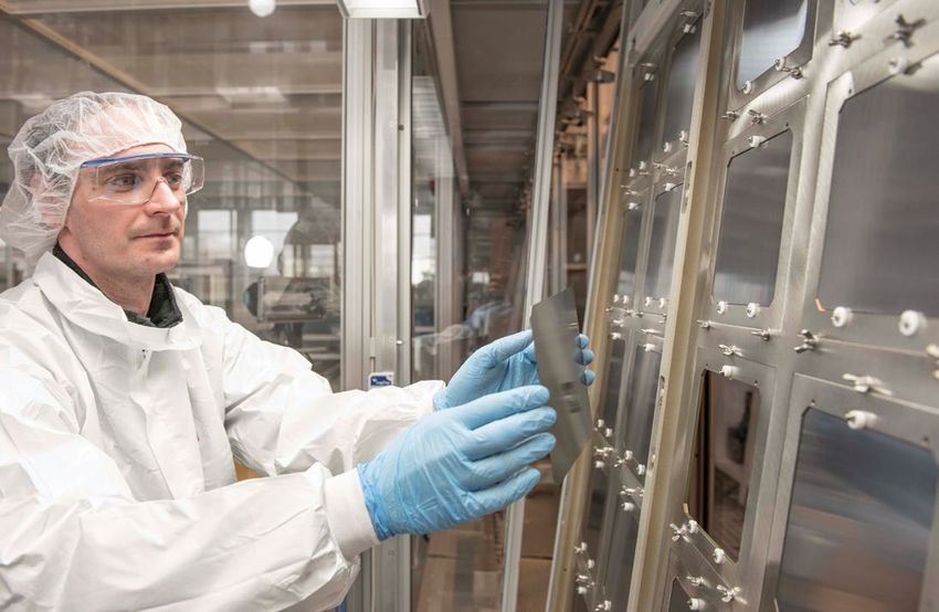
9

                                                                                                       have only a minor impact to the whole life
 Greenhouse gas (GHG)                  Chemical formula                                 GWP100         cycle. The large product HeliaSol 1270x6000
 Carbon dioxide                        CO2                                                         1   has a 9% improved carbon footprint com-
 Methan                                CH4                                                      28     pared to HeliaSol 436x2000 due to a better
 Nitrous oxide                         N2O                                                    265      material efficiency in production. Scenario
                                                                                                       analyses help to identify optimisation poten-
 Nitrogen trifluoride                  NF3                                                 16 100
                                                                                                       tials of specific processes. Due to the high
 Sulphur hexafluoride                  SF6                                                 23 500
                                                                                                       influence of the electricity requirement on the
Table 1 – GWP100 of relevant GHG [IPCC 2013]                                                           CO2 equivalent, the use of green electricity
                                                                                                       for Heliatek production was analysed as a
                                                                                                       scenario in this LCA study. The use of 100%
                                                                                                       green electricity (50% wind and 50% hydro-
                                                                                                       power) would result in a significant reduction
                                                                                                       of up to 25% of the environmental impact of
                                                                                                       climate change.

                                                                                                       Decarbonisation of
                                                                                                       the energy sector
                                                                                                       Decarbonisation is the reduction of green-
                                                                                                       house gas emissions through the transforma-
                                                                                                       tion of the economy, especially the energy
                                                                                                       industry, towards low carbon technologies,
                                                                                                       processes, and products. This is the pathway
                                                                                                       for the internationally agreed target to curb
                                                                                                       global warming to 2°C or less compared to
                                                                                                       pre-industrial levels. Therefore, greenhouse
                                                                                                       gas emissions must be reduced by 40-70%
Figure 2 – TÜV certified carbon footprint results for the use of 1m2 HeliaSol. Calculation based       by 2050 compared to 2010 levels and reach
on 100-year global warming potential (GWP100) values from the IPCC Fifth Assessment Report             close to or below zero by 2100 [IPCC, 2014].
[IPCC, 2013]                                                                                           One of the most important pillars to achieve
                                                                                                       this climate protection goal is decarbonis-
including all upstream and downstream              acquisition. The production process of the          ing energy with low (nearly zero) carbon
processes are presented in Figure 2.               solar film has a share of about 25% with the        technologies.
The highest share of the CO2 equivalent of         main driver electricity for the active layer dep-   The carbon footprint, expressed as CO2
about 50% results from the raw material            osition. Transports (2%) and packaging (5%)         equivalent for the use of 1m2 HeliaSol by

                                                                                                                                                     3A92

                                                                 create
Magazine for Organic & Printed Electronics                         TransFormation                                                   www.conslitter.com
10     GREEN ISSUE

                                                                                                          increase of our solar cell efficiency we will
                                                                                                          bring the carbon footprint of our product
                                                                                                          even further down to become the energy
                                                                                                          source with the lowest carbon footprint in the
                                                                                                          world including hydroelectric, wind and solar
                                                                                                          power. This is a truly green product,” says Jan
                                                                                                          Birnstock, CTO of Heliatek.
                                                                                                          Heliatek is currently building its new produc-
                                                                                                          tion facility for volume production of its unique
                                                                                                          OPV solar films. The production line is planned
                                                                                                          to ramp up in 2020 and will have an annual
                                                                                                          production capacity of up to 1 million m² of
                                                                                                          OPV film at full utilisation.
     Figure 3 – Geographical mapping of the low carbon footprint HeliaSol; aperture efficiency 10%,
     lifetime 20 years, degradation 1% [Conversion using Global Solar Atlas]                              Note: The conversion from kg CO2e/m² to
                                                                                                          g CO2e/kWh was calcutlated by Heliatek.

     TÜV Rheinland offers several advantages. The        the ultra-low CO2e impact of 14.52kg CO2e/
     reference to the module area is not subject         m² enable to payback the greenhouse gas          Written by Susanne Müller,
     to intrinsic dependencies and offers a high         emissions of HeliaSol within a short period of   product development engineer at Heliatek
     degree of robustness in the first step of quan-     2-6 months around the world. This is called
     tification. To relate the carbon footprint to the   carbon payback time (CPT).                       Image sources: Heliatek
     energy generation, the real benefit of a solar
     product, the results have to be converted                                                            Sources:
     into g CO2e/kWh over lifetime. This conver-                                                          IPCC, 2014: Climate Change 2014: Synthesis
     sion allows showing the true environmental              “We are proud to announce                    Report. Contribution of Working Groups I, II
     profile of energy generating technologies. It         the low carbon footprint of our                and III to the Fifth Assessment Report of the
     depends above all on the module efficiency,            Heliatek solutions resulting in               Intergovernmental Panel on Climate Change
     the specific annual yield (kWh/kWp) and                a high CO2e saving potential,                 [Core Writing Team, R.K. Pachauri and L.A.
     the lifetime of a solar module. As a result,            including the disposal at the                Meyer (eds.)]. IPCC, Geneva, Switzerland,
     the carbon footprint varies depending on                                                             151 pp.
                                                             end-of-life of our products.”
     the location of installation. For example, in
     Sweden a solar module can generate about                Guido van Tartwijk, CEO of Heliatek          IPCC, 2013: Climate Change 2013:
     800kWh per kWp-installed capacity per                                                                The Physical Science Basis. Contribution of
     year (specific annual yield), while in Spain a                                                       Working Group I to the Fifth Assessment
     solar module can generate up to 1700kWh                                                              Report of the Intergovernmental Panel on
     per kWp-installed capacity per year. For this                                                        Climate Change [Stocker, T.F.,
     reason, the geographical mapping above (see
                                                         Summary & outlook                                D. Qin, G.-K. Plattner, M. Tignor, S.K. Allen,
     Figure 3) shows the low carbon footprint of         Climate change is happening right now with       J. Boschung, A. Nauels, Y. Xia, V. Bex and
     HeliaSol expressed as CO2 equivalent per kWh        proven negative impact on our environment,       P.M. Midgley (eds.)]. Cambridge University
     across the globe. The map indicates the envi-       economies and societies. The key to slow         Press, Cambridge, United Kingdom and New
     ronmental assessment of one of Heliatek's           down the global warming process is the           York, NY, USA, 1535 pp
     largest pre-commercial products, HeliaSol           significant reduction of greenhouse gases at
     1270x6000 (14.52kg CO2e/m²), including the          all stages of industrial processes. Therefore,   UBA, 2019: Umwelt-Indikatoren; Indikator:
     efficiency ramp until 2021.                         a massive turnaround of energy production        Heiße Tage 2019 [Umweltbundesamt (UBA)
     All in all, this map shows that HeliaSol solar      towards low carbon technologies is essential.    provided by Deutscher Wetterdienst (DWD)]
     films have a carbon footprint ranging from          In order to achieve the climate protection       communication dated 12 June 2019
     3g CO2e/kWh in locations with high solar            targets as soon as possible, the environmental
     irradiation up to 15g CO2e/kWh at some              impacts must be quantified and should be         UBA, 2017: Climate Change 23/2018:
     very few exceptional locations. By displacing       effectively integrated into the competitive      Emissionsbilanz erneuerbarer Energieträger.
     coal and gas-fired power plants from the            process. TÜV Rheinland has certified the         Bestimmung der vermiedenen Emissionen im
     electricity grid [UBA, 2017], each kilowatt-        environmental impact of the pre-commercial       Jahr 2017 [Michael Memmler,
     hour produced by HeliaSol can save 666 up           product HeliaSol to be below 16kg CO2e/m²        Dr. Thomas Lauf and Sven Schneider].
     to 678g CO2e. The higher the CO2e savings           by means of a Life Cycle Assessment. This        Umweltbundesamt, Dessau-Roßlau
     potential, the greater the contribution to the      results in an ultra-low carbon footprint of up
     decarbonisation of the energy sector. Conse-        to 3g CO2e/kWh at many of the high solar
     quently, the high CO2e saving potential and         irradiance locations. “With the continuing

                                                                                                                  No 28 | September 2019 | OPE journal
11
Ultra-short pulse lasers –
improving photovoltaic production
For several laser-based processes in the photovoltaic industry, ultra-short pulse
(e.g., picosecond) lasers can deliver high throughput, improved yields and a superior
final product. These advantages are delivered by a new generation of ultra-short pulse
(USP) lasers that provide a combination of high average power, extremely high
repetition rate and 24/7 reliability
In spite of decades of commercial prod-
uct success and a massive worldwide installed
base, solar energy systems in the form of pho-
tovoltaic panels do not represent a mature
industry – in fact quite the opposite. Multiple
aspects of solar energy continue to evolve,
including semiconductor types and perfor-
mance, module and system architecture, fab-
rication methods, and overall device efficiency.
The motivating factor is economic – the
industry has still not reached the important
tipping point of grid parity, where the true
overall cost of solar generation of electricity
is as low as that of other grid sources based
on hydro, fossil, or nuclear fuels. This requires
multi-pronged approaches – evolution rather
than revolution – that together can lower the
unit cost of solar panels and/or increase their
conversion efficiency
In terms of technology, panels based on
crystalline silicon (c-Si) still represent the
largest market share and generally offer the Figure 1: The fabrication of thin film solar panels involves three separate scribing steps which
highest efficiency. However, thin film PV offers can all be performed by laser
several attractive features that will allow this
technology to compete, namely lower mate-
rial costs and the promise of deployment on panels. Initially silicon was used, but today The main fabrication steps are shown sche-
curved or flexible surfaces. Currently, thin film these devices predominantly utilise cadmium matically in figure 1. The first is deposition of a
devices are produced on a glass substrate, but telluride (CdTe) or copper indium gallium continuous, uniform layer of TCO (transparent
there is a clear road map pointing to flexible selenide (CIGS). However, there are several conductive oxide), with a typical thickness of
substrates and the potential for low-cost roll- critical fabrication steps that are common to a few hundred nanometres, which will form
to-roll production, with some even talking all three types. the front electrodes. A scribe process called
about concepts such as “wrapped buildings.” Each panel starts off as a sheet of glass with a P1 follows, which cuts the entire layer thick-
As a result, many believe that the route to grid typical thickness of 2-3mm that can be more ness. The next step is vapour deposition of
parity will inevitably involve thin film rather than a metre in the longest dimension. This p- and n-type silicon with a total thickness
than c-Si devices. is called a glass substrate, since sunlight will of 2-3µm, again followed by a scribing step
enter through this support glass. A multistep called P2, which cuts through the semicon-
process of vapour deposition and scribing ductor layer. Lastly, a deposition of a thin
Patterning thin films creates low-current active ‘strips,’ typically (sub-micron) metal (Al or Mo) layer forms the
Thin film solar fabrication details vary between only 5-10mm wide, which are electrically rear electrodes. This is then patterned using a
manufacturers, from the choice of semicon- connected in series in order to produce high third scribe process called P3.
ductor material to the size of production power (a few hundred Watts typically).
Magazine for Organic & Printed Electronics12 GREEN ISSUE
The demand for Another issue with nanosecond lasers is that short pulses and high repetition rates enables
precision scribing achieving higher throughput (in order to power scaling without negatively impacting
These scribing steps are particularly demand- lower costs) requires higher laser power. But the HAZ.
ing micromachining applications requiring with nanosecond lasers, increasing the power Lastly, the high peak power of USP pulses
spatial precision and high cut quality. Micro- into the target material is often not feasible means that these lasers can machine thin
cracking, delamination or other peripheral for thin films where the HAZ would become films of even tough materials like carbides and
damage and debris must be avoided as unmanageable. diamond, including materials that are nomi-
these can lead to localised electrical shorts nally transparent at the laser wavelength. And
and reduced device lifetimes. Furthermore, like nanosecond lasers, USP lasers are now
scribe lines should be as narrow as possible USP lasers available at infrared, visible and ultraviolet
to maximise the active area. Again, cost is As a result, the solar industry is increasingly wavelengths, to match different materials
the pre-eminent consideration in fabricating looking to ultra-short pulse (USP) lasers, and focusing requirements; the focus resolu-
thin-film solar panels. Compared to other specifically lasers with pulse durations in tion limit is ultimately determined by a laser’s
mass-produced electronic components such the picosecond range (1ps = 10-12s). There wavelength. Standout examples of today’s
as logic chips and flat panel displays, solar are several advantages to using USP lasers USP lasers include the HyperRapid NX series
cell value per unit area is quite low, making to machine thin films. First, the short pulse of lasers with output powers up to 100 watts.
repair and other rework impractical. The solar duration means that most of the laser pulse These lasers are available as standalone lasers,
industry therefore has a difficult challenge – it energy is ejected with the vaporised material as sub-systems incorporating beam delivery
needs processes that deliver the 24/7 reliability before it has time to spread into the surround- and fast scanning optics and within com-
and high yield of traditional microelectronics, ing substrate. Consequently, under the same pletely integrated tools complete with user
yet it can only sustain one-tenth the cost. conditions, the HAZ is much smaller with a friendly application-specific software, such as
Therefore, speed and throughput are just as USP laser than a nanosecond laser – see the StarCut family from Coherent.
important as precision and edge quality. figure 2. In addition, the pulse energy of
While various manufacturers currently employ USP lasers is orders of magnitude lower than
both mechanical and laser scribing, the tech- with nanosecond lasers. Thus, USP lasers Scribing thin film PVs
nology roadmap points firmly in the direction provide extremely fine depth control which is In terms of material removal, the P1 scribe is
of all-laser scribing. But, what type of laser? important where blind holes or scribes need the least challenging as only a few hundred
to be cut or drilled. The low pulse energy nanometers of TCO are removed, and no
also ensures a much smoother edge quality. other layers are involved. Although quite
Laser scribing Moreover, the ejected particles are smaller demanding on certain laser parameters, it can
Micromachining is best accomplished using and more highly energised, so the amount of be performed using conventional techniques
pulsed lasers where each pulse removes a recast debris is similarly minimised. These are with the near-infrared (1.06µm) output of
small amount of material. Traditionally this important advantages which can be critically a nanosecond laser, such as the Coherent
need has been met by lasers having output important where the economics mean that StarFiber series. But the P2 and P3 scribes
pulses in the nanosecond or tens of nano- post-processing (chemical or physical) should must remove a few microns thickness of
second (1ns = 10-9s) range, and pulse rates be avoided. semiconductor, or the overlaying metal film,
up to 10s or 100s of kHz. These lasers are USP lasers can also deliver high throughput. respectively. The PV industry is now looking
available at infrared, visible and ultraviolet That because while the energy in each at the USP laser for these critical processes.
wavelengths, and today they are widely used individual pulse is very small, USP lasers can The availability of USP lasers at different wave-
in many micromachining applications includ- deliver pulse repetition rates as high as 10s lengths also enables optimisation of a process
ing electronics manufacturing, advanced of MHz. In conjunction with fast scanning called spallation that is an alternative scribing
packaging and display fabrication. However, beam delivery optics, the combination of mechanism for both P2 and P3. Conventional
for very thin layers and films, there can be
limitations to using this type of laser.
With nanosecond pulses, the target material is Figure 2: Laser
heated to vaporisation. But some of the laser micromachining; in
power is conducted into adjacent material drilling, cutting and
texturing applications,
creating a heat affected zone (HAZ). This can
the use of lasers with
take the form of a phase change, microcrack- shorter pulse widths
ing, physical distortion, etc. which can affect avoids some of the
the function of electronic/photonic materials. limitations associated
Moreover, some of the vaporised material with longer pulse
is ejected as particles which remain on the widths, including
thermal effects and
machined surface as recast debris, requiring
recast debris and surface
post-process cleaning. And for thinner films micro-cracking
with a demand for higher spatial resolution, it
is critical to minimise the HAZ.
No 28 | September 2019 | OPE journal13
Figure 3: In spallation, 1) a laser beam passes through transparent layers, 2) it is focused on the interface with a layer that absorbs the laser
wavelength so that rapid heating occurs in a very thin layer, 3) a shock wave expands out, and 4) the target layer is blown off
ablation requires removal of the entire depth of the target layer(s),
which has a somewhat linear dependence on the amount of laser
energy deposited at each location. But a type of laser lift-off called
spallation offers much more efficient removal with less probability of
residual unablated material – see figure 3. These scribes are performed
through the glass and the laser wavelength is chosen to be strongly
absorbed at the junction of the material to be removed. This vaporises
a small amount of material at the film interface, removing the overlay-
ing layers entirely in a micro-explosive effect.
USP processing is proven in c-Si solar
USP laser scribing and cutting has been used successfully in the produc-
tion of c-Si solar cells, for example in creation of openings through
the SiN passivation layer to allow direct electrical connection to the
active semiconductor layer. In some cases, the application needs a
long continuous groove. This can be created by using a beam with a Figure 4: (left) A gaussian profile and overlapping pulses can create a
gaussian profile and then overlapping the pulses – see figure 4 (left). high quality scribe in thin (< 100nm) SiN on silicon.
Tired of wasting silicone?
Fed up with misting?
A breakthrough Solution that eliminates
Misting in Silicone Coating Applications.
Cost savings
Health protection
Increased work safety
Reduced maintenance and cleaning
Elimination of additional exhaust air systems
MISTEX Anti-Misting System for Silicone Coating
Magazine for Organic & Printed Electronics14 GREEN ISSUE
Cutting glass modules
USP lasers are also lowering the cost of
packaging thin film solar modules – namely
cutting the glass modules by a filamentation
process called SmartCleave, which is well
established in other glass cutting applications,
including cutting of strengthened glass. In
simple terms, when a USP laser is correctly
focused into glass, the high peak power
causes an alternating focusing/defocusing
effect which creates a stable filament, leaving
a narrow micro-perforation extending over
several millimeters in depth through the glass.
In order to achieve a continuous cut, these
laser-generated filaments are produced close
to each other by way of a movement of the
work piece with respect to the laser beam.
Filamentation cutting has several advantages
for solar modules. First, it can cut tight curves
and small holes such as the holes needed for
electrical pass-through – see figure 5. Second
Figure 4 (right) Single shot ablation of a 70nm thick SiN layer on silicon using a it creates smooth edges with Ra < 0.5µm, so
HYPER RAPID NX IR laser and a top hat beam optic; each dot is approx. 40 x 40 micrometers very limited polishing, if any, is required. In
and the feedrate is >30m/s addition, it leaves virtually no residual stress
in the edge, unlike conventional glass cutting,
making thin glass products considerably less
vulnerable to breakage during handling,
installation and use. (Glass cracking nearly
always propagates from outer edges due to
residual micro-cracks.)
Summary
The photovoltaic industry is on a relentless
drive to rival the cost of grid power. This drive
relies on continuous efficiency improvements
while simultaneously lowering the manu-
facturing cost. The USP laser, which enables
high throughput, precision processing, is
well-suited to supporting these goals.
Authors: Hatim Haloui and
Joris Van Nunen, Coherent Inc.
joris.vannunen@coherent.com
Figure 5: Picosecond lasers enable the SmartCleave filamentation process that can
cut tight curves in glass, including pass-through holes Image sources: Coherent Inc.
However, some SiN on Si scribing applications no lateral thermal damage to the SiN. In these
must avoid any pulse overlap to completely single pulse applications, the high repetition
prevent any damage to the underlying silicon. rate of the USP laser – up to 5MHz – means
Figure 4 (right) shows an example of this using that the limiting factor is the scan speed.
a beam having a uniform profile shaped using Galvanometer scanners can deliver speeds
a top hat optic. The closely spaced square up to 30m/s, which translates into 1 million
holes in the (15
Shedding light on the sustainable
aspects of printed electronics
In an exclusive interview with OPE journal, Sophie Isabel Verstraelen,
project manager at OE-A, presents the goals and current projects of the
association’s Working Group Sustainability
OPE journal: Ms Verstraelen, can you briefly OPE journal: The environmental factor is
introduce the OE-A Working Group Sustaina- probably not the first thing that comes into
bility to our readers? mind when people talk about organic and
printed electronics. Are we, in fact, a sustai-
Sophie Isabel Verstraelen: As you know, nable industry?
OE-A (Organic and Printed Electronics Asso-
ciation) is the leading international industry S.I. Verstraelen: Determining whether a cer-
association for the emerging technology of tain printed electronics product or technology
flexible, organic and printed electronics. We is sustainable or not is very challenging. This
are representing the entire value chain and depends on many different factors, processes,
provide a unique platform for local and inter- applications, material use, etc. and requires
national cooperation between companies and thorough research. The main impact comes
research institutes. In order to build a stronger from the benefit generated in the application
organic and printed electronics industry, OE-A itself.
covers several important as well as current Here, printed electronics can help creating a
topics and issues. Through a set of working more sustainable world. If you, for example,
groups, we enable and foster collaboration include temperature sensors on food packag-
by all members. One of those working groups ing, you can reduce food waste. By integrat-
deals with sustainability. Sophie Isabel Verstraelen ing organic photovoltaics (OPV) into building
As the organic and printed electronics industry facades you can generate renewable energy.
moves into commercialisation, OE-A believes OLED displays consume way less energy than
that sustainability is an increasingly important traditional ones.
topic. Our Working Group Sustainability aims organic and printed electronics community
to identify and understand the sustainability with information, guidelines and methodolo- OPE journal: OE-A members in your working
benefits of organic and printed electronics gies that will allow members to better under- group came up with a ‘generic printed elec-
technology, emphasising its contribution to a stand the sustainability of their own products tronics device’ containing typical materials
sustainable future in an open dialogue with and processes. that are used in many production processes.
key stakeholders, markets, regulators, and Our comprehension of sustainability is based
wider society. on the principles of safety, economic suc- S.I. Verstraelen: The working group wanted
It is critical that we examine our products cess, fairness, respect & responsibility and to determine the impact of our technologies
and processes to identify how efficiently they includes the dimensions of society, ecology & on the environment. When we contacted var-
are produced, how well we use the materi- economy. We comprehend sustainable action ious recycling companies to ask them whether
als with which they are constructed, and how in terms of the definition of the Brundtland- it would be easy for them to recycle printed
well they use power and other consuma- Report and the definitions of the German “Rat electronics or products including printed elec-
bles when in operation. Finally, when these für Nachhaltige Entwicklung“. tronics, they either were not familiar with the
devices come to the end of their lifetime, we As project manager, I am responsible for this technology or could not tell whether it would
need to identify how they can be recycled or working group. Our core group includes OE-A be relevant for recycling at all. They wanted
dealt with in a responsible, sustainable man- members from both industry and institute: to get more information to be able to bet-
ner. Additionally, the OE-A aims to understand Evonik Creavis – with the Working Group’s ter understand what our products entail and
the key changes in regulations that will affect spokesperson Michael Korell, COPT Center, what our addition to existing waste stream(s)
the industry in the short, medium and long PragmatIC and CPI. But there are more OE-A would be.
term, and how they will harmonise with the members who join our discussions, meetings As printed electronics has a very broad appli-
benefits of organic and printed electron- and projects and provide their input. You can cation range, it is a challenge to just pick one
ics. Moreover, we would like to provide the tell that their interest in this topic is growing! example. That is how we, the OE-A Sustain-
Magazine for Organic & Printed Electronics16 GREEN ISSUE
furthermore be present at K 2019 in Düs-
seldorf (the international industry trade fair
for plastics and rubber) where we will give a
presentation on printed electronics and seek
discussions with various stakeholders explor-
ing and offering alternative solutions.
OPE journal: The Working Group Sustainabi-
lity has also created a Regulatory Framework
in order to raise awareness for international
regulations and standards when it comes to
waste management and material use. Can
you talk about this part of your work?
S.I. Verstraelen: OE-A, together with its
members, has set up a Regulatory Framework
in order to make the printed electronics indus-
try aware of international regulations and
directives as well as standards in the areas of
waste management and material use.
OE-A members need to take into account that
governmental institutions, including e.g. the
European Commission (EC), has put strict(er)
(c) Shutterstock
legislations and requirements in place regard-
ing material use and waste management. The
objectives and targets set in the legislation
have been key drivers to improve waste man-
ability Working Group, came up with the idea then separated and analysed possible critical agement, stimulate innovation in recycling,
to develop (on paper) a ‘generic device’ which materials and created a document with pos- limit the use of landfilling, ban or limit certain
included various printed electronics aspects, sible waste streams for the discussion with the material use and create incentives to change
and which is already – or soon will be – on recycling experts. consumer as well as producer behaviour.
the market. We now have started to have conversations OE-A and its members need to be aware of
Our goal was to develop a quantitative model and meetings with, for example, the plastics these legislations and need to be prepared to
for the impact of printed electronics in waste and paper recycling industry to present and future changes and further restrictions. These
streams resulting from common applications. discuss our findings. We also had a meeting regulations (in particular the ban on certain
We decided upon a ‘generic device’ having with various companies that develop recycling materials) can furthermore put a hold on the
a selection of functional subunits to cover equipment. As a next step we are hoping to further development of certain products and
various options of this technology: A battery- make a recycle trial-run with one of the com- technical applications. This can have a big
powered active sensor label, which periodi- panies to figure out how printed electronics impact on all participants of the process. The
cally measures and stores a temperature, pro- can be recycled and be part of a circular econ- sooner the thin, organic, and large-area elec-
vides NFC communication capability and has omy. Further research remains to be done to tronics (TOLAE) industry is aware of this, the
2 LED indicators, temperature sensor is part of be able to draw concrete conclusions and sooner and easier products and productions
the chip. It contains different components of take the nest steps. It is a complex matter, but processes can be improved and/or adapted.
printed electronics technologies. Such labels we already made quite some progress. In order to inform its members, the OE-A
are already being used in luxury products Working Group Sustainability published the
such as special liquor, but we expect that OPE journal: Sectors such as the packaging OE-A Sustainability Regulatory Framework.
these labels or tags will be soon applied en industry are faced with an enormous backlash Set-up and created by OE-A members, this
masse on, for example, milk packages – this from society due to issues like ocean pollution framework provides the TOLAE industry an
of course increases the use of tags and there- and microplastics in soils and drinking water. overview of the international regulations
fore waste / recycling opportunities. As a next Are members of our industry feeling some of and directives as well as certain standards.
step we identified all the different materials this heat as well? This “living” document (since these regula-
that would be present in this generic device tions and standards are subject to change as
and made rough estimates of their possible S.I. Verstraelen: We are well aware of the they are regularly being reviewed, updated
amounts. All of this we did in small groups current plastics debate. That is also one of or amended, and so is the Regulatory Frame-
of OE-A members and later presented it dur- the reasons we are looking into this topic by, work) serves as an overview and a guidance.
ing various meetings to a broader crowd to for example, talking with the plastic recycling The Regulatory Framework is mapped out
get feedback and input on our findings. We industry and examining regulations. We will along the entire printed electronics life cycle –
No 28 | September 2019 | OPE journal17
from raw materials, equipment and compo-
nents to distribution, user and disposal – to
indicate which regulation or standard might
affect which area. Each indicated regulation
or standard is summarised on a separate
‘one pager’, including a link to more in depth
information.
The overview of the Regulatory Framework is
available to everyone, the complete document
is exclusively available to OE-A members.
OPE journal: What are further fields of
interest for this working group?
S.I. Verstraelen: Besides our participation
at the K tradeshow in Düsseldorf, we are
also collaborating with the VDMA depart-
ment “Plastics & Rubber” and the VDMA
Circular Economy Forum. Moreover, we
support and partner with European Com-
mission programmes and initiatives (e.g.
SmartEES), where sustainability and the
circular economy plays an important role in
technology topics. Finally, we aim at broad-
ening the network with the recycling indus-
try and associations, as well as organising
various meetings on the topic of sustain-
ability, including interactive workshops and
discussions.
Image sources: OE-A
Contact: sophie.verstraelen@oe-a.org
Phone: +49-69 6603 1896
www.oe-a.org A meeting of the OE-A Working Group Sustainability
Visit us
in
Hall 04
Booth
4D45
Erhardt Leimer+
Automation and Vision Systems
ELSCAN – Web monitoring
Proven “dualView“ technology with 2 x 5-megapixel cameras
Intelligent camera (no additional computer)
Image display in Full HD resolution
Remote maintenance access for service
Magazine for Organic & Printed Electronics
Erhardt+Leimer GmbH · Albert-Leimer-Platz 1 · 86391 Stadtbergen · Germany · Phone: +49 (0)821 2435-0 · www.erhardt-leimer.com18 GREEN ISSUE
Oxford PV commercial sized perovskite-on-silicon solar cells
in production, at the company’s pilot line in Germany
The interface between
photovoltaics and printed electronics
Dr Chris Case, chief technology officer at Oxford PV, and Dr Susanne Herritsch,
project manager, VDMA Photovoltaic Equipment, discuss the great opportunity of
perovskite solar cells
The VDMA’s sector association EMINT, Making solar more affordable The importance of efficiency
Electronics, Micro and Nano Technologies, Reliable, affordable and responsibly sourced The cells themselves represent only a small
which was founded in 2014, unites four energy will be a key enabler of smart cities. portion of an entire photovoltaic system,
topics. These four task areas – photovoltaic, As solar and wind become comparable (and which includes the module and balance of
battery production, microtechnologies and cheaper) in price to conventional energy system components (wires, switches, mount-
productronic – are among the most innova- sources, and storage technologies become ing systems, batteries, etc.) Further reductions
tive sub-sectors of mechanical engineering. more cost-effective, renewable energy will in the cost of the cells have a small impact on
These specialist departments work together become an increasingly integral urban inno- the cost of the electricity produced (levellised
with their industrial partners on engineering vation; supporting economic growth, cleaner cost of electricity or LCOE), whereas increas-
solutions for tasks such as autonomous driv- living and mobility, and improved health. ing the efficiency of the cell has a dramatic
ing, renewable energies and electric mobility. The price of solar has dropped by a factor of effect.
The OE-A (Organic and Printed Electronics 200 in the last 40 years, driving its tremendous The solar industry has seen a number of prom-
Association) is also assigned to the VDMA growth. While strong continued growth is ising, high efficiency thin-film photovoltaic
sector association EMINT. forecast, solar accounts for only two percent technologies that strive to take silicon’s place.
As an interface between photovoltaics and of the world’s energy capacity. The challenge Almost all of these have failed commercially,
printed electronics, perovskite solar cells have now is that, while the cost of generating unable to compete with silicon’s relentless
achieved great attention in the last decade. energy with the mainstream photovoltaic reductions in cost. Oxford PV has taken a dif-
With efficiencies, which are already close to solar cell technology – silicon (over 95% of ferent approach. Rather than compete with
those of silicon cells and the advantage, that the market) – continues to reduce slowly, this silicon, its perovskite solar cell technology has
simple production via printing is possible, this is mostly driven by material cost savings, as been designed to enhance the $200 billion
type of solar cell is pioneering. silicon is reaching its practical 25% efficiency silicon solar cell industry.
limit.
No 28 | September 2019 | OPE journalYou can also read