PCI Express 3.0 Compliance Test Seminar and Hands-On Lab - March 8th, 2012 Mike Engbretson, Chief Technology Engineer, GRL Jit Lim, Sr ...
←
→
Page content transcription
If your browser does not render page correctly, please read the page content below
PCI Express 3.0 Compliance Test
Seminar and Hands-On Lab
        March 8th, 2012
        Mike Engbretson, Chief Technology Engineer, GRL
        Jit Lim, Sr. Technologist, Tektronix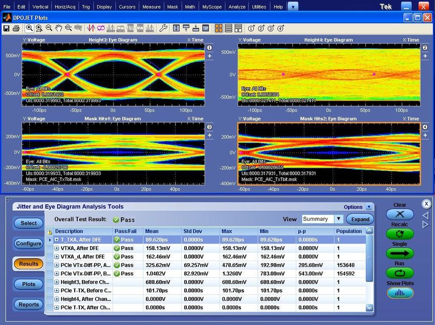
Agenda for the day
9:00am – 10:30am – PCI Express 3.0 CTS Overview and
Introduction to Tektronix Tools
GRL & our involvement in PCI Express (Mike)
Tektronix Tools (Jit)
Lab Overview (Mike)
10:30am – Noon – Lab Session 1
1pm – 2:30pm – Lab Session 2
2:30pm – 4pm – Lab Session 3
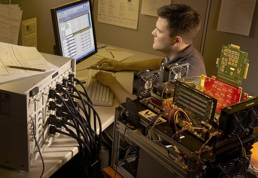
Welcome to GRL, our lab is your lab!
2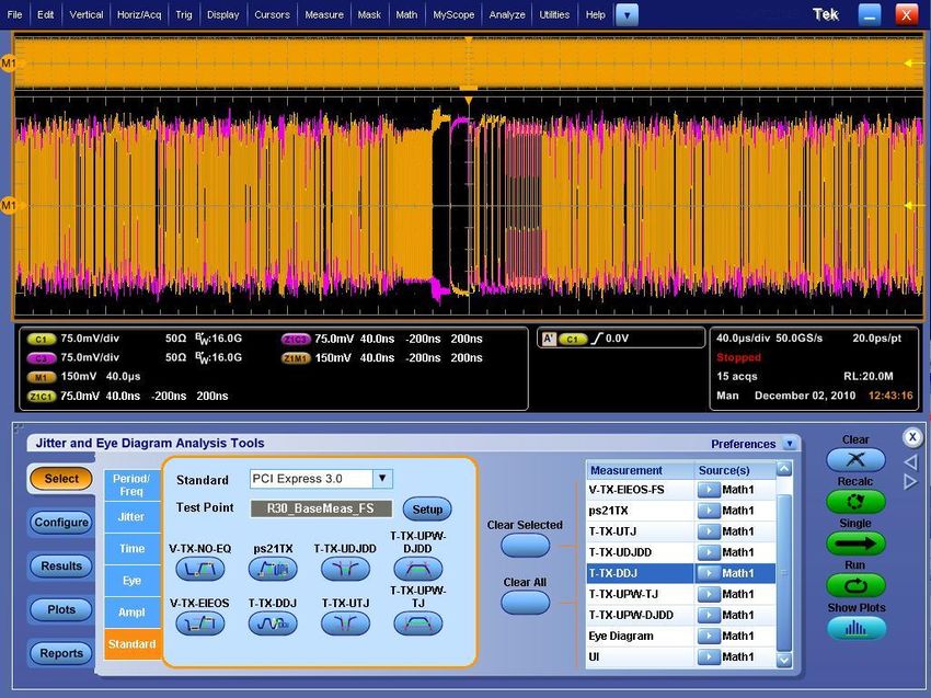
GRL Company Snapshot
Provide test services, reports, & consulting for semiconductor and
electronics hardware companies
Address increasing gap between testing complexity/cost,
customer’s test capabilities, and test equipment solutions
Founded 2009; Headquartered in Santa Clara, CA
Locations in Germany; Hsinchu & Taipei, Taiwan
Focus on high speed connectivity technologies like PCIe, USB,
SATA, SAS, HDMI, DisplayPort, DDR, 10G, MIPI, MHL, Thunderbolt
Services include:
Independent Compliance Testing
-SATA & DisplayPort Official Certification
-Work in process – Thunderbolt, USB3.0, MHL Official Certification
Characterization, Stress Testing & Benchmarking
Signal Integrity Modeling & Testing
Test Methodology Consulting & Training 3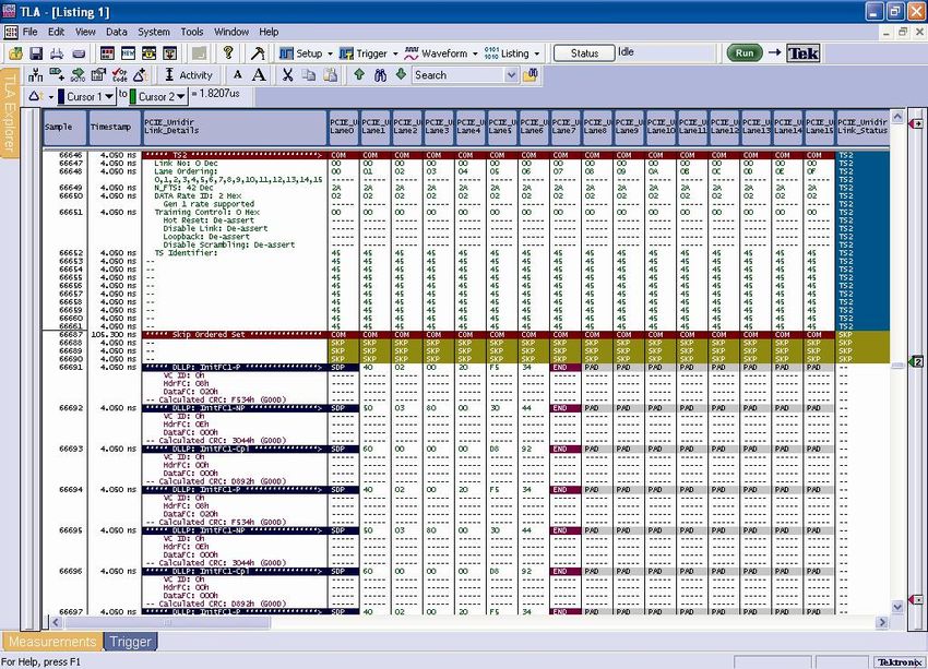
GRLs Involvement in PCI Express
Engineers long standing members of PCI-SIG
Mike Engbretson (Chief Engineer) – 13 years – Tektronix and GRL
Eugene Sushansky (Lab Manager) – 13 years – PLX and GRL
Members of PCI-SIG SEG
Full pre-test capabilities for Gen1/Gen2
Are you ready for the plugfest?
Integrator List Certification happens only at PCI-SIG plugfests
Beyond Compliance
Signal Integrity of PCI-Express Link (Required pre-test for TBT compliance)
Characterization and Stress of PCI Express Silicon Building Blocks
4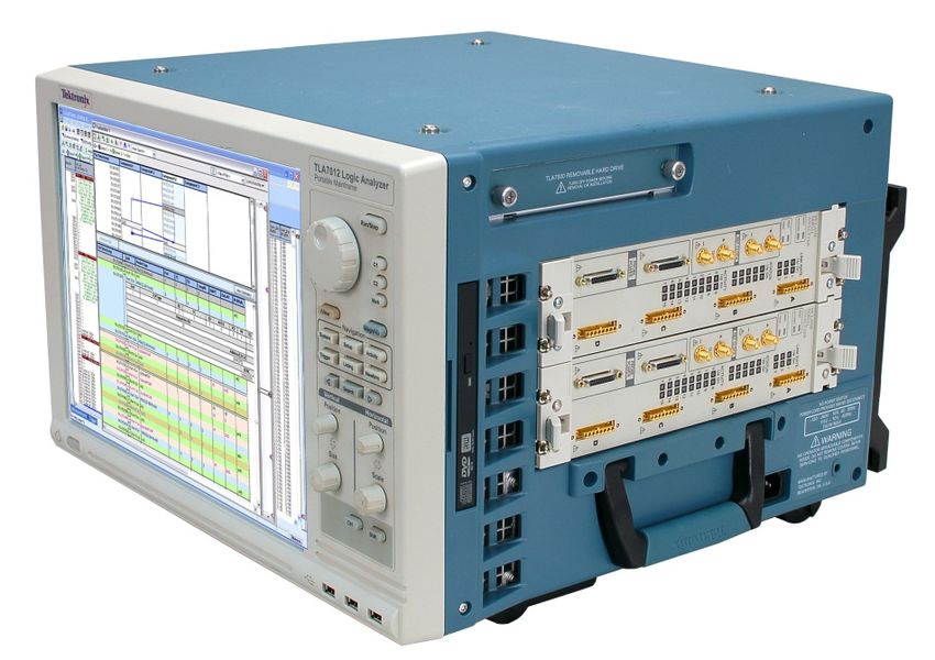
PCI Express PHY CTS
PCI-SIG Has two specifications
Base Specification
CEM Specification
Gen3 CTS 0.7 now in Review by PCI-SIG SEG
PHY CTS is based on the CEM Spec (Systems and Add-In Cards),
testing at the Slot – Compliance Test Point
FYI Period for Gen3 Integrator List Qualification
CTS PHY Tests (0.7)
Transmitter Signal Quality
Receiver Jitter Tolerance
Link Equalization Tests
PLL Bandwidth
Impedance Measurements
5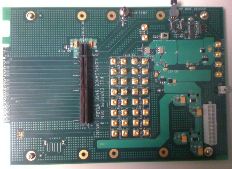
6

Welcome Jit!
PCI Express 3.0 –Physical Layer
Solutions
Estimated Date
  PCI Express 3.0 Technology Timeline                                                                                                                           Released Date

                                    2009                             2010                                        2011                                           2012

                      Q1       Q2      Q3       Q4       Q1       Q2        Q3       Q4          Q1         Q2          Q3          Q4         Q1          Q2       Q3     Q4

                         0.5           0.7                          0.71 0.9         1.0

Base Spec
                               0.5 Release                                            0.7             0.9    1.0
CEM Spec
                                              0.3 Release                                  0.5                                  0.7 0.9                  1.0
Test Spec                                                                                                                                  6 Month
                                                                                                                             FYI Testing   FYI Testing

                                                                                                                                   Deployment Phase
                                                                                     Integration Phase

                                                                                 –     Product Development
                                                                                 –     PCI-SIG Tool Development
                                                            Silicon Phase

                                                            –     CEM Spec Development

       All Information is this presentation is based on 1.0 Base Specification

                     Tektronix Involved in PCIe EWG, CEM, and SEG Working Groups

  8"    4/16/12"
PCI Express 3.0
Trends and Implications         Industry/Technology Trends
                          • 8GB/s using the same board material (FR4)
                            and connectors results in increased channel
                            loss
                          • Probing access at the transmitter pins is
                            typically not available
                          • Receiver equalization can only compensate for
                            channel loss
                          • Receiver Testing is a requirement and is
                            critical to ensure system interoperability
                          • Energy efficiency (Lower mW/Gb/s)

                                             Implications

                          • Link Analysis - de-embedding, embedding, and
                            RX equalization is required post process
                          • Closed data eyes requiring new techniques for
                            transmitter and receiver equalization
                          • Higher data rate signals have less margin –
                            requires de-embedding for base specification
                            measurements
                          • New Jitter Separation Measurements are
                            required
                          • Back channel negotiation to equalize the
                            receiver
                          • Link training and power management continue
                            to be the most difficult logic layer challenges

9"   4/16/12"
10" 4/16/12"
PCIe 3.0 Transmitter Compliance Testing
  •      Compliance testing is based on the
         Compliance Test Specification,
         which is under development
  •      New compliance 128b/130b data
         pattern
  •      Three Tests
             – Electrical: Eye Height and Width
               must pass one pre-set value
             – Preset Test: all Pre-sets are tested
               to be within their limits
             – Transmitter Equalization Test:
               Verify the transmitter will respond
               to equalization change requests
  •      Measurements are taken after the
         Compliance channel and RX
         Equalization using the Compliance
         Base or Load Board
11"   4/16/12"
Transmitter Equalization For Compliance
• Transmitter equalization now requires pre-shoot
in addition to de-emphasis to compensate for
channel loss
• Transmitters must support all defined presets
and a subset for low swing devices
• Presets are toggled on the CLB or CBB the
same way as Gen 2 CLB/CBB
12" 4/16/12"Transmitter Compliance Preset Test
• Validate Vb, De-Emphasis and Preshoot for each Preset are within
spec limits
13" 4/16/12"Add-In Card Compliance Signal Acquisition and Processing
Signal Acquired Embed the Add-In Card Closed Eye due to Apply the Base Open Eye for
from Compliance Compliance Channel the Channel Specification CTLE + Dfe Measurements
Board for Long Channel
System Board Eye Limits 1
Parameter Min Max Units
VTXS 50 1200 mV
VTXS_d 50 1200 mV
TTXS 41.25 ps
Add-In Card Eye Limits 1
Parameter Min Max Units
VTXA 50 1200 mV
VTXA_d 50 1200 mV
TTXA 41.25 ps
1 Measurement Limits Under CEM Review
14" 4/16/12"Serial Data Link Analysis for PCIe Compliance Measurements
• De-embed cables / fixtures
• Embed the effects of the channel
• Equalize the waveform using CTLE,
FFE, and/or Dfe
15" 4/16/12"Embed Compliance Channel
• Verify the channel attenuation
– Based on the PCIe 3.0 Add-In Card Compliance Channel, 10dB attenuation is
expected on high frequency bits (4Ghz for PCIe Gen 3)
16" 4/16/12"Validate Channel Embedding on Scope Waveform
Based on the Insertion Loss Plot, we expect a 10dB loss at the
fundamental frequency of 4Ghz.
– This equates to approx. 68% reduction in the high frequency content of the signal (lin = 10^(db/20), so
10^(-10/20) = .316)
This can be easily verified on the scope waveform by doing a quick
check using cursor measurementsValidate Channel on Scope Waveform Next measure the vertical amplitude after the channel (approx. 140mV) SDLA has automatically applied the channel filter to Math 4
Receiver Equalization

  •      PCIe reference equalizer is CTLE and 1 Tap DFE
           –     CTLE – one Zero and Two Poles
           –     DFE – 1 Tap (-30/30mV tap value)
  •      Equalizer is optimized on the CTLE + DFE tap value that results in the best
         eye area
           –     7dB Adc settings are shown in the example below

19"   4/16/12"
Automated Receiver Optimization
• Manually optimizing over 7 CTLE settings is time consuming
• Optimization is automated with SDLA
• Optimization is done on a short record across all settings, the setting
with the best eye opening is then computed and measurements can
be taken
20" 4/16/12"Verifying Effects of RX Equalizer
• Low frequency bits are attenuated based on the optimal CTLE setting
• Example below shows plot of -8dB Adc
– Low frequency bits should be attenuated by ~60%
• DFE will result in an increase of eye opening based on the tap value
setting
21" 4/16/12"Validate Equalizer: Analyze Raw Waveform On the scope, use cursors to measure the low frequency content of the signal on the acquired waveform (Math 1) In this example the low frequency content of the waveform is approx. 615mV
Validate Equalizer: Analyze Waveform After CTLE Based on the CTLE that was applied, we expect a 60% attenuation in the low frequency content after the CTLE This can quickly be verified, note the low frequency amplitude is approx. 240mV
Validate Equalizer: Analyze DFE
The DFE will open the eye by twice the tap value
PCIe uses a 1 tap DFE, meaning that the previous bit will determine
if change of the current bit.
The table below outlines the change based on the 20mV Tap
Previous Bit Current Bit Change
0 1 20mV
1 0 -20mV
0 0 No Change
1 1 No ChangeValidate Equalizer: Analyze DFE DFE will open the eye by approx 2 times the tap value High frequency signal before DFE is 126mV and after 166mV, which is 2 times the tap value of 20mV
CEM Measurements with Optimized RX Settings
•     CEM measurements can by quickly done with pre-defined setup files in
      DPOJET
•     Simultaneous assessment of the signal at each point during the post
      processing stage

26"   4/16/12"
Testing Beyond Compliance
• What happens if a measurement fails SigTest?
• Could it be the channel?
– Measurements can be taken before the channel
to evaluate results
– Different channel models can be created using
Serial Data and Link Analysis
• How does the optimized RX setting compare to
other settings?
– Easily compare the results of multiple
Equalization settings
• Does deeper analysis of the waveform need to
be done?
– PCIe specific measurements can be taken in
Tektronix’ measurement system DPOJET
– Determine if data dependent, uncorrelated or
pulse width jitter is in spec
– Measurements filters and settings can be
adjusted to get to root cause, but remember you
must pass SigTest to be certified for compliance
• Is the TX compliant?
– NEW PCIe 3.0 base spec measurements are
available to verify TX compliance
27" 4/16/12"Base Specification Transmitter Measurements
• Base Specification Measurements are defined at the pins of the transmitter
• Signal access at the pins is often not assessable
• De-embedding is required to see what the signal look liked at the pins of the
TX, without the added effects of the channel
• Sparameters are acquired on the replica channel
Signal at TX Pins Measured Signal Apply Sparameters Signal with Channel
at TP1 Effects Removed
28" 4/16/12"De-embedding Considerations 5 GHz 10 GHz
• De-embedding amplifies high frequency
noise, thus requiring a bandwidth filter
– This also impacts the required bandwidth for a
RT Scope
– Bandwidth is dependent on board material
• Successful de-embedding starts with good
quality board design and S-Parameter data
– Matched impedance, low loss structures
– No gain, significant resonances, or large dips
• Quality of de-embedding
5GHz Filter 10GHz Filter -> Noise amplification
– Eye height and jitter
– Signal to
Noise Ratio
29" 4/16/12"Verification of De-embedding Results
• Best to have original signal at the TX pins
• Embed the sparameter representing the test fixture
• De-embed the sparameter representing the test fixture
• Compare the waveform as acquired from the DUT directly with the fixture
embedded in the original waveform
– Captured Waveform (White), Channel Embedded in Direct Waveform (Yellow)
30" 4/16/12"De-Embedding Results
• Good correlation is shown below- verify rise time, pre-shoot/under-shoot,
ripples
• Signal at TX pins – white
• Signal at TP1 – blue
• Signal after de-embedding from TP1 – Red
31" 4/16/12"Further Analysis on Gen 3 Measurements • Acquired Signal (Left) • De-embedded Signal (Center) • Signal at TX Pins (Right) • All Gen 3 Base Spec Measurements done on de-embedded waveform 32" 4/16/12"
NEW PCI Express Base Specification Measurements

  •      Voltage
  •      Package Loss
  •      Transmitter Equalization
  •      Jitter

33"   4/16/12"
Transmitter Equalization Measurements
VTX-BOOST-FS / VTX-BOOST-RS
•     What’s new for Gen 3.0
        –        De-Emphasis (Va) and pre-shoot (Vc)
        –        Transmitters must support 11TX equalization pre-sets
•     The high frequency nature of 8.0 GT/s signaling
      makes measurement of single UI pulse heights
      impractical due to attenuation by the package and
      breakout channel
        –        Amplitude measurements are taken on low frequency
                 waveforms (64 ones/ 64 zeros in the compliance
                 pattern) using last few UI of each half period
        –        Va and Vc values are obtained by setting the DUT to
                 a different preset value where the desired Va or Vc
                 voltage occurs during the Vb interval.

34"   4/16/12"
Transmitter Voltage Measurements
VTX-EIEOS-FS / VTX-EIEOS-RS
• Launch Voltage of Electrical Idle Exit
Ordered Set
• Required to ensure that the RX can
properly detect an exit from electrical idle
• Taken on a pattern of eight ones
followed by eight zeros repeated 128
times included in the compliance pattern
– Taken on the middle five UI to reduce
attenuation effects of the channel
• VTX-EIEOS-FS - Full Swing Signaling
– Measured by Preset 10
• VTX-EIEOS-RS – Reduced Swing
Signaling
– Measured by Preset 1
35" 4/16/12"Package Loss Measurements
PS21
• Can be taken at TP1 while capturing silicon package loss and drive
characteristics, but due to the high frequency content of the 1010 pattern
the measurement must be de-embedded back to the TX pins
• Measured by comparing 64 zeros and 64 ones PP voltage against a 1010
pattern
• Measured with de-emphasis and pre-shoot set to 0 at the end of each
interval to minimize ISI and low frequency effects
36" 4/16/12"Transmitter Jitter Measurements
• Necessary to take transmitter jitter measurements with all lanes operating in
order to capture crosstalk effects
• Measurements are taken at TP1 and de-embedded back to the pins of the TX
• Necessary to separate uncorrelated and data dependent jitter in order to
ensure that jitter that can be recovered is not budgeted as uncorrelated jitter
Jitter measurements Data Dependent Jitter Uncorrelated Jitter
Cause Due to package loss and Uncorrelated - PLL jitter,
reflections (dynamics in the crosstalk, noise conversion
channel, ISI) (amplitude to phase)
How to compensate Can be reduced by Difficult to remove (better
equalization components, layout)
37" 4/16/12"Transmitter Jitter Measurements: Data Dependent Jitter
TTX-DDJ
DDJ Measurement Process
• Measurement taken on multiple repeats of the compliance pattern using a 1st
order CDR function representing a high pass filter
• A PDF is created for each edge crossing of the compliance pattern
• DDJ is calculated as the difference of the mean of each PDF and the recovered
clock edge
• Measurement is defined as the absolute value of DDJ(max) – DDJ(min)
38" 4/16/12"Uncorrelated Jitter Example
TTX-UTJ / TTX-UDJDD
• DDJ is removed from the PDF of
each edge
• Data is converted to Q-Scale
• Uncorrelated Deterministic Jitter
Dual Dirac (UDJDD)
– Accounts for Periodic Jitter and
Crosstalk Convert the PDF to Q-
Scale
• Random Jitter is implied by
subtracting UDJDD from UTJ
39" 4/16/12"Uncorrelated Total and Deterministic PWJ
TTX-UPW-TJ / TTX-UPW-DJDD
• Pulse Width Jitter
– Addresses lone bits that are attenuated
the most in lossy channel and could
likely cause bit errors
• DDJ is removed to accurately quantify
PWJ
• Calculate edge-to-edge jitter
• Construct Q-scale PDF curve and
Extrapolate to BER = 10-12 (Q= 7.03) to
determine Uncorrelated Pulse Width
Jitter (containing F/2 or Odd/Even Jitter)
and Deterministic Pulse Width Jitter
• Final measurements are calculated by
looking at the left hand side of the PDF
curve
40" 4/16/12"Tektronix Solutions for PCI Express 3.0 Measurements
• Visibility
– Tektronix is the only scope vendor that provides visibility of the link at multiple
test points.
– Unlike other solutions Tektronix provides a complete set of Base Specification
measurements with associated plots for characterization, debug, and analysis
– Complete insight into all possible equalization settings for comparison and debug
• Flexibility
– Customers can quickly verify their measurements with different configuration
settings, unlike other solutions
– Other solutions are targeted at compliance, however, with DPOJET customers
can quickly debug root cause of problems in a standard specific environment
• Compliant
– Equalization follows the requirements in the specification, unlike other vendors
who have a single methodology for applying a DFE
41" 4/16/12"Tektronix BSA85C Bit Error Rate Tester 42" 4/16/12"
Agenda 1.Introduc+on 2. Stressed Eye 3. Beyond Compliance 4. Receiver Test Demonstra+on PCI Express is a trademark of PCI-‐Sig, www.pcisig.com USB is a trademark of USB-‐IF, www.usb.org 43
Introduction
• Latest
Genera+on
Add-‐In
Card
Computer
Standards
have
some
common
trends.
• We’ll
use
PCI
Express
Gen
3
as
our
main
End
Point
example
• Similar
themes
are
PCI
Express
emerging
in
other
new
Gen
3
Link
standards
such
as
IEEE
100GbE
etc.
Host
or
Root
Complex
Motherboard
44Introduction - Basics At
the
simplest
level,
receiver
tes+ng
is
composed
of:
1. Send
impaired
signal
to
the
receiver
under
test
2. The
receiver
decides
whether
the
incoming
bits
are
a
one
or
a
zero
3. The
chip
loops
back
the
bit
• PaNern
Generator
stream
to
the
transmiNer
• Stress
4. The
transmiCer
sends
out
exactly
the
bits
it
received
• Error
Counter
5. An
error
counter
compares
the
bits
to
the
expected
signal
and
looks
for
mistakes
(errors)
45PCI Express 3.0 Equipment Setup
Product: Silicon, Host, and AIC solutions from the BERTScope portfolio
Industry Knowledge: Participation in standards meetings
Technical Expertise: Plugfest, Intel testing events
Host Testing Add-in Card Testing
46Agenda
1. Introduc+on
2.Stressed
Eye
• Changing
Test
Signal
Recipes
• Channel
Considera+ons
3. Beyond
Compliance
• Calibra+on
Challenges
47Receiver Testing (a.k.a “Jitter Tolerance”)
Review
Test
receiver
for
error
free
operaFon
(0
BER)
while
stressed
with
input
jiCer/impairments.
Calibrated
jiCer/stress
is
added
to
PaNern
Generator
(PG),
output
is
increased
un+l
receiver
experiences
bit
errors,
or
test
limit
is
reached.
Test
oVen
repeated
at
another
jiNer
frequency,
results
are
ploNed.
PaCern
Stress
Generator
Impairments
PaNern
High
Speed
Amplifiers
etc.
48Receiver Testing (a.k.a “Jitter Tolerance”)
Review
Test
receiver
for
error
free
opera+on
(0
BER)
while
stressed
with
input
jiNer/impairments.
Calibrated
jiNer/stress
is
added
to
PaNern
Generator
(PG),
output
is
increased
un+l
receiver
experiences
bit
errors,
or
test
limit
is
reached.
Test
oVen
repeated
at
another
jiNer
frequency,
results
are
ploNed.
PaCern
Stress
• Stress
recipe
varies
by
Generator
Impairments
standard.
In
theory
it
emulates
the
system
impairments
for
the
expected
use.
PaNern
High
Speed
• Higher
data
rates
mean
closed
Amplifiers
eyes
and
crosstalk
are
bigger
etc.
issues.
49PCIe Gen 3 Stress Recipe PCIe
3
- Overview USB
3
PCI
Express
Gen
3
uses
a
long
circuit
board
channel
that
closes
the
eye,
and
two
forms
of
ver+cal
Tx
Eq
eye
closure
(‘Interference’).
8G
PRBS
Cal.
Replica
Test
Combiner
Gen
Channel
Channel
Equipment
Post-‐
RJ
SJ
processing
Source
Source
Diff
CM
Interference
Interference
Eye
Height
Adjust
(Taken
from
PCI
Express
Base
Spec,
Figure
4-‐71)
50PCIe Gen 3 Stress Recipe PCIe
3
- Channel USB
3
• Depending
upon
Host
or
Add-‐in
Card,
different
test
fixtures/
Tx
Ea
combina+ons
q
re
used.
• ISI
is
large
8G
enough
PRBS
to
mean
the
Cal.
Replica
Test
Eye
is
closed
Combiner
at
the
receiver.
Gen
Channel
Channel
Equipment
Post-‐
RJ
SJ
processing
Source
Source
Diff
CM
Interference
Interference
EH
Adjust
51PCIe Gen 3 Stress Recipe PCIe
3
- Calibration USB
3
Long
waveform
capture
by
Real
Time
Scope
Tx
Eq
8G
PRBS
Cal.
Replica
Test
Combiner
Gen
Channel
Channel
Equipment
Post-‐
Post-‐processing
RJ
by
SJ
soMware.
processing
Several
complex
Source
e lements
are
accommodated
in
Source
soVware
including
the
IC
package
and
elements
Diff
CM
within
the
IC
including
the
equalizer.
Interference
Interference
EH
Adjust
This
is
s6ll
in
flux
–
Correla+on
work
ongoing
between
simula+on
and
direct
measurement
and
analysis
techniques.
Being
refined
at
Plugfests
52PCIe Gen 3: Example Gen
3
CBB
Riser
PCIe
3
Add-In Card Stress Calibration USB
3
Gen
2
CLB
SI
Combiner
Rx
Lane
0
+
+
In
Out
-‐
-‐
Gen
3
CBB
(Main)
Tx
Lane
0
To
RT
Scope
for
calibraBon
Last
Cal.
details
being
refined.
This
setup
being
successfully
used
at
Plugfests
53Base Spec calibration recommendation
SigTest or DPOJET
– PCI-SIG group methodology
– Repeatable
– Easy to understand
– Used for Tx testing
54 Tektronix Confidential BERTScope Products OverviewPCIe
3
Loopback – PCIe 3 USB
3
• PCIe
3
loopback
is
more
complicated.
1. Speed
negoFaFon
–
na+vely
2.5GT/s,
“Brute
Force”
needs
to
nego+ate
up
to
8GT/s
paAgenda 1. Introduc+on 2. Stressed Eye 3.Beyond Compliance When a Device Fails… What Next? 56
Beyond Compliance
BERTScope = Debug/Characterization
1.
Click
a
control
3.
Changes
buCon
in
the
UI
2.
Adjust
happen
instantly
Easy
adjust
with
turn
of
the
knob
You
may
need
to
try
lots
of
different
signal
condiFons
May
want
to
monitor
BER
while
changing
stress
condiFons
on
the
fly
57Beyond Compliance
The BERTScope Analysis Tools
Besides
being
a
BERT,
the
BERTScope’s
“Scope”
funcFonality
brings
benefits
that
complement
those
of
the
Tektronix
scopes
Analysis
tools
are
full
featured
and
easy
to
use
Frees
up
the
scope
for
other
tasks
Eye
diagram
for
quick
diagnosis
of
synchroniza+on
and
BER
failure
issues
Debug
challenging
signal
integrity
problems
Error
LocaFon
Analysis
PaCern
Capture
JiCer
Map
BER
Contour
58Summary High
Speed
Receiver
Test
Solu+ons
from
Tektronix:
Higher
speeds
on
cheap
channel
BERTScope
Family
materials
causing
closed
eyes
from
ISI
and
crosstalk
Increased
use
of
equalizaFon
forcing
changes
in
tes+ng:
speed,
equaliza+on
nego+a+on
&
Tx
control
Test
signal
is
changing:
VerFcal
eye
closure
Closed
eye
CalibraFon
is
evolving
ANaining
Loopback
is
oVen
problemaFc.
Returned
signal
is
oVen
also
a
closed
eye,
meaning
eye
needs
opening
before
error
coun+ng
59One Tool to Span from Protocol to Physical Tektronix TLA7SA00 Series
Logic Protocol Analyzer for PCI Express
TLA7SA00 Series supporting PCIe Gen 1 through Gen 3, Protocol through Physical layer
Information Density for Rapid Analysis
– Transaction Window with BEV Flow control
– Summary Profile Window
– Lane-by-Lane decode with Listing Window
Shortened Time to Confidence
– Front panel status LEDs
– Auto Configure capability
Powerful Triggering and Filtering
– Trigger on Events from Physical to Protocol
– Real-time Filtering
Recognized Probing Leadership
– Probe anywhere on the bus using OpenEYE
technology
– Flexible probing solutions including legacy
probe support
– ScopePHY provides PHY layer access to
oscilloscope through LPA probes
– Link Tracking including superior ASPM
support with FastSYNC
Multi Bus visibility for system level debug
– Support multiple PCIe links used in switch or
bridge applications
– Cross Bus correlation/triggering
– DDR, QPI, DMI, PCIe & others
Accelerated Time to Actionable Information
–Information Density Transaction stitching shows packets participating in transaction – or
incomplete transactions as errors – mouse over shows time –
arrowheads/squares filled or not based upon completion
Transaction Window
BEV
Toolbar (Bird’s Eye
(Search, View) New
filter, display visualization
management unique to LPA
)
View finder region
Status bar &
access to
“Summary
Statistics Panel for
Profile
Flow Control
Window”
including Roll
Over report of
Credits consumed
Each row of
the Packet
View pane
represents a Transient Event
single packetInformation Density
Summary Profile Window
1 or more
Links
“At a glance” review of
Summary Sparkline's (divides
statistics acquisition memory into 100
slices or centiles) provides
key information such as
Trace health and behavior of bus
elements
view
Each
protocol
element
represented
with its
statistics
Visually see training occur by
1st
recognizing patterns.
occurrence
hyperlink
63Information Density
Listing / Waveform windows
Lane by Lane
Decode
Packet
Decode
Ability to
view only
Packer
headers Time
Correlated
Analog Data
from Scope
using power
of iView
Waveform
symbolic
decode
(lane
alignment
disabled for
accurate time
correlation)Shortened Time to Confidence
TLA7SA00 Setup Window Most recent
Calibration
Statistics and
access to
calibration
summary
Real-time Link
Automatically
Speed and
track / Manually
Status
setup, Link
Information
Speed, Link
width, polarity etc.
Configuration
screen reflects
front-panel
LED lane
status
Module “wires” itself
automatically based on
observing signals yet
allows user to adjust
wiring
Easy Access to
Triggering,
Filtering and
Additional HW
settingsCalibration
Single click calibration,
– System will perform calibration,
unattended for as long as
necessary
System recognizes when
configuration has changed
– Informs user of need to calibrate
– Permits calibration on selected
lanes only
Permits variable BER target
– If target can’t be met, calibrates to
best BER resultPowerful Triggering and Real-Time Filtering
Packet level triggering
– 8 states
– 8 packet recognizers
– 4 symbol sequence recognizers
– 4 counter/timers
– 4 event flags
Pre-defined trigger templates
(trigger on any field within
packet)
Real-time filtering of selected
packet types
Store only data of Interest
Efficient usage of memoryProbing Leadership
OpenEYE and FastSYNC
Unequalized Rx signal @ 8 GT/s Equalized Rx signal @ 8 GT/s
24” channel w/ 2 connectors 24” channel w/ 2 connectors
Tektronix probes utilizes OpenEYE Technology that incorporates automatic
tuning equalization circuitry to recover PCIe Gen3 signal
– Mitigates the wide spectrum of losses encountered by probing at different points on
the channel
– Automatically adapts to being attached at any location on the channel
Tektronix FastSYNC utilizes proprietary technology to ensure our
1 2
reschronization time to beProbes Tektronix Probing Solutions for PCI Express Slot Interposer Midbus Probe Solder-Down Probe Available in x16, x8, x4, x1 link Available in x8 or x4 link widths (2 High-performance solder-down widths for x16) probing of one PCIe3 differential pair Appropriate Lane Converters are Rugged probe head with contacts Compatible with P7500 Series included with each Interposer for contained in retention module TriMode probing leadsets that can probing smaller link widths thus be shared with an Oscilloscope increasing the value of the interposer Bracket for SUT end point card Midbus probes also available for provides mechanical stabilization legacy x8 and x4 PCIe2 midbus and reliable connection footprint 6’ probe cable, Ships in antistatic, foam-lined, plastic case 69
ScopePHY™
Quickly Scope PCI Express PHY Layer
TLA7012 2x TLA7SA16
2-module x8 PCIe3
logic Modules
analyzer
mainframe Quickly connect any of the probe
connector outputs to an oscilloscope
– Midbus, slot interposer or solder-down
DPO/DSA Enables you to answer:
72004B
4-channel 1. Is the probe functioning properly and
20 GHz faithfully delivering my PCIe 3.0 signals to
oscilloscope the module?
with
DPOJET 2. Does my PCIe 3.0 signal meet probe input
loaded with requirements?
P67SAxxx 3. Is my probe connected properly to SUT?
S-parameter
file to
de-embed
Tek-supplied S-parameters of probe
the probe +module configure a Tektronix
oscilloscope’s DSP filters to show the
PCIe3 data eye @ the probe tip
P67UHDSMA
2-lane probe leadset (8 low-
loss coax, each with 50 ohm TCA-SMA TekConnect Adapters shown
terminator connected to 1-lane (2 differential inputs)
out of the 2-lanes per P67SAxxx probe
connector. Unconnected lanes have 50ohm
terminators connected at end of coax.Multi-bus Visibility with Single GUI & Mainframe
TLA Expansion with TekLink
TLA7012 2-module mainframe TLA7016 6-module mainframe
Shown with 2 TLA7SA16 modules Shown with 2 TLA7SA16 modules for x16 PCIe3 link & 2
for x16 PCIe3 link TLA7BB4 modules for 2 channels DDR3-1600
Portable mainframe with integrated Benchtop mainframe with GbE controller
15” display and PC controller
Connects to PC via GbE for running TLA
Connects to PC via GbE for running Application Software
TLA Application Software
Up to 8 frames interconnected via TekLink
2 frames connected directly
via TekLink cable
3-8 frames require TL708EX
8-port TekLink hub
TL708EX
8-port TekLink hubResources
New!
USB3
55W-‐2
6804-‐0
Extensive
applica+on
PCIe3
-‐2 7105-‐0
informa+on
at:
55W
www.tek.com
PCI
Express
:
PCI-‐Sig,
www.pcisig.com
USB:
USB-‐IF,
www.usb.org
72Important Resources
• Complete Solutions Available on www.tek.com
– Solutions available today for PCIe 1.0, 2.0, 3.0
Transmitter, Receiver, PLL Loop bandwidth and
Protocol Testing
• Support & Resource Links
– Recommended Equipment Configurations
www.tek.com/serial_data
– Access to new PCE3 Software Downloads & Free Trial
www.tek.com/software (search for PCE3)
– PCI Express Base Specification (members only)
http://www.pcisig.com/specifications/pciexpress/
73"
73
" 4/16/12"75 Lab1:System Transmitter Lab
System Setup
Equipment List
System DUT
Power Supply
with power on ‘McGyver tools’
System Fan to keep system cool
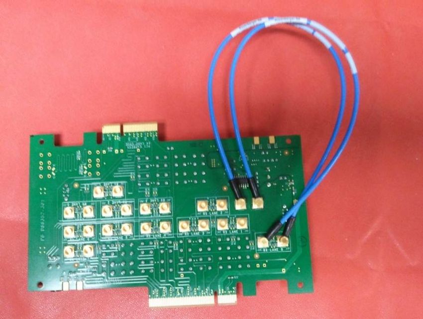
PCI Express 3.0 Load CLB3
2 ea. SMP Cable pairs
1 ea. pair of SMP patch Cables
76CLB3 Load Board Configuration
X16 Connector
Interface
Lane0 Differential
Data Acquisition
Ch1-Ch2
Data Pattern Toggle
X1/X16 RefClk Switch
Differential Clock
Acquisition
Ch3-Ch4
Toggling Features
RefClk Source Toggle
Patch Cables
77X16 Compliance Test Flow Capture 14 Waveforms on Lane0 Tests to Run 1. 2.5GT/s - Captured at 2Meg RL 1. Lane0 - Run Preset level 2. 5GT/s – Captured at 10Meg RL verification on Waveforms 3. 5GT/s – Captured at 10Meg RL 4-13 using SigTest 4. 8GT/s Preset0 – Captured at 10Meg 5. 8GT/s Preset1 – Captured at 10Meg 2. Lane0 - Run Eye Diagram 6. 8GT/s Preset2 – Captured at 10Meg Signal Quality on 7. 8GT/s Preset3 – Captured at 10Meg Waveforms 1-4, 7, 8. 8. 8GT/s Preset4 – Captured at 10Meg 9. 8GT/s Preset5 – Captured at 10Meg Must pass 1-3 and one 10. 8GT/s Preset6 – Captured at 10Meg 8GT/s Preset 11. 8GT/s Preset7 – Captured at 10Meg 12. 8GT/s Preset8 – Captured at 10Meg 3. Repeat Step 2 on 5ea. 13. 8GT/s Preset9 – Captured at 10Meg Populated CLB3 Lanes 14. Confirm DUT Returns to 2.5GT/s
Scope Setup
1. Choose Horizontal > Setup Menu

2. Select Constant Sample Rate

3. Increase Scale to 4.0us (2.0M Record Length), menu:

4. Select Horizontal Zoom

5. Select Setup

6. Adjust Horizontal Zoom Factor to 5000

7. Close Zoom1 Setup Menu, result of display should be:

                                                          79
Acquiring Data 1. Slide RefClk toggle switch such that RefClk is not being displayed on the scope. 2. Push the data pattern toggle button Once such that the pattern changes to 5GT/s. 3. Return switch to position that displays both Data and RefClk at 5GT/s. 4. Press Single on the Scope front panel to capture the waveforms. 80
Processing Data with SigTest
1. Run SigTest 3.1.69 from the
Scope’s Desktop
2. To test 2.5GT/s signal Browse to
the Data signal you captured
using Differential as the Data
Type
Note for 2.5GT/s, only Data
waveform is tested.
3. Press Load and Verify Data File.
4. Select pcie_cem_sys_1_1 as
Technology.
5. Select TX_SYS_CON as
Template File
6. Press Test
81Testing Presets with SigTest
1. Test only needs to be run on Lane0 for
Compliance.
2. Run SigTest 3.1.69 from the Scope’s
Desktop
3. Select the Preset test button
4. Browse and load the Preset4 (P4)
waveform as indicated by the Testing
table
5. Press Test
6. Highlight the field for the next waveform
to be loaded.
7. Repeat steps 4 and 5 for waveforms P1-
P10 in the order indicated
8. Review results once complete
82Lab2: PCI Express 3.0 System Receiver Test Lab Mike Engbretson, Chief Technology Engineer, GRL
SystemCard Test Setup
Equipment List
1 ea. DUT
1 ea. PCI Express 3.0 Load Board (CLB3)
1 ea. PCI Express 3.0 Repeater
3.3 Power Supply
1 ea. SI Combiner
1 ea. ATX Power Supply
2 ea. set of matched SMP Cables
4 ea. sets of matched pair SMA Cables
1 ea. SMA 12” SMA Cables
1 ea. 72” BERTScope cable
1 ea. Clock Multiplier
84BERTScope Setup
3. Select the Generator View
(View Generator)
4. Click on the Generator button
in the center of the display
5. Select “User Pattern” from the
pop-up menu
6. Check “Track Det User
Pattern”
85BER Testing
With the DUT in loopback and the BERTScope Analyzer synchronized to the
Modified Compliance Pattern, the compliance test may now be performed:
15. Select the Detector View.
(View Detector)
16. Reset the Results panel by
clicking on the Reset button.
17. Start the test by clicking on the
Run button.
18. Stop the test when the Bit
count reaches 3 x 1012 bits by
clicking on the Run button a
second time.
19. Verify that the Detector
counted no more than one (1)
error.
86Lab3: PCI Express 3.0 Base
Specification
Measurement Lab
Mike Engbretson, Chief Technology Engineer, GRLBERTScope to Emulate Transmitter
Silicon Signal
DSA
BSA
Normally a Replica Channel would be used for Base Spec.
Testing, for simplicity this lab neglects the replica channel.
The BERTScope and the Scope are connected directly.
88Initial BERTScope Generator Setup
1. Got To View > Generator
2. Set Synthesizer to 8GHz
3. Click Generator Block
Go to User Pattern > Load User File
Load proper pattern eg. P4 pattern
Press Open to load pattern
4. Set Data+ Amplitude to 415mV
89BERTScope as Ideal Transmitter
5. Got To Jitter > Stressed Eye
6. Click on each Jitter Block
Disable all Jitter Stress Terms
This represents an ideal
PCIe Transmitter signal
90Scope Setup
7. Press Default Setup on
Scope Front Panel
8. Under Test Point, Press
Setup
9. Navigate to the Base
Folder and select
R30_BaseMeas_FS.set
Screen should look like >>
91Running Measurements
10. Press The Single Button
in the DPOJET control
panel.
This runs all Base
Specification
measurements on ideal
transmitter signal.
Notice everything passes
the Specification
92Exploring Amplitude
Measurements
11. Reduce Record Length
and set Zoom Window
Go To Horiz/Acq Menu
Select Constant Sample
Rate
Set Scale to 20usec
Select Horizontal Zoom
Select Setup
Change Horizontal Zoom
Factor to 5000
93Exploring Jitter Measurement
23. Return to BERTScope
Jitter > Stressed Eye
Menu
24. Enable SINE JITTER and
PCI-E JITTER
94Thank You For Attending Brought to you by Granite River Labs… Your Bay Area PCI Express Test Lab 3500 Thomas Road, Suite A Santa Clara, CA 95054 USA +1 (408) 627-7608 E-mail: info@graniteriverlabs.com
You can also read