SIGNAL INTEGRITY ANALYSIS FOR HIGH SPEED DATACOM INTERFACES
←
→
Page content transcription
If your browser does not render page correctly, please read the page content below
SIGNAL INTEGRITY ANALYSIS FOR
HIGH SPEED DATACOM INTERFACES
Analyzing high speed datacom interfaces is an important task and ensures signal integrity. One major
challenge of this analysis is the connection between the physical interface and the oscilloscope, as most of
the datacom interfaces do not provide test connections suitable for RF. A test fixture is required as a bridge
between the high speed datacom IF and the RF connector of the oscilloscope, but this will affect the signal
integrity measurement. The R&S®RTP and R&S®RTO2000 oscilloscopes with the advanced jitter option can
analyze and separate jitter contributions. Additionally, the option can evaluate the impact of test fixtures
and traces inherently and give the user a good understanding of the impact of their test setup.
Your task Additionally, the R&S®RTP-K133/RTO-K133 advanced jitter
You have to characterize a high speed datacom interface option introduces two new features that extend the analy-
such as PCIe, USB, SATA or HDMI™. Signal integrity is an sis beyond these well-known jitter parameters:
important part of this characterization, and one challenge ► Synthetic eye diagram: lets the user explore the effect
is to connect the DUT properly to the test and measure- of certain jitter parameters on the data eye
ment equipment. This could be an oscilloscope, a spec- ► Intrinsic measurement of the step response of the
trum analyzer or a vector network analyzer. transmission channel: comprises the data dependent
characteristics of the DUT, the test fixture and cabling
Typically, these interfaces are designed for consumer prod-
ucts and have low-cost commercial connectors with unde- The step response is important, because it covers the influ-
fined RF characteristics, unlike e.g. an SMA connector. A ence of the test fixture on the signal integrity analysis. The
test fixture is required as a bridge between the interfaces user can perform various measurements based on the
and the test and measurement equipment, but these test step response to understand the influence of the test fix-
fixtures influence the measurement, which cannot be ture on the analysis.
neglected. Deembedding techniques would be an option,
but the characterization of these fixtures is a challenge. Application
As an example, this application card describes analyzing
Rohde & Schwarz solution a differential signal (8.125 Gbps, PRBS31) generated by a
The R&S®RTP and R&S®RTO2000 oscilloscopes are capable bit error rate test (BERT) with spread spectrum clocking
of in-depth signal integrity analysis. The jitter analysis pro- (SSC) and no jitter additions. The signal is propagated via a
vides a breakdown of the key parameters. All parameters, long trace over a PCIe Gen4 ISI board (PCIe-VAR-ISI). The
except the bit error rate (BER), can be viewed in the time intersymbol interference (ISI), introduced by the board,
domain as a track, in the frequency domain as a spectrum was the dominating contribution to the jitter. This particu-
and statistically as a histogram. lar setup allows the verification of the step response using
a vector network analyzer (VNA), which is shown at the
end.
Application Card | Version 01.00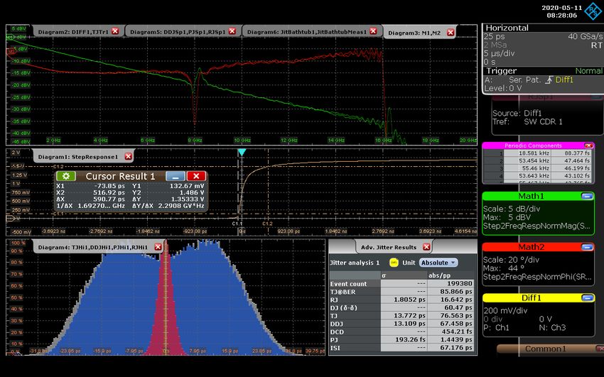
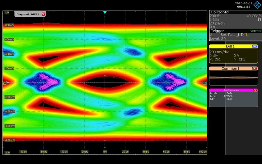
It is important to analyze the jitter in the same way, just as                               The user has the option to configure the step response
the receiver would receive and clock the data. The oscil-                                    length in the estimation; in this case, it is set to 75 UI.
loscope therefore captures the differential TX data and                                      Setting the step response length is governed by three
uses a hardware clock data recovery (CDR) to trigger on                                      principals:
the data signal (see Fig. 1). Notice the high update rate                                    ► The longer the configured step response length, the
(122 000 waveforms/s) of the R&S®RTP high-performance                                           longer the computation time.
oscilloscope.                                                                                ► The step response length should be longer than the
                                                                                                channel memory. A long step response is beneficial for
                                                                                                detailed step response analysis.
                                                                                             ► The run length of the pattern should be longer than the
                                                                                                step response length.

                                                                                             The user can analyze the step response with familiar tools
                                                                                             such as a cursor and automated measurements. In the
                                                                                             example, the rise time is measured via a cursor. The mea-
                                                                                             surement of the rise time tr lets the user estimate the
                                                                                             bandwidth fB of the channel, using the approximation
                                                                                             fB = 0.35 ⁄ tr , which is valid for a single-pole lowpass filter.

                                                                                             More detailed analysis in the frequency domain is there-
                                                                                             fore of interest. Topics such as overshoot, droop and ring-
Fig. 1: Differential eye pattern of a PRBS31 with large ISI.                                 ing of the transfer function are also visible in the frequency
                                                                                             domain.
Prior to the analysis, the acquisition time should be set
to a value that considers the minimum frequency reso-
lution required for the periodic jitter analysis. To accom-
plish a resolution down to 40 kHz, which is in the range
of switched-mode power supplies (SMPS), and a sam-
pling rate of 40 Gsample/s, the record length is set to
2 Msample (= 2 × (sample rate) / (SMPS switching fre-
quency)) and consequently the acquisition time to 50 μs.

The jitter decomposition algorithm analyses the differential
channel as a non-return-to-zero (NRZ) signal. The neces-
sary CDR is configured with a second order phase-locked
loop (PLL) with a bandwidth of 16 MHz.

The jitter decomposition in Fig. 2 shows results in a table                                  Fig. 2: Results for the TJ and RJ spectrum, including a list of periodic components,
and the statistical data as histograms (TJ, RJ, PJ, DDJ 1)),                                 TJ/RJ/PJ/DDJ histograms and the measured and calculated bathtub.
which as expected is dominated by the DDJ. The bathtub
curve of the BER illustrates a good accordance between
the measured and the calculated BER. The novel part in
this decomposition is the estimated step response shown
in the middle of Fig. 2. The step response is the result of
an ideal step applied to the transfer function of the chan-
nel. An uncalibrated test fixture would be inherently part of
this estimation.

1)
     TJ: total jitter, RJ: random jitter, PJ: periodic jitter, DDJ: data dependent jitter.

2
In addition to the histograms and the estimated step As expected, the magnitude shows a frequency depen-
response, Fig. 3 shows the associated transfer function of dent attenuation, mainly caused by dielectric losses. The
the step response in the frequency domain in magnitude skin effect is rather small. The phase shows the dispersion
(see marker M1) and phase (see marker M2). To calculate of the trace. For both traces, every value above 16 GHz
the transfer function in the frequency domain based on a is noise because of the limited channel bandwidth. At
step response, the math menu offers a set of functions [1]: 8.125 GHz, there is an artifact caused by the data rate.
► Step2FreqRespNormMag(,)
► Step2FreqRespNormPhi(,,) This measurement was compared with a VNA measure-
ment. As the PCIe Gen4 ISI board introduces the ISI, the
associated trace was measured (differential) and the trans-
fer function and the scattering parameter differential/dif-
Phase ferential (S21 DD) compared in the frequency domain (see
Fig. 4).
Magnitude
Both measurements show a good accordance in the band
of 0 Hz to 16 GHz. The magnitude deviates less than 1 dB
and the phase less than 5°.
Fig. 3: Step response of the DUT plus test fixture and the transforms for magnitude
and phase.
Fig. 4: Comparison of S21 measured by the VNA and the oscilloscope's transfer function estimate.
0
|S21| in dB
|S21| (VNA)
–5
|S21| (oscilloscope rise)
–10 |S21| (oscilloscope fall)
–15
–20
–25
–30
–35
–40
0 2.5 5 7.5 10 12.5 15
Frequency in GHz
60
S21 phase in °
40
20
0
S21 phase (VNA)
–20
S21 phase (oscilloscope rise)
–40
S21 phase (oscilloscope fall)
–60
–80
–100
–120
0 2.5 5 7.5 10 12.5 15
Frequency in GHz
Rohde & Schwarz Signal integrity analysis for high speed datacom interfaces 3Summary References
The R&S®RTP and R&S®RTO2000 oscilloscopes analyze [1] A. M. Nicolson, “Forming the fast Fourier transform
digital high speed signals for signal integrity. The oscillo- of a step response in time-domain metrology,”
scopes measure precisely well-known jitter components Electronic Letters, Volume 9, Issue 14, p. 317, 1973.
such as TJ, RJ, PJ and DDJ. The oscilloscopes also analyze
inherently the transfer function, which causes the DDJ. A See also
separate characterization of individual components of the www.rohde-schwarz.com/product/sw_rtx-k133
transmission path is challenging due to accessibility, and
the output impedance of the signal driver over frequency
is typically unknown. Therefore, the inherent measurement
of the transfer function is a key element to understand the
sources of the DDJ.
3609040892
The terms HDMI and HDMI High-Definition Multimedia Interface, and the HDMI Logo are trademarks or registered trademarks of HDMI Licensing, LLC in the United States
and other countries.
3609.0408.92 01.00 PDP/PDW 1 en
Rohde & Schwarz GmbH & Co. KG
www.rohde-schwarz.com R&S® is a registered trademark of Rohde & Schwarz GmbH & Co. KG
Trade names are trademarks of the owners
Rohde & Schwarz training PD 3609.0408.92 | Version 01.00 | March 2021 (sk)
www.training.rohde-schwarz.com Signal integrity analysis for high speed datacom interfaces
Rohde & Schwarz customer support Data without tolerance limits is not binding | Subject to change
www.rohde-schwarz.com/support © 2021 Rohde & Schwarz GmbH & Co. KG | 81671 Munich, GermanyYou can also read