Silicon Photonics Prof. Sasan Fathpour
←
→
Page content transcription
If your browser does not render page correctly, please read the page content below
Silicon Photonics
                                Prof. Sasan Fathpour
                                  fathpour@creol.ucf.edu
                                  http://ipes.creol.ucf.edu

                  CREOL, The College of Optics and Photonics
                         University of Central Florida
                             Orlando, FL, 32816

                                     A Short Course at
                          CREOL Industrial Affiliates Symposium
                                      March 6, 2014
                          2:45-3:15 pm, Room 102, CREOL Bldg.
1 Affiliates Day Short Course                                 Sasan Fathpour, CREOL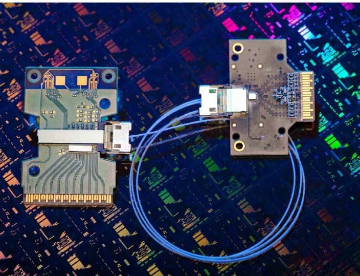
Instructor’s Bio
   2005: Ph.D., University of Michigan, Ann Arbor
   Dissertation on Lasers and Spintronic Light
   Sources Based on III-V Quantum Dots
   Advisor: Pallab Bhattacharya

   2005-2007: Postdoctoral Fellow, UCLA
   Mentor: Bahram Jalali
   2007: Visiting Assistant Professor, UCLA

   2008: Senior Researcher at Ostendo Technologies,
     Carlsbad, CA

   2008-Present: Assistant Professor
   CREOL, The College of Optics and Photonics, UCF
2 Affiliates Day Short Course                 Sasan Fathpour, CREOL
Relevant works by the instructor

                                              Silicon Photonics
                                              B. Jalali and S. Fathpour
                                              IEEE Journal of Lightwave Technology
                                              40th Anniversary Special Issue on
                                              Optoelectronics
                                              vol. 24, pp. 1400–1415, December 2006

  Silicon Photonics for Telecommunications and Biomedicine
  Edited by S. Fathpour and B. Jalali, CRC Press, 2012
                                  Interested in a full course:
                                OSE 6938S: Integrated Photonics
3 Affiliates Day Short Course                                      Sasan Fathpour, CREOL
4 Affiliates Day Short Course Sasan Fathpour, CREOL
Course Outline
Part 1: Introduction and passive silicon photonic devices
Applications
A bit of history
Silicon-on-insulator waveguides, MMI, AWG, etc.
Part 2: Active silicon photonic devices
Light modulation, detection, and emission in silicon
Part 3: Current trends and challenges
Will photonics truly merge with VLSI CMOS?
Competing technologies for silicon photonics
Part 4: Nonlinear silicon photonics
Physics and devices
Contents focused on:
1. Applications 2. New functionalities 3. Instructor’s expertise
5 Affiliates Day Short Course Sasan Fathpour, CREOL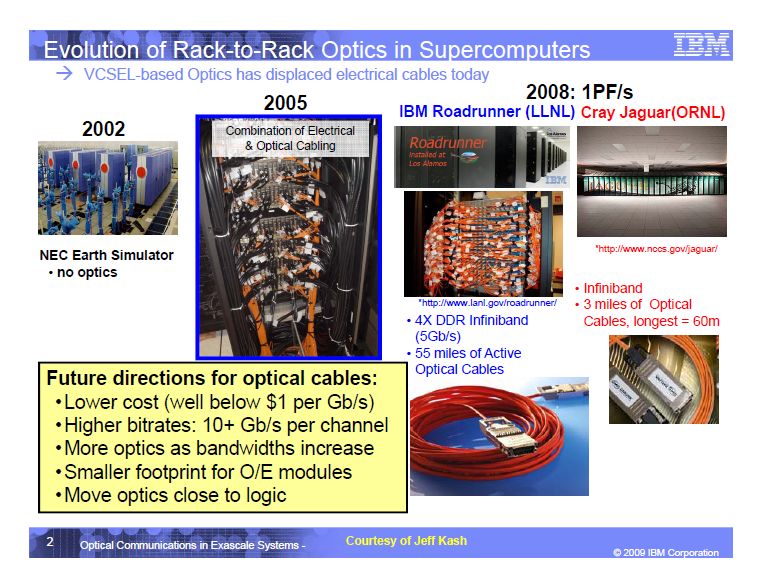
Battle between Optics and Copper
Optical Copper
Chip to Chip
1 – 50 cm
Metro &
Long Haul Optical
0.1 – 80 km Products Billions
Board to Board
Volumes
50 – 100 cm
Rack to Millions
Rack
1 to 100 m
Thousands
Decreasing Distances→
Figure Courtesy of Mario Paniccia, Intel
Drive optics to high volumes and low costs
6 Affiliates Day Short Course Sasan Fathpour, CREOL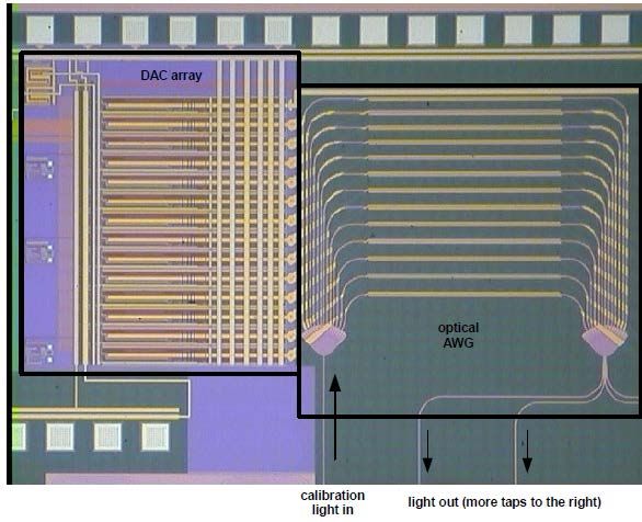
Why Integrated Photonics?
Advantages to discrete photonic components:
More compact
Higher bandwidth
Wavelength multiplexing
Batch fabrication, i.e., cheaper
More reliable
Possibility of integration with electronics
Immunity to mechanical vibrations
Hello!
Bye Bye!
7 Affiliates Day Short Course Sasan Fathpour, CREOL
The Vision for Integrated Photonics or
        Optoelectronic Integrated Circuits
                                Amplifier and/or

                                  Courtesy of Intel Inc.
                     Figure: http://www.tweakers.net/ext/i.dsp/1109883395.png
8 Affiliates Day Short Course                                             Sasan Fathpour, CREOL
Si Photonics: An Industry 25 Years in the Making
        Dr. Richard Soref (USAF) pioneered Si photonics in the ‘80s
                                    “…single-crystal Si will be suitable for building
                                    directional couplers, filters, star couplers, optical
                                    switches, mode converters, polarizers,
                                    interferometers, and modulators that operate at λ
                                    = 1.3 or 1.6 µm (and beyond)-essentially every
                                    integrated-optical component except an optical
                                    source. The use of Si for photodetection at 1.3 µm
                                    has also been suggested.”
        Fundamental work              R. A. Soref and J. P. Lorenzo, J. Quant. Electron. 22, 873 (1986)
        developing silicon
        waveguides between
        1985-1989

        Silicon-based “superchip”
        Proposed by Soref, 1993.

                 n Si
                 n+ Si

9 Affiliates Day Short Course                                              Sasan Fathpour, CREOL
Application 1: Low-Cost Optical Transceivers
                 Transmitter/                     Optical                Receiver/
                   Receiver                       Channel               Transmitter

                                                            10 Gb/s Transceiver - Luxtera

   Wyatt Gibbs, Scientific American, Nov. 2004.
                                                      Key to success: a high volume
   160 Gb/s Transceiver - IBM
                                                                 market
                                                                          Luxtera: 4x10 Gb/s
                                                                          Active Optical Cable

10Affiliates Day Short Course                                              Sasan Fathpour, CREOL
Optical Interconnects for
Data Centers and Supercomputers
Sun Microsystems’s Data IBM’s Supercomputing
Center Technology Technology
11 Affiliates Day Short Course Sasan Fathpour, CREOLHuge market for Active Optical Cable (AOC) 12Affiliates Day Short Course Sasan Fathpour, CREOL
13Affiliates Day Short Course Sasan Fathpour, CREOL
Futuristic Application: Optical Interconnects

                                                                    IEEE Spectrum 2002

                                                  •   D. A. B. Miller, JSTQE 2000
                                                  •   M. Kobrinsky et al., Intel Technology
                                                      Journal, 2004
                                                  •   Wyatt Gibbs, Scientific American 2004
                                                  •   P. Fauchet et al., JSTQE 2006

  Wyatt Gibbs, Scientific American, Nov. 2004.
Affiliates Day Short Course                      14                     Sasan Fathpour, CREOL
Microelectronics in the Last Half a Century
two
transistors Smaller
Smaller
Smaller
Smaller
Texas Instruments
Smaller
Smaller
Smaller
Smaller
Smaller
Smaller
Smaller
Intel’s 62- Core Xeon Phi: Smaller
5 billion transistors Smaller
Smaller
Smaller
15Affiliates Day Short Course
Smaller
Sasan Fathpour, CREOLCelebrated Moore’s Law
Source: Intel
16Affiliates Day Short Course Sasan Fathpour, CREOLWill Silicon Have Steel’s Destiny?
Cleanroom workers, 2005 Steel workers in 1905, Meadville PA
• US steel production increased at an exponential rate from
1860 to 1900.
• In 1900-1950, it increased at a more modest rate.
• Steel remains the principal structural material.
17Affiliates Day Short Course Sasan Fathpour, CREOLCopper Interconnect Limitations
Problems with chips today:
1) Latency
2) Bandwidth
3) Power Dissipation
4) Electromagnetic Pentium 4
Interference
5) Signal Integrity
18Affiliates Day Short Course Sasan Fathpour, CREOLProblem 1: Latency of Global Interconnects
30
Length Aluminum
Interconnect
25 Unlike
metal transistors,
for which
Latency =
20 performance
Resistance x improves with
Capacitance
Delay (ps)
Copper scaling, the
~1/κ2 Interconnect delay of
15
interconnects
increases
10 with scaling
5 Gate
Delay
0
500 350 250 180 130 90 65
Technology Node, κ (nm) Jim Brown et al., CICC 2004
19Affiliates Day Short Course Sasan Fathpour, CREOLOptimal Reverse Scaling
M. J. Kobrinsky et al., Intel Tech. J. 8, 129 (2004)
20Affiliates Day Short Course Sasan Fathpour, CREOLProblem 2: Bandwidth
Need for optical chip-to-chip interconnects:
SONY CELLTM Processor
(Playstation 3)
9 core main processor
256 GFLOPS @ 4GHz
Memory XIO FlexIO Graphics
Processor
26 GB/s 77 GB/s
(max)
http://www.scei.co.jp/corporate/release/pdf/050517e.pdf, FLOPS: floating-point operations per second
http://www.us.playstation.com/pressreleases.aspx?id=252
21Affiliates Day Short Course Sasan Fathpour, CREOL“Sound Barrier” for Silicon?
Clock Speed
Aircraft Speed
David A. Muller,
Nature Materials 5,
645 (2005)
It is an irony that the integrated
circuits’ (IC) clock stopped
increasing the year its inventor,
Jack Kilby, died in 2005!
Affiliates Day Short Course 22 Sasan Fathpour, CREOLProblem 3: Power Dissipation F. J. Pollack, 32nd Annual ACM/IEEE International Symposium on Microarchitecture, Haifa, Israel, 1999. http://sss.lanl.gov/presentations/021003-UIUC.pdf Affiliates Day Short Course 23 Sasan Fathpour, CREOL
Options for Global Interconnects Beyond
the Metal/Dielectric System Ultimate solution:
Use Different Signaling Methods The most potent antidote
– Signal design would be to discover an
– Signal coding techniques interconnect nanotechnology
Use innovative design and package options that provided high-temperature,
– Interconnect-centric design superconductive materials with
– Package intermediated interconnect resistivity → 0
– Chip-package co-design
Use Geometry
– 3D
Use Different Physics
– Photonics (emitters, detectors, free space, waveguides)
– RF/microwaves (transmitters, receivers, free space, waveguides)
– Terahertz photonics
Radical Solutions
– Nanowires/nanotubes
– Molecules
INTERNATIONAL TECHNOLOGY
– Spin ROADMAP FOR SEMICONDUCTORS
– Quantum wave functions 2005 EDITION
24Affiliates Day Short Course Sasan Fathpour, CREOLOptical Interconnects
Optical clocking
Optical
source
interconnect
(IEEE Spectrum, 2002)
Inter-chip Intra-chip
Wavelength Division Multiplexing:
… λ
Optical Receiver
(photodetector/
Local electrical
λ1 λ 2 λ3 λ4 λ5 λn H-tree
TIA) distribution
http://photonics.mit.edu/Optical_Clock.html
25Affiliates Day Short Course Sasan Fathpour, CREOLSpeed of Electrical and Optical Waves
• It is not electrons or other charge carriers that carry the signals in
wires, rather it is electromagnetic waves (of one kind or another)
• Signals in wires do not propagate at the electron velocity ( ~ 106 m/s) but
at light velocity (or somewhat smaller if the cables are filled with a
dielectric)
• However, in electrical interconnection, the signals do move at a slower bit
rate, i.e., the RC delay limits the bandwidth.
David A. Miller, Int. J. Optoelectronics 11, 155-168 (1997)
26Affiliates Day Short Course Sasan Fathpour, CREOLPhotonics is good for silicon but
is silicon good for photonics?
+ Transparent in 1.3-1.6 µm region
+ CMOS compatibility
+ Low cost
+ High-index contrast – small footprint
− High index contrast – high waveguide loss
− No detection in 1.3-1.6 µm region (in bulk Si)
− No linear electro-optic effect
− No efficient light emission
− High cost of state-of-the art CMOS
27Affiliates Day Short Course Sasan Fathpour, CREOLWhy Silicon Photonics?
B. Jalali et al., J. Select. Topics Quant.
Electr. 4, 938 (1998)
Xbox 360 Playstation
SOI: silicon on insulator
Wii
air
n =1
•Compatibility with CMOS electronics on
SOI wafers
• High-refractive index contrast
• sharp bends
• small waveguide cross-sections
28Affiliates Day Short Course Sasan Fathpour, CREOLWafer splitting (SmartCutTM Process to
produce UnibondR wafers)
G. K. Celler and S.
Cristoloveanu, J. Appl. Phys.
93, 4055 (2003)
Implant Dose = 5x1016 cm-2 Developed at LETI,
France in mid 90’s
•A seed wafer, from which a layer of Si will be removed, is oxidized to a desired thickness
followed by hydrogen implantation (The oxide will become the BOX after bonding).
•After implantation, the seed wafer and the handle wafer are carefully cleaned before
bonding in order to eliminate any particle and surface contaminants and to make both
surfaces hydrophilic.
•Abatch of bonded wafer pairs is loaded into a furnace and heated to a temperature of
400–600°C, at which point the wafers split along the hydrogen implanted plane.
•The as-split wafer surface has a mean roughness of a few nanometers.
29Affiliates Day Short Course Sasan Fathpour, CREOL1990’s work on Passive Si Optics
Directional Coupler, 1996 SOI Arrayed Waveguide
Grating WDM, OFC 1997
Gratings 1998
Multimode Interference
Bahram Jalali, UCLA Coupler, 1996
100 nm
30
Affiliates Day Short Course Sasan Fathpour, CREOLChannel vs. Rib SOI waveguides
IBM’s Si wire waveguides with • 1- μm wide rib waveguides
445 nm x 220 nm cross-section:
Minimal propagation losses of 3.6 •Losses are 0.4 dB/cm and
dB/cm for the TE polarization at 0.5 dB/cm for 380-nm and
1.5 μm 200-nm Si film, respectively
Losses per 90º bend are
measured to be 0.086 dB for a
bending radius of 1 μm and as low
as 0.013 dB for a bend radius of
2 μm.
Y. A. Vlasov and S. J. McNab S. Lardenois et al., Opt. Lett.
Opt. Express 12, 1622 (2004) 28, 1150 (2003)
31Affiliates Day Short Course Sasan Fathpour, CREOLCoupling to Si wire waveguides
Single-mode wire waveguide
Single-mode
fiber
~0.3 μm x 0.3 μm
Coupling loss = 20 dB
12.5 μm
Coupling loss = 0.24 dB
10 μm
R = 4.8 μm
2.5 μm
The cross-sectional area of a Si wire waveguide is about 1,000 times less than that of an
optical fiber
Moreover, strong reflective behavior at unmatched connections will degrade dependence
of the coupling efficiency on wavelength because of Fabry-Perot resonances, i.e.,
Fresnel loss
32Affiliates Day Short Course Sasan Fathpour, CREOLCoupling light into waveguides
Conceptually trivial but challenging in practice
A true example of an engineering problem
Problem: the small size (at most a few micron)
cross-sectional dimensions of WGs
Solutions:
lens waveguide waveguide
Prism coupling
End-fire coupling
Optical
waveguide waveguide
fiber
End-butt coupling Grating coupling
Affiliates Day Short Course Sasan Fathpour, CREOLTapered mode size converters
Vertical taper
light in Lateral tapers
Inverted 3D
Non-inverted 3D
light out
Coupling light from an optical fiber into a silicon waveguide is like pouring
water from a fire hose into a straw
Affiliates Day Short Course Sasan Fathpour, CREOLKotura Inc.: Laterally tapered mode converter
Luxtera Corporation: a 2-D grating design or
holographic lens
The so-called holographic lens is a diffractive-optic structure that
mode-matches the fiber with a 0.1 μm2 waveguide with less than 2.5
dB of loss across the C-band (1532-1562 nm)
The lens is constructed at the gate polysilicon step, already present
in the process, depositing and etching it over the transistor silicon
C. Gunn, Photonics Spectra, March 2006
36Affiliates Day Short Course Sasan Fathpour, CREOLNTT and IBM approach: polymer tapers
Polymer: 3 μm x 3 μm
Silicon: 0.3 μm x 0.3 μm
•The tip of the taper has to be extremely
thin. How thin?
•A 200-μm long taper with a 60-nm
wide tip is needed to attain an
acceptable conversion loss of 1 dB.
T. Shoji et al., Electron. Lett. 38, 1669 (2002)
Y. A. Vlasov et al., Opt. Express 11, 2927 (2003)
37Affiliates Day Short Course Sasan Fathpour, CREOLGrating couplers
Image from:
S. Lardenois et al., Opt. Lett. 28, 1150 (2003)
Different diffraction
orders can be
satisfied
Diffracted beams are
generated by output
θ3q coupling of the guided
mode field due to
n3 scattering by the
β n1 beam
Λ
θ2q Design to minimize
n2 diffracted modes!
Affiliates Day Short Course Sasan Fathpour, CREOLDual grating-assisted directional coupling
surface SiON waveguide thickness = 5 μm, n= 1.478
upper SiON layer thickness = 0.15 μm, n = 1.467
Si3N4 waveguide thickness = 0.5 μm, n = 1.97
lower SiON layer thickness = 0.2 μm, n = 1.467
silicon waveguide thickness = 230 nm, n = 3.476
The total coupling loss from a fiber to silicon waveguide
comprises the fiber to SiON waveguide loss (∼ 0.7 dB) plus
SiON to silicon waveguide loss (2.6 dB)
A coupling efficiency of 55% measured.
G. Z. Masanovic et al., Opt. Express 13, 7374 (2005)
39Affiliates Day Short Course Sasan Fathpour, CREOLAdvanced Passive Devices: WDM Components
Need for various integrated devices to perform many functions that can
be categorized as:
1) Amplitude/intensity components:
couplers, splitters, amplifiers, attenuators, reflectors, modulators
2) Phase components:
Phase shifters, phase modulators
3) Polarization components:
Polarizes, polarization splitters, polarization controllers
4) Wavelength components:
Wavelength filters, multiplexers, demultiplexers
5) Frequency components:
Frequency shifters, filters
A lot of these components are
available based on fibers for in-line
6) Active components: fiber optics operation. Is silicon
Lasers, amplifiers photonics ready to compete?
7) Circulators:
Optical isolators, optical circulators
40Affiliates Day Short Course Sasan Fathpour, CREOLWaveguide directional couplers
Pi
incident Pt transmitted
reflected P
r Pc coupled
Coupling ratio R[%] =[Pc/(Pt+Pc )] x 100; R [dB] = -10 x log(R[%])
Excess loss Li[dB] = 10 x log[Pi/(Pt+Pc)]
Insertion loss = 10 x log(Pi/Pc) = R [dB]+ Li
Directivity = 10 x log (Pr/Pi)
Good directional couplers should have
Low insertion loss and high directivity
Commercially available in fibers:
R ~ 50/50 to 1/99
Excess loss < 0.1 dB insertion loss < 3.4 dB
Directivity better than -55 dB
Can integrated devices beat fiber-based devices?
41Affiliates Day Short Course Sasan Fathpour, CREOLMultiplexers/Demultiplexers
Directional couplers are wavelength-
sensitive (look at the theory)
Consider a coupler with κ1, κ2 at λ1 and
λ2, respectively, so that κ1L = mπ and
κ2L = (m-1/2)π
P2(λ1,L) = PixSin2(κ1L) = 0
P2(λ2,L) = PixSin2(κ2L) = Pi
That is a 2x2 demultiplexer
The same device can be used as a
multiplexer (how?)
incident Pi λ1 only
P1
P2
λ2 only
42Affiliates Day Short Course Sasan Fathpour, CREOLMultimode Interference (MMI) splitters
1 x 32 fiber splitter
B. Jalali et al., J. Select. Topics Quant. Electr. 4, 938 (1998)
•The MMI coupler consists of single-mode input and output waveguides separated
by a slab region
•The slab region supports a large number of modes that propagate with different
phase velocities leading to periodic self-imaging
• The output waveguides are placed at the positions of the intensity peaks.
•Thelength of the multimode section scales as L ~ W 2/m, where m is the number
of maxima in the image (or the fanout) and W is the effective WG width
43Affiliates Day Short Course Sasan Fathpour, CREOLMxN Star Couplers
• A star coupler combines the optical signals entering from its multiple
input ports and divide them equally among the output ports
• In contrast to demultiplexers, star couplers do not contain
wavelength-selective elements, as they do not attempt to separate
individual channels
• The number of input and output channels may not be the same
•For example, for video distribution, a relatively small (e.g., 100)
channels may be sent to thousands of subscribers
An 8x8 star coupler formed by using twelve 2x2
single-mode fiber couplers
Integrated M x N Star Coupler
P. D. Trinh et al., Photon. Tech. Lett. 8, 794 (1996)
44Affiliates Day Short Course Sasan Fathpour, CREOLArrayed Waveguide Grating (AWG) or
phased-array (PHASER) Devices
•The WDM signals
experience different
phase shifts due to
different waveguide
lengths
•Moreover, the phase
shifts are wavelength-
dependent because of
λ1,λ2,λ3… λn
the frequency
dependence of the
mode-propagation
λ1 constant
…
Free propagation region
λn •Different channels
focus to different
M. K. Smit and C. van Dam, J. Select. Topics Quant. Electr. 2, 236 (1996) output waveguides
A. Kaneko et al. , J. Select. Topics Quant. Electr. 5, 1227 (1999)
Affiliates Day Short Course 45 Sasan Fathpour, CREOLSilicon Photonics-Based AWG
P. D. Trinh et al., Photon. Tech. Lett. 8, 940 (1997)
Affiliates Day Short Course 46 Sasan Fathpour, CREOLFabry-Perot filters Free spectral range
L FSR or Δλ
Transmission
3dB
n1 n2 WG n2 n1 3dB Bandwidth
δλ
(δλ or FWHM)
λR=2neffL/m
Acts as
a filter
λr,q λr,q-1
input R R output
FSR: Δλ = λr2/(2ngL); ng = neff - λ(dneff/dλ) group index of refraction
FWHM: δλ = λR2 x (1-R)/(2πLng) x (1-R)/√R,
Finesse: F = FSR/FWHM = Δλ/δλ = π√R/(1-R)
Quality Factor: Q = λR/δλ = ngLωR√R/c(1-R)
Large FSR (Δλ) and small FWHM (δλ) are demanded (why?) large F
For today’s DWDM systems, optical filter bandwidths of < 0.8 nm are
desirable, which can be met by integrated FP resonators
However, their FSR is < 10 nm, i.e., multiple channels are passed at the
same time
To achieve 40 nm FSR, < 9 nm cavity lengths are required!!
Affiliates Day Short Course 47 Sasan Fathpour, CREOLRing resonators
•Light is coupled into the ring via
evanescent field of the input WG
(also known as input bus)
λR,m λR,m+1
•The ring is at resonance when the
full trip around the ring is m x 2π,
input through
where m is an integer
•Resonance wavelength:
λR = 2π R neff/m, where R is the ring
radius • At resonance, light coupled
into the ring constructively
• FSR: Δλ = λR2/(2πRng) interferes with the input light
•Assuming weak coupling between the •As a result, optical intensity in
ring and the two waveguides (both the ring can build up and be
represented by κ): significantly higher than the
• FWHM: δλ ≈ κ2 λR2/(4π2 R ng ) waveguide
• F ≈ 2 π/κ2, Q = λR/δλ ≈ 4π2Rng/κ2λR •But of course, light will also
experience loss
Affiliates Day Short Course 48 Sasan Fathpour, CREOLRing resonator filters: MUX/DEMUX
M. Lipson, J. Lightwave Tech.
23, 4222 (2005)
• Finesse, F, defined as Δλ/δλ , while quality factor, Q, defined as λR/δλ
• Alternative way of looking at Q:
•If N is the number of round trips required to reduce optical intensity
to 1/e of the initial value, the finesse is F = 2π x N
• Q = ωRT N = 2πNcT /λR (T: time for trip around the ring)
Affiliates Day Short Course 49 Sasan Fathpour, CREOLBragg Gratings as filters
λin = λ1, λ2, λ3, λ4
λout = λ1, λ3, λ4
grating waveguide
λreflected = λ2
(κ G / α ) 2 sinh 2 (αL) (ω − ω B )neff
R= for < κG
1 + (κ G / α ) 2 sinh 2 (αL) c
α = κ G2 − ϕ 2 , ϕ = kneff − mπ / Λ
At phase-matching condition: λreflected = λB = 2neffΛ/m
FSR = λB (m = 1) - λB (m = 2) = neffΛ
As low as 0.12-nm channel spacing, i.e., FSR demonstrated
Linewidth: Δω = 2κGc/2neff Δλ = λ2κG/(2πneff)
Maximum reflectivity: Rmax = tanh2(κGL)
For a narrowband filter: small κG
For a high-efficiency filter: κGL >> 1
Affiliates Day Short Course 50 Sasan Fathpour, CREOLIntegrated silicon photonic filters
F = 591, Q = 280,000
F = 375, Q = 39,350 FSR = 3.25 nm = 428 GHz
FSR = 0.083 nm = 1.8 THz
Q. Xu et al., Nature 435, 325 (2005)
L. W. Luo et al., Opt. Express 19,
6284 (2011)
M.W. Pruessner et al., LEOS 2006, 46
(2006)
F = 196, Q = 10,774, FSR = 81.7 nm = 8.9 THz, FWHM = 0.15 nm
Affiliates Day Short Course 51 Sasan Fathpour, CREOLCascaded apodized grating waveguides for delay lines
Λ1
L w1 D
Λ2
S. Khan and S. Fathpour:
Optics Letters 38, 3914 (2013)
Optics Express 21, 19538 (2013)
Optics Express 20, 19859 (2012)
Optics Express 19, 11780 (2011)
Demonstration of tunable optical delay
Funded by the National Science lines based on apodized grating
Foundation (NSF) waveguides
Affiliates Day Short Course Sasan Fathpour, CREOL 52Part II: Active silicon photonics
Silicon optical modulators
Optical
Transmitter Receiver
Channel
? ?
Affiliates Day Short Course 53 Sasan Fathpour, CREOLOptical modulation in Si Photonic Circuits
Which effect will work?
Pockels (linear electro-optic) effect
Kerr (second-order electro-optic) effect
Franz-Keldysh effect
Thermo-optic effect
Plasma dispersion effect
54Affiliates Day Short Course Sasan Fathpour, CREOLPockels (linear electro-optic) effect
In a linear electrooptic material, like LiNbO3, the
index ellipsoid is changed in the presence of an applied
electric field, Edc, i.e., ∆n α Edc , via the electrooptic
coefficients rijk
The key for having Pockels effect is using an
anisotropic medium
Silicon has a centrosymmetric lattice structure
All rijk vanish
Si lacks second-order nonlinear effect
Pockels effect is virtually nonexistent in silicon
55Affiliates Day Short Course Sasan Fathpour, CREOLKerr (second-order electro-optic) effect
Kerr effect is related to
third-order optical
nonlinearity (P α X(3)E3)
In Kerr effect, ∆n α Edc2
∆n = s33 n0 Edc2/2
s33 is the Kerr coefficient
n0 is the unperturbed
refractive index
In Si, ∆n ~ 10-4 achieved
for Edc ~ 106 V/cm
The effect is relatively R. Soref and B. Bennett, IEEE J.
small compared to plasma Quantum Electron. 23, 123 (1987)
dispersion effect
56Affiliates Day Short Course Sasan Fathpour, CREOLFranz-Keldysh effect
Edc
hν < Eg d’
e
Franz Keldysh effect:
Electroabsorption due to presence
of a strong electric field
Franz Keldysh effect also induces
electrorefraction
However, the effect diminishes
significantly at telecom wavelengths R. Soref and B. Bennett, IEEE J.
Quantum Electron. 23, 123 (1987)
57Affiliates Day Short Course Sasan Fathpour, CREOLThermo-optic effect
The refractive index changes by applying heat to the
material
In silicon dn/dT = 1.86 x 10⁻⁴ /K
π-shift demonstrated in a 500 μm waveguide with 10 mW
of applied heat
corresponding to ∆T = 7 °C ∆n = 1.3 x 10⁻³
Issues:
Controlling the temperature rise to the locality of the
waveguide
Efficiency of the mechanism used to deliver heat
Warning:
Thermooptic effect: dn/dT > 0
Carrier-plasma effect (next slide): dn/dN < 0
The effects could compete in a poorly designed modulator
58Affiliates Day Short Course Sasan Fathpour, CREOLPlasma dispersion effect
(carrier injection/depletion)
modulating 1 1 0 1
signal
~ Output
P 1 1 0 1
Pump
N
Modulate free-carrier density to modulate optical loss:
α FCA = ∆α e + ∆α h = (8.5 ×10 −18 ⋅ ∆N + 6.0 × 10 −18 ⋅ ∆P)
and/or refractive index:
∆n = ∆ne + ∆nh = −(8.8 × 10− ⋅ ∆N + 8 .5 ×10 − ⋅ ( ∆P ) )
22 18 0.8
59Affiliates Day Short Course Sasan Fathpour, CREOLThe first Si switch (modulator)
8-20 μm
1.5 μm ∆n (N/N+) = 0.015
6 μm
N =7.5x1015 cm-3 L = 0.4-2.0 mm
N+=2.0 x 1019 cm-3
Silicon-based 2 x 2 optical switches
fabricated based on refractive index
change induced by injected minority
carriers
Carrier injection into the mid-section
layer (directional coupler) by forward-
biasing the p+-n junction diode
The phase shift by carrier injection allows
switching into port 3 or 4
J. P. Lorenzo and R. A. Soref, Appl.
Phys. Lett. 51, 6 (1987)
60Affiliates Day Short Course Sasan Fathpour, CREOLIntel’s carrier-depletion 40 Gb/s MZI modulator
Travelling-wave
design allow co-
propagation of
electrical and
optical signals along
the length of the
device
A. Liu et al., Opt. Express 15,
660 (2007)
L. Liao et al., Electr. Lett. 43,
(2007)
61Affiliates Day Short Course Sasan Fathpour, CREOLIntel’s 10 Gb/s MOS-based MZI modulator
• In the accumulation operation, the n-type
silicon in the phase shifter is grounded and
a positive drive voltage, VD, is applied to
the p-type polysilicon.
• When a positive VD is applied to the
device, a thin charge layer is accumulated
on both sides of the gate oxide
A. Liu et al., Nature 427, 615 (2004)
L. Liao et al., Opt. Express 13, 3129 (2005)
62Affiliates Day Short Course Sasan Fathpour, CREOLRing-resonator modulators
Carrier injection via a p-n
junction n into a ring resonator
shifts its resonance, leading to a
modulation effect
Used:
BOX thickness: 3 μm
Waveguide: 450 nm x 250 nm
ring diameter: 12 μm Q. Xu et al., Nature 435, 325 (2005)
spacing between the ring and the
straight waveguide: 200 nm
63Affiliates Day Short Course Sasan Fathpour, CREOLPart II: Active silicon photonics
Photodetectors
Affiliates Day Short Course 64 Sasan Fathpour, CREOLAbsorption coefficient
α (ω ) = (ω − E g ,Si )2
α (ω ) = (ω − E g ,GaAs )1/ 2
Direct vs. indirect bandgap materials
65Affiliates Day Short Course Sasan Fathpour, CREOLSi Photodetectors
Photodetectors are perhaps the oldest and best
understood silicon photonic devices.
Commercial products operate at wavelengths below
1000 nm, where band-to-band absorption occurs.
Additionally, used in conjunction with scintillators,
they are widely used as X-ray detectors that are used
in medical computed tomography equipment and airport
luggage scanners.
For application in fiber-optic communication, silicon is
not the right material since it is transparent in the
1300- and 1550-nm operating wavelengths of these
networks.
66Affiliates Day Short Course Sasan Fathpour, CREOLSiGe Photodetectors
Strain limits the thickness of Ge layers that can be
epitaxially grown on silicon.
A thin Ge layer is preferred from the bandwidth
point of view as it minimizes the carrier transit time,
but it comes at the expense of reduced absorption
and diminished responsivity.
A waveguide p-i-n geometry is preferred over a
normal-incidence design since it allows independent
optimization of absorption volume and transit time.
Incident light
Ge
SiGe or Ge? Si
SiO2
Si Si
67Affiliates Day Short Course Sasan Fathpour, CREOLGe-on-Si Vertical Incidence Photodiodes
with 39-GHz Bandwidth (Univ. of Stuttgart)
M. Jutzi et al., Photon. Tech. Lett. 17, 1512 (2005)
The detector comprises a 300-nm-thick intrinsic region, and
exhibits zero bias external quantum efficiencies of 23%,
16%, and 2.8% at 850, 1298, and 1552 nm, respectively.
68Affiliates Day Short Course Sasan Fathpour, CREOLA 15-Gb/s 2.4-V Optical Receiver Using
a Ge-on-SOI Photodiode and a CMOS IC
L. Colace et al., Appl. Phys. Lett. 88, 101111 (2006)
λ =850 nm
Affiliates Day Short Course Sasan Fathpour, CREOLIntel’s 40 Gb/s waveguide photodetectors T. Yin et al., Optics Express 15, 13965 (2007) 70Affiliates Day Short Course Sasan Fathpour, CREOL
Part II: Active silicon photonics

                                Light emission in silicon

71Affiliates Day Short Course                               Sasan Fathpour, CREOL
Silicon Lasers:
If only Silicon Were a Direct Band-Gap Material!
GaAs Phonon-mediated Silicon
Energy
transition
or InP
Momentum
Light Light
(photon) (photon)
Direct bandgap Indirect bandgap
III-V semiconductor silicon
First order transition: very efficient 2nd order transition: ~ 1000x less efficient
72Affiliates Day Short Course Sasan Fathpour, CREOLWhy Silicon Cannot Amplify Light
4
10 4
10
(cm-1-1))
Free-Carrier
(cm
GaAs n
bso
rptio Absorption
gain/loss
r a
rrie
Optical Gain
2
10 2
10
re e ca Si
F
Optical
0
gain in GaAs
10 0
10 gain in Si
FCA
18 19 20 21
1018 10 19 10 20 1021
10 10 10-3
10
Electron density (cm )
Electron Density (cm-3)
♦ Gain in silicon is lower because of indirect bandgap
♦ Free-Carrier Absorption prevents silicon from achieving gain
♦ Auger recombination becomes significant at N > 1019 cm-3
♦ Ge is better: less indirect and lower free carrier absorption rate
B. Jalali et al., “Silicon Lasers”, in Silicon Photonics – State of the Art,
edited by Graham Reed, John Wiley, 2007.
B. Jalali, “Making Silicon Lase”, Scientific American, February 2007
73Affiliates Day Short Course Sasan Fathpour, CREOLLight Generation/Amplification Techniques in Si:
Series 1
Erbium-doped Si
Quantum Si rich oxide or Si nanocrystals (NCs)
Confinement • Er-doped Si NCs
and Er-doping Deposition of boron dopant with SiO2
Excellent nanoparticles mix on Si
Review articles:
(M. J. Chen et al., Appl. Phys. Lett. 12, 2163, 2004)
P. Fauchet,
Optical Materials, Dislocation loops
2005
(W. L. Ng et al., Nature 410, 192, 2001)
L. Pavesi,
Materials Today, Surface texturing
2005
(M. A. Green et al., Nature 412, 805, 2001)
Band-engineered Ge-on-Si
using tensile strain and n-type doping
(J. Liu et al., Optics Letters 35, 679, 2010)
74Affiliates Day Short Course Sasan Fathpour, CREOLLight Generation/Amplification Techniques in Si:
Series 2
Bonded III-V on Silicon – UCSB/Intel
Monolithic III-V on Silicon - Univ. of Michigan
Using nonlinear interactions, i.e., Raman laser (Part IV)
Review articles:
B. Jalali and S. Fathpour, J. Lightwave Tech. 24, 4600 (2006)
B. Jalali, “Making Silicon Lase” Scientific American, Feb. 2007
75Affiliates Day Short Course Sasan Fathpour, CREOLBowers et al. UCSB
Paniccia et al. Intel
Startup company: Aurrion LLC (aurrion.com)
Santa Barbara, CA
76Affiliates Day Short Course Sasan Fathpour, CREOLMonolithic III-V on Silicon: Univ. of Michigan
Pallab Bhattacharya et al.
77Affiliates Day Short Course Sasan Fathpour, CREOLPart III:
State of the Industry
and Challenges
78Affiliates Day Short Course Sasan Fathpour, CREOLAcquired
by
Mellanox
79Affiliates Day Short Course
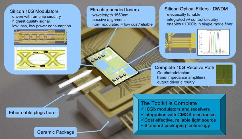
79 Sasan Fathpour, CREOLLuxtera’s 4 x 10 Gb/s Si Transceivers
Top view of a flip-chipped laser on top of a
CMOS die. The laser die is outlined by the
dashed white lines.
A. Huang et al., 2006 ISSCC
Germanium photodetector integrated into
CMOS, shown with 10-Gbps eye
80Affiliates Day Short Course Sasan Fathpour, CREOLIntel’s 4 x 12.5 Gb/s Silicon Photonics Link
InP laser evanescently
coupled into a Si WG
transmitter
receiver
White Paper, Intel Labs, July 2010
W. Fang et al., Opt. Express 14, 9203-9210 (2006)
81Affiliates Day Short Course Sasan Fathpour, CREOLConstituents of CMOS Compatibility
Optical
interconnect
(IEEE Spectrum, 2002)
Material Compatibility
Is silicon
Process Compatibility
photonic truly
Economic Compatibility CMOS
Heat Compatibility compatible?
82Affiliates Day Short Course Sasan Fathpour, CREOLOptical vs. Copper Interconnects
Figure of merit: Bandwidth density/latency
Diffraction
limit
~λ/3 ~ 200 nm
M. Kobrinsky et al., Intel Technology Journal 8, 192 (2004)
WDM signaling is necessary for optical interconnects
to be competitive
83Affiliates Day Short Course Sasan Fathpour, CREOLSide Note: SIMOX 3-D Sculpting in Si
UCLA
OFC 2006
Oxygen Implant
SiO2
Silicon
P. Koonath et al., J.
silicon Lightwave Technol. 24,
oxide 1796 (2006)
silicon
oxide
silicon
84Affiliates Day Short Course Sasan Fathpour, CREOLTwo-Photon and Free-Carrier Absorptions
Free-
Carrier
Scattering
Two-photon Absorption
B. Jalali, Nature Photonics 1, 193 (2007)
linear TPA FCA
85Affiliates Day Short Course Sasan Fathpour, CREOLTwo-photon vs. Conventional Photovoltaic Effect
+ V>0 – p
i
ISubstrate materials used for optical
integrated circuits (OIC)
PASSIVE (incapable of ACTIVE (capable of light
light generation) generation)
Quartz Gallium Arsenide
Lithium niobate AlGaAs, InGaAs,…
Lithium tantalate Indium Phosphate
Tantalum pentoxide InGaP, AlGaP, InGaAsP,…
Niobium pentoxide Other III-V and also II-
Silicon VI semiconductors
Polymers
Affiliates Day Short Course 87 Sasan Fathpour, CREOLIII-V optoelectronic integrated circuits
Pursued since 1980s to monolithically integrate lasers, photodetectors
and the driver/detection electronic circuits on the same GaAs or InP
chip:
OEIC = few channels x (one LD or PD + few transistors)
Nowadays, more and more optical functions are integrated
Generally, integration of LDs with drivers is more complicated than
photoreceivers:
More stringent materials and processing requirements
Affiliates Day Short Course 88 Sasan Fathpour, CREOLTwo early integrated photoreceivers
FET
PD
Fujitsu
Early monolithically integrated
photoreceivers used one-
transistor amplifiers and dealt
mostly with the challenge of
differences between PD vs.
transistor heterostructures
University of Michigan
S. Miura et al., Appl. Phys. Lett. 48, 1461 (1986)
R. Lai et al., Electron. Lett. 27, 364 (1991)
89Affiliates Day Short Course Sasan Fathpour, CREOLAn early integrated transmitter circuit by Fujitsu
Q2 and Q3: differential amplifier to
modulate the laser
Q1: laser bias current controller
Q4: current limiter
S. Yamakoshi et al., Electr. Lett. 19, 1020 (1983)
T. Sanada et al., Appl. Phys. Lett. 46, 226 (1985)
90Affiliates Day Short Course Sasan Fathpour, CREOLAn Early VCSEL Array Flip-Chip Bonded
to Gb/s CMOS Circuits by Bell Labs
• Exposed flip-chip bonding pads on the CMOS
chip were first metallized with Ti–Ni–Au metals
to improve adhesion to the top-level Al on the
chip.
• PbSn (lead-tin) solder was then deposited on
the CMOS chip.
• Next, the bottom-emitting VCSEL array on the
GaAs chip was flip-chip bonded directly over the
CMOS circuits using two coplanar Au contacts
per laser.
• Epoxy was wicked in-between the chips to act
as an adhesive.
•The simple two-transistor VCSEL driver was
based on a current-shunting principle
• A PMOS transistor was used to source an
adjustable amount of current through the laser,
and an NMOS transistor was used to quickly
shunt the current into and out of the VCSEL.
A. V. Krishnamoorthy et al., IEEE Photo. Tech. Lett. 11, 128 (1999)
91Affiliates Day Short Course Sasan Fathpour, CREOLIBM’s CMOS-Based Parallel Optical Transceiver
Capable of 240-Gb/s Bidirectional Data Rates
SLC: surface laminar
circuit carrier
• The “Optochip”, which is comprised of VCSEL and photodiode (PD) arrays that are flip-
chip bonded to a CMOS IC, is directly soldered to a high-density organic chip carrier to form
an optical module, or “Optomodule”.
• The “Optomodule” is then soldered to an underlying circuit board, or “Optocard”, that
contains dense arrays of polymer optical waveguides, 45° turning mirrors, and lenses for
efficient optical coupling.
C. L. Schow et al., J. Lightwave Tech. 27, 915 (2009)
92Affiliates Day Short Course Sasan Fathpour, CREOLInP-based Photonic Integrated Circuits (PIC)
DML: Directly modulated lasers
SOA: Semiconductor optical amplifier
EML: Electroabsorption modulated lasers
R. Nagarajan et al., J. Select. Topics Quant. Electr. 11, 50 (2005)
D. Welch et al., J. Lightwave Tech. 24, 4674 (2006)
93Affiliates Day Short Course Sasan Fathpour, CREOLOneChip Photonics Inc.’s transceiver for fiber-
to-the-home (FTTH) applications
SSC: spot-size converter http://www.onechipphotonics.com/
OneChip Diplexer PIC integrates a number of photonic devices. Images courtesy
of OneChip Photonics Inc.
Monolithic
PIC device
mounted on the silicon
optical bench (SiOB)
provides the heart of the
bidirectional optical
subarray (BOSA), which
is then integrated with
the transceiver printed
circuit board and housing
to form the complete
transceiver configuration
94Affiliates Day Short Course Sasan Fathpour, CREOLInfinera Corporation’s Large-Scale
Photonic Integrated Circuit (LS PIC)
The first commercially
deployed monolithic large-
scale PICs providing transmit
and receive functions
The transmitter (TX) PIC
includes over 50 discrete
functions integrated
monolithically on a single
chip, spread over ten
channels with an aggregate
data capacity of 100 Gb/s.
VOA: Variable optical attenuator A similar monolithic receiver
EAM: electroabsorption modulator
OPM: optical power monitoring
(RX) PIC (not shown here)
AWG: Arrayed waveguide grating supports a similar aggregate
data rate of 100 Gb/s
95Affiliates Day Short Course Sasan Fathpour, CREOLFinal Remark on Heterogeneous Optoelectronics
It appears that for the foreseeable future, hybrid
technologies, that combine group IV and III-V
semiconductor materials, and perhaps LiNbO3 will most
likely dominate integrated optoelectronics:
Electronics will most likely be on Si
Lasers will most likely on be III-Vs
Detectors will more likely be on Ge, but perhaps on
III-Vs
Modulators could be on either Si, III-Vs or LiNbO3
Passive devices (waveguides, filters, etc.) will more
likely be on Si but maybe on III-Vs or LiNbO3
96Affiliates Day Short Course Sasan Fathpour, CREOLTomorrow’s Talk: Silicon photonics beyond SOI
Si III-V
Si Si
III-V
SiO2 III-V Ge Sapphire SiN
Silicon Silicon Silicon
Near-IR silicon photonics Mid-IR silicon photonics
(~1 to ~3 µm) (~3 to ~8 µm)
LiNbO3
Si
SiO2 Si air Si Si
Silicon Silicon LiNbO3
Affiliates Day Short Course Sasan Fathpour, CREOLYou can also read