Ultralow-loss silicon nitride waveguides for nonlinear optics - Zhichao Ye - Photonics Laboratory
←
→
Page content transcription
If your browser does not render page correctly, please read the page content below
T HESIS FOR THE D EGREE OF D OCTOR OF P HILOSOPHY

Ultralow-loss silicon nitride waveguides for
              nonlinear optics

                      Zhichao Ye

                   Photonics Laboratory
   Department of Microtechnology and Nanoscience (MC2)
        C HALMERS U NIVERSITY OF T ECHNOLOGY
                 Gothenburg, Sweden, 2021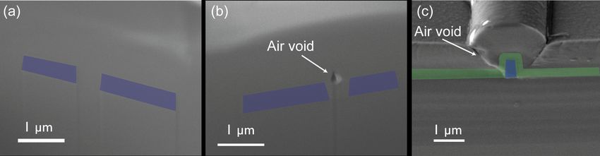
Ultralow-loss silicon nitride waveguides for nonlinear optics

Zhichao Ye

© Zhichao Ye, 2021

ISBN 978-91-7905-458-8
Doktorsavhandlingar vid Chalmers tekniska högskola, Ny series nr 4925
ISSN 0346-718X
Chalmers University of Technology
Department of Microtechnology and Nanoscience
Photonics Laboratory
SE-412 96 Göteborg
Sweden
Telephone: +46 (0)31-772 10 00

Front cover illustration: The schematic illustration of a dark pulse
microcomb, a bright soliton microcomb and a parametric amplifier based on
microring resonators and a spiral waveguide. The colors of the waveguides
indicate the group velocity dispersion.

Printed by Chalmers digitaltryck, Chalmers tekniska högskola, Sweden,
2021
Ultralow-loss silicon nitride waveguides
                      for nonlinear optics
                               Zhichao Ye
                           Photonics Laboratory
              Department of Microtechnology and Nanoscience
                    Chalmers University of Technology
Abstract
The field of nonlinear optics relies on the interaction between high-intensity
optical waves and nonlinear media. An integrated waveguide with large re-
fractive index contrast allows to highly confine optical waves in a sub-µm2
area, thus enhancing the optical intensity. However, such a high optical
confinement increases the susceptibility to scattering losses induced from
nanometer-level inhomogeneities.
Silicon nitride is a dielectric material featuring a relatively large nonlinear-
index coefficient and a broadband transparency window, from ultraviolet to
mid-infrared. Its refractive index contrast to silica allows high confinement
and controlling the dispersion with the waveguide geometry. This material
platform has emerged in the past years as a workhorse for nonlinear optics
applications that rely on the Kerr effect, from microcomb generation to para-
metric amplification. In this thesis work, we focused on the development
of advanced manufacturing techniques for the realization of ultralow-loss
silicon nitride waveguides. Meter long high-confinement waveguides with
record low losses in the order of 1.4 dB/m and dispersion-engineered mi-
croresonators with quality factors of 19 million are reported. Based on this
technology, we demonstrated octave-spanning coherent microcombs and mi-
crocombs with photodetectable repetition rates occupying a device area less
than 1 mm2 , i.e., one order of magnitude smaller than state of the art. The
high yield and ultralow-loss Si3 N4 waveguides also allowed us to achieve,
for the first time, continuous-wave parametric amplification in an integrated
waveguide, with a demonstrated gain of 9.5 dB and noise figure of 1.2 dB
when operated in phase-sensitive mode.

Keywords: silicon nitride, ultralow loss, integrated waveguide, Kerr nonlinear op-
tics, DKS microcombs, parametric amplifiers

                                        i
ii
Acknowledgment

First I would like to thank my supervisor, Associate Prof. Victor Torres-Company,
without his talented leadership, solid supports and fruitful discussions I would not
have made it this far. I also would like to thank my examiner and co-supervisor,
Prof. Peter Andrekson for giving me opportunity to pursue the research work in the
photonics laboratory and providing a challenging but achievable research goal which
motivated me through the past five years.
I would like to thank Dr. Morten Bache and Simon Christensen from DTU for the
collaboration. I also thank Prof. Andrew Weiner, Prof. Minghao Qi, Dr Cong Wang
and Dr. Mohammed Alshaykh from Purdue university for the collaboration.
I would like to acknowledge all the staffs at the nanofabrication laboratory, with-
out their hard work to keep the cleanroom operational I would not have made such
ultralow-loss silicon nitride waveguides. Especially, I would like to thank Dr. Mar-
cus Rommel for teaching me EBL and providing supports for Beamer flows. I also
thank Johan Karl Andersson for his best efforts on maintaining LPCVD furnaces op-
erational.
Moreover, I would like to thank all the members in the photonics laboratory at
Chalmers for both technical and non-technical supports. I would like to acknowl-
edge Dr. Clemens Krückel for developing the initial nanofabrication processes and
teaching me professional cleanroom skills. Dr. Attila Fülöp deserves acknowledg-
ment for spending so much time teaching me microcomb experiments and help me
program equipment. I appreciate Óskar Bjarki Helgason for fruitful discussion about
nonlinear optics and endless talk on everything. I have to thank my office mates
gratefully. Kovendhan Vijayan and Dr. Ravikiran Kakarla for discussions and play-
ing table tennis, Dr. Xiaonan Hu for being my first Chinese colleague and having
discussion both on and beyond research work, Marcello Girardi for creating nice

                                        iii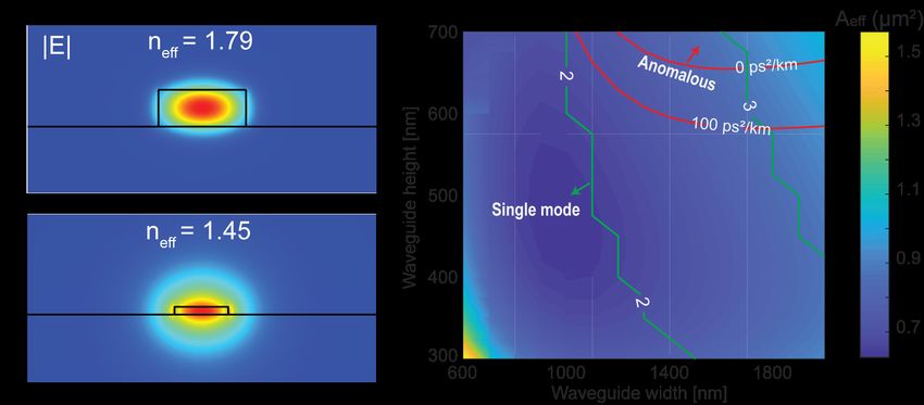
working environment and making work more enjoyable. I would like to thank Dr.
Fuchuan Lei and Dr. Ping Zhao for sharing both enriched knowledge about physics
and funny stories about physicists.
I spent so much time in the cleanroom to optimize the processes. I would like to
thank Dr. Michael Alexander Bergmann for being my lab buddy, having nice discus-
sions when waiting for processes and showing his nice UV LED devices.
I gratefully appreciate Prof. Yaocheng Shi from Zhejiang university, without his
support and encouragement I would not have come to Sweden for both my master
program and PhD work. It turns out to be a good decision.
Last but not least, I would like to thank my family and friends for supports. Es-
pecially, I appreciate my girlfriend Jingwen Zhang for her support, company and
encouragement throughout the years.

                                                                    Zhichao Ye
                                                        Gothenburg, March 2021

                                       iv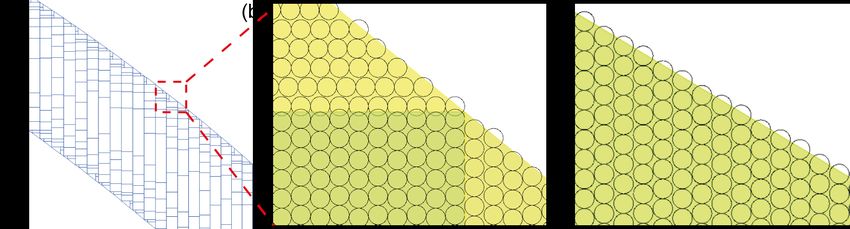
Abbreviations

BSS Beam step size
CMOS Complementary metal-oxide-semiconductor
CVD Chemical vapor deposition
CW Continuous-wave
DCS Dichlorosilane
DFB Distributed feedback
DKS Dissipative Kerr soliton
DUV Deep ultraviolet
EBL Electron beam lithography
FCA Free carrier absorption
FSR Free spectral range
FWM Four-wave mixing
ICP RIE Inductively-coupled-plasma reactive-ion etching
LPCVD Low pressure chemical vapor deposition
NF Noise figure
OFDR Optical frequency-domain reflectometry
OPA Optical parametric amplification
PECVD Plasma-enhanced chemical vapor deposition
PIC Photonic integrated circuit
RMS Root mean square
SCG Supercontinuum generation
SEM Scanning electron microscopy
SiRN Silicon-rich silicon nitride
TEOS Tetraethyl orthosilicate
TPA Two-photon absorption

                                      v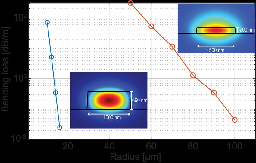
VLSI Very large scale integration

                                    vi
List of papers

This thesis is based on the following appended papers:

 [Paper A] Zhichao Ye, Attila Fülöp, Óskar Bjarki Helgason, Peter A. Andrekson,
           and Victor Torres-Company, "Low-loss high-Q silicon-rich silicon ni-
           tride microresonators for Kerr nonlinear optics", Opt. Lett, vol. 44, no.
           13, pp. 3326-3329 (2019).

 [Paper B] Zhichao Ye, Krishna Twayana, Peter A. Andrekson, and Victor Torres-
           Company, "High-Q Si3 N4 microresonators based on a subtractive pro-
           cessing for Kerr nonlinear optics", Opt. Express, vol. 27, no. 24, pp.
           35719-35727 (2019).

 [Paper C] Simon Christensen, Zhichao Ye, Morten Bache, and Victor Torres-Company,
           "Octave-spanning frequency comb generation in all-normal-dispersion
           silicon-rich silicon nitride waveguide", in Conference on Lasers and
           Electro-Optics (CLEO), San jose, USA, paper. STu3H.7, May 2020.

 [Paper D] Zhichao Ye, Ping Zhao, Krishna Twayana, Magnus Karlsson, Victor
           Torres-Company, and Peter A. Andrekson, "Low-noise continuous-wave-
           pumped parametric amplifier using a silicon-nitride waveguide", Manuscript
           submitted, 2021.

 [Paper E] Zhichao Ye, Fuchuan Lei, Krishna Twayana, Marcello Girardi, Peter
           A. Andrekson, and Victor Torres-Company, "Integrated, ultra-compact
           high-Q silicon nitride microresonators for low-repetition-rate soliton mi-
           crocombs", Manuscript submitted, 2021.

                                        vii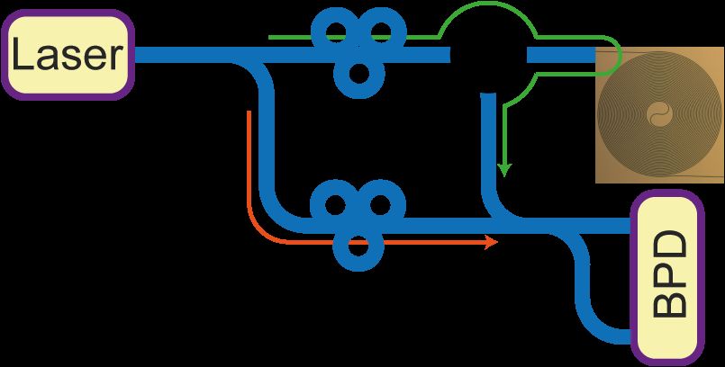
[Paper F] Mohammed S. Alshaykh, Cong Wang, Nathan P. O’Malley, Zhichao
          Ye, Abdullah Al Noman, Daniel E. Leaird, Minghao Qi, Victor Torres-
          Company, and Andrew M. Weiner, "Optical Dual-Comb Vernier Divi-
          sion of an Octave-Spanning Kerr Microcomb", To be presented at CLEO
          2021.

                                   viii
Related publications and conference contributions by the author:
Journal papers:
[Paper G] Clemens J. Krückel, Attila Fülöp, Zhichao Ye, Peter A. Andrekson, and
Victor Torres-Company, "Optical bandgap engineering in nonlinear sili-
con nitride waveguides," Opt. Express 25, 15370-15380 (2017).
[Paper H] Xiaonan Hu, Marcello Girardi, Zhichao Ye, Pascual Muñoz, Anders
Larsson, and Victor Torres-Company, "Si3 N4 photonic integration plat-
form at 1 µm for optical interconnects," Opt. Express 28, 13019-13031
(2020).
[Paper I] Ping Zhao, Zhichao Ye, Kovendhan Vijayan, Corentin Naveau, Jochen
Schröder, Magnus Karlsson, and Peter A. Andrekson, "Waveguide taper-
ing for improved parametric amplification in integrated nonlinear Si3 N4
waveguides," Opt. Express 28, 23467-23477 (2020).
[Paper J] Óskar B. Helgason, Francisco R. Arteaga-Sierra, Zhichao Ye, Krishna
Twayana, Peter A. Andrekson, Magnus Karlsson, Jochen Schröder and
Victor Torres-Company, "Disspative solitons in photonic molecules",
Nature Photonics 2021, https://doi.org/10.1038/s41566-020-00757-9.
[Paper K] Fuchuan Lei, Zhichao Ye, Attila Fülöp and Victor Torres-Company,
"Fundamental optical linewidth of soliton microcombs", arXiv:2102.05517.
Conference presentations and papers
[Paper L] Victor Torres-Company, Zhichao, Attila Fülöp, Clemens J. Krückel, and
Peter A. Andrekson, "High-confinement high-Q silicon-rich silicon ni-
tride nonlinear microresonators," in Advanced Photonics 2018, paper
ITh2J.2.
[Paper M] Luis A. Bru, Zhichao Ye, Daniel Pastor, Pascual Muñoz, "Multi-parameter
estimation of high-Q silicon rich nitride resonators using optical fre-
quency domain reflectometry" Proc. SPIE, vol. 10535, pp. 1053518.
2018.
ix[Paper N] Zhichao Ye, Attila Fülöp, Óskar Bjarki Helgason, Peter A. Andrekson,
and Victor Torres-Company, "Low Loss Silicon-Rich Silicon Nitride for
Nonlinear Optics," in Conference on Lasers and Electro-Optics (CLEO),
San Jose, USA, paper. STu3F.1. May 2018.
[Paper O] Xiaonan Hu, Zhichao Ye, Marcello Girardi, Pascual Muñoz, Anders
Larsson, and Victor Torres-Company, "Passive SiN Photonic Integrated
Platform at 1µm for Short-Range Optical Interconnects," 2019 Confer-
ence on Lasers and Electro-Optics(CLEO) Europe, Munich, Germany,
pp. 1-1, June 2019.
[Paper P] Óskar B. Helgason, Zhichao Ye, Krishna Twayana, Peter A. Andrekson,
Jochen Schroder and Victor Torres-Company, "Dark-pulse Kerr combs
in linearly coupled microring structures," in Conference on Lasers and
Electro-Optics (CLEO), San jose, USA, paper. STu3H.5, May 2020.
[Paper Q] D. Kong, A. A. Jørgensen, M. R. Henriksen, F. Klejs, Z. Ye, Ò. B. Hel-
gason, H. E. Hansen, H. Hu, M. Yankov, S. Forchhammer, P. Andrek-
son, A. Larsson, M. Karlsson, J. Schröder, Y. Sasaki, K. Aikawa, J.W.
Thomsen, T. Morioka, M. Galili, V. Torres-Company, and L. K. Oxen-
løwe, "Single Dark-Pulse Kerr Comb Supporting 1.84 Pbit/s Transmis-
sion over 37-Core Fiber," in Conference on Lasers and Electro-Optics
(CLEO), San jose, USA, Post Deadline paper. JTh4A.7, May 2020.
[Paper R] Zhichao Ye, Fuchuan Lei, Krishna Twayana, Marcello Girardi, Peter A.
Andrekson, and Victor Torres-Company, "25 GHz soliton microcombs
in high-Q Si3 N4 racetrack-shaped microresonators," in Conference on
Lasers and Electro-Optics(CLEO), San jose, USA, paper. JTh2F.29,
May 2020.
[Paper S] Zhichao Ye, Krishna Twayana, Peter A. Andrekson, and Victor Torres-
Company, "High-Q Dispersion-Engineered Si3 N4 Microresonators Based
on a Subtractive Processing Technique," in Conference on Lasers and
Electro-Optics(CLEO), San jose, USA, paper. JTh2F.24, May 2020.
xContents
Abstract i
Acknowledgment iii
Abbreviations v
List of papers vii
1 Introduction 1
1.1 Historical overview . . . . . . . . . . . . . . . . . . . . . . . . . . 1
1.2 This thesis . . . . . . . . . . . . . . . . . . . . . . . . . . . . . . . 6
2 Optical waveguide characteristics 9
2.1 Optical confinement . . . . . . . . . . . . . . . . . . . . . . . . . . 9
2.2 Dispersion engineering . . . . . . . . . . . . . . . . . . . . . . . . 11
3 Waveguide losses 15
3.1 Origin of waveguide losses . . . . . . . . . . . . . . . . . . . . . . 15
3.1.1 Bending losses . . . . . . . . . . . . . . . . . . . . . . . . 15
3.1.2 Design imperfections . . . . . . . . . . . . . . . . . . . . . 16
3.1.3 Mode coupling due to interfacial inhomogeneities . . . . . . 19
3.1.4 Material losses . . . . . . . . . . . . . . . . . . . . . . . . 24
3.2 Waveguide loss characterization methods . . . . . . . . . . . . . . 25
3.2.1 Cut-back method . . . . . . . . . . . . . . . . . . . . . . . 25
3.2.2 Microring resonator . . . . . . . . . . . . . . . . . . . . . 26
3.2.3 Optical frequency-domain reflectometry . . . . . . . . . . . 29
xi4 Effect of linear losses in Kerr nonlinear optics 31
4.1 Kerr effect . . . . . . . . . . . . . . . . . . . . . . . . . . . . . . . 31
4.2 Effect of loss on parametric amplifiers . . . . . . . . . . . . . . . . 33
4.3 Effect of loss on Kerr microcombs . . . . . . . . . . . . . . . . . . 37
5 Fabrication techniques of ultra-low-loss silicon nitride waveguides 41
5.1 Overview of fabrication process . . . . . . . . . . . . . . . . . . . 41
5.2 Silicon nitride thin film deposition . . . . . . . . . . . . . . . . . . 43
5.3 Electron beam lithography . . . . . . . . . . . . . . . . . . . . . . 45
5.3.1 Within a writing field . . . . . . . . . . . . . . . . . . . . . 46
5.3.2 Between writing fields . . . . . . . . . . . . . . . . . . . . 48
5.4 Inductively-coupled-plasma reactive-ion etching . . . . . . . . . . . 49
5.5 SiO2 cladding deposition . . . . . . . . . . . . . . . . . . . . . . . 51
5.6 Analysis of fabrication yield . . . . . . . . . . . . . . . . . . . . . 54
6 Summary and future outlook 57
7 Summary of papers 59
Appendices 63
Papers A–F 85
xiiChapter 1
Introduction
1.1 Historical overview
Before the 18th century, the limited industrial power and transportation engine relied
on animal and human muscle, wind and river. Long-haul traveling and communi-
cation were limited, and continents were quite isolated. Since the first and second
industrial revolution, the unprecedented boost of machine engine enabled fast and
convenient traveling between countries and continents, and new ideas spread quickly.
Later on, thanks to the invention of telephone and the success of optical fiber commu-
nication, people from all over the world became fully connected. The globe turned
into a small village.
A similar evolution happened in electrical circuits. The first transistor was invented
by J. Bardeen, W. Brattain and W. Shockley at Bell labs, and they shared the 1956 No-
bel Prize in Physics for their achievement. The early transistors were large, and long
wires were needed to connect different components. For a computer with complex
microelectric circuits, these wires can significantly slow the computer. The invention
of the integrated circuit by J. Kilby and R. Noyce solved this problem by integrating
all the functional components on a single-crystal Si wafer. It is worth mentioning
that Jack Kilby also got the Nobel Prize in Physics in 2000 for this achievement. The
past 50 years have witnessed a steady development of integrated circuits following
Moore’s law. It is remarkable that the increasing number of transistors in a densely
integrated circuit is encompassed with a significant reduction in computer volume:
1Chapter 1. Introduction
from the size of an entire room to a light and portable device.
The techniques that have been developed for the manufacturing of microelectronic
circuitry (e.g. lithography, etching, film deposition) can be used to manufacture
photonic integrated circuits. PICs have a dominant application in the field of high-
bandwidth communications [1], but new applications are continuously emerging that
could leverage the ability to mass-produce photonic systems on chip.
Silicon photonics
Nowadays, there are two major paths for the monolithic integration of PICs: InP
and silicon photonics. InP features a direct bandgap and and has a relatively large
electro-optic (Pockels) coefficient, and thus is suitable for the realization of lasers,
photodetectors and modulators. However, photonic integration based on InP is typi-
cally more expensive compared with Si photonics due to the scarcity of In, the small
size of wafers and the poor native oxide [2]. Moreover, InP is not compatible with
CMOS manufacture, thus can’t get the benefit from the high-volume low-cost pro-
cessing in existing CMOS fabrication.
The first optical waveguide in Si was demonstrated in 1986 [3], showing its com-
patibility with the fabrication environment of Si microelectronic industries. Thanks
to its full CMOS-compatibility, photonics integration based on Si photonics features
high volume, low cost, high yield and high reproducibility. Although Si lacks the
Pockels effect, Si based modulators can be achieved by modifying the charge den-
sity by e.g. carrier injection, depletion and accumulation [4]. Regarding waveguide
losses, the high index contrast between the Si core and the SiO2 cladding results in
extremely high susceptibility to scattering losses introduced from nanometer-level
interfacial inhomogeneities of the sidewalls. Even though substantial efforts from
both academia and industry were paid to reduce waveguide loss, high-confinement
Si waveguides still display losses in the order of 1 dB/cm [5–7]. Due to the rela-
tively small bandgap (1.1 eV), Si waveguides feature two-photon absorption and free
carrier absorption in the near infrared and telecommunication band, which limit the
launched optical power. The main challenge of Si photonics is the lack of a native
laser due to the indirect bandgap of Si. In spite of tremendous efforts, a Si-based
laser source as efficient as a III-V based laser remains elusive [8, 9].
21.1. Historical overview Expanding the library of building blocks in Si photonics Due to the lack of a native laser on Si, it’s clear that heterogeneous integration is needed to complement the building blocks in Si photonics [10]. Regarding the build- ing blocks of lasers and optical amplifiers, substantial efforts are being paid on bond- ing III-V material on a Si wafer [11–15]. In fact, narrow-linewidth efficient electri- cally pumped laser has recently been achieved through III-V/Si/Si3 N4 heterogeneous integration [16]. Optical modulator is one of the key components for high speed optical transmitters. Recently in 2018, thanks to the breakthrough of LiNbO3 nano- fabrication technique [17], modulators simultaneously featuring CMOS-compatible Vπ , low phase-shifter loss and large bandwidth (80 GHz) were achieved in LiNbO3 platform [18]. Moreover, high-performance modulator was also achieved through heterogeneous integration of LiNbO3 and Si [19]. Ultralow-loss waveguides, being the most fundamental component of photonic integration, find their applications in phase shifters, delay lines and ultrahigh-Q microresonators. Ultralow-loss waveg- uides are realized using a dielectric material with lower refractive index than sil- icon as core. The lowest loss have been recently reported using Si3 N4 in a low- confinement geometry [20]. Additionally, a low-linewidth III-V DFB laser (1.2 Hz) has been achieved through injection locking to a ultrahigh-Q (220 million) Si3 N4 microresonator [21]. In order to bridging above mentioned platforms, 3D integration with low loss is needed. Recent demonstration in [22] proved that less than 0.15 dB interlayer (silicon to silicon nitride) taper transition loss can be achieved for broad wavelength range from 1480 nm to 1620 nm. The race to ultralow-loss high-confinement Si3 N4 waveguides Apart from Si, integrated waveguides based on numerous materials, including Hy- dex, Si3 N4 , Ta2 O5 , AlN, chalcogenide and AlGaAs [23–32], have been widely in- vestigated in the past decades. Among these materials, Si3 N4 is one of the most outstanding materials. Its CMOS-compatibility allows for high-volume and low- cost fabrication. High quality Si3 N4 films (with estimated material loss
Chapter 1. Introduction

near-infrared. Its modest refractive index simultaneously allows high confinement
and relaxes the requirements in nanofabrication in order to attain ultralow propa-
gation loss. The modest Kerr nonlinearity of Si3 N4 makes it suitable for nonlinear
optics.
In fact, ultralow-loss Si3 N4 waveguides with propagation losses down to 0.045 dB/m
were achieved as early as 2011 [34]. In this work, a low confinement geometry was
adopted to significantly reduce the susceptibility to scattering losses induced from
sidewall roughness. However, these waveguides require bending radii larger than 5
mm to cope undesired bending loss. The required large bending radii dramatically in-
crease the footprint of photonic integration. Moreover, due to the large effective area
of the mode, the nonlinear parameter of the waveguides is quite small and the disper-
sion cannot be engineered to be anomalous, making it an impractical geometry for
many applications in nonlinear optics. Nevertheless, ultralow-loss low-confinement
waveguides found their applications in ultralow-loss delay lines [35], and, strictly
speaking, the low loss is used to fabricate external cavities for low linewidth lasers
[21].
For nonlinear optics, high-confinement Si3 N4 waveguides with small effective area
are needed to achieve high optical intensity. Compared with low confinement waveg-
uides, the tightly confined Si3 N4 waveguides become extremely susceptible to the
scattering losses introduced from nanometer level interfacial inhomogeneities of the
waveguides [36]. This issue must be overcome by advanced nano-fabrication tech-
niques.
One critical outstanding issue towards achieving high-confinement Si3 N4 waveg-
uides starts already with the deposition of thick films. Before 2009, the height of
Si3 N4 waveguides was limited below 300 nm due to the crack formation originated
from the tensile stress of thick Si3 N4 film [37]. In 2009, Gondarenko et al. imple-
mented a thermal cycling process to successfully deposit Si3 N4 film with thickness
up to 744 nm [38]. The achieved thickness allowed to engineer the dispersion of
the waveguide to be anomalous in the near-infrared. In the same year, microres-
onator frequency comb generation [39] was achieved in a Si3 N4 microring for the
first time [25]. This was a hallmark in the field and sparked an ever growing in-
terest towards the realization of chip-scale frequency combs using silicon photonics
technology. Later on, in 2013, Luke et al. combined both thermal cycling and me-
chanical trenches [40] to achieve crack-free Si3 N4 films with thickness up to 910
nm [41]. Besides implementing thermal cycling and mechanical trenches to obtain
crack-free thick Si3 N4 films, Epping et al. introduced an alternative process, consist-

                                           4
1.1. Historical overview
Figure 1.1: The progress of Q factors of Si3 N4 microresonators and equivalent
Q factors of Si3 N4 spiral waveguides since 2010. Results from several groups,
including UCSB [20, 21, 34, 47], Columbia university [25, 41, 48–50], EPFL [33,
43, 51–54], Purdue university [55], Chalmers university of technology [56][Paper
B, D , E], NIST [57, 58], University of Twente [42], HKUST [59] and CEA-LETI
[60] are presented
ing on depositing a Si3 N4 film on a preformed SiO2 substrate, followed by a chemical
mechanical polishing step [42]. Si3 N4 waveguides 900 nm thick and without cracks
were successfully generated. This process was further optimized in the so-called
Damascene process by Marin et al [43]. The progress of increased film thickness
enabled the flexibility of dispersion engineering. As a consequence, octave-spanning
dissipative Kerr soliton (DKS) microcombs, which enable f-2f self-referencing, were
achieved in Si3 N4 microrings [44, 45]. Dispersive wave engineered supercontinuum
generation (SCG) with an overall bandwidth spanning up to three octaves was also
realized in a Si3 N4 waveguide [46].
Besides the firmly increased Si3 N4 film thickness, the race of attaining ultralow-
5Chapter 1. Introduction
loss Si3 N4 started simultaneously. The progress of equivalent Q factors of high-
confinement Si3 N4 microring resonators and spiral waveguides is shown in Fig. 1.1,
including the results from Columbia university [25, 41, 48–50], EPFL [33, 43, 51–
54], Purdue university [55], Chalmers university of technology [56][Paper B, D , E],
NIST [57, 58], university of Twente [42], HKUST [59] and CEA-LETI [60]. The
colors of the markers indicate the effective area of the waveguides, and small ef-
fective area enabling large nonlinear parameter is desired for nonlinear optics. As
can be seen in Fig. 1.1, Columbia group (originally from Cornell university) is the
pioneer using Si3 N4 waveguides for nonlinear optics, and steadily pushed Q fac-
tors to 31×106 using a subtractive processing method. The achieved high-Q Si3 N4
waveguides feature a relatively large effective area (∼1.25 µm2 ) due to increased
waveguide width. EPFL fabricated Si3 N4 waveguides using photonics damascene
process, and firmly improved the Q factors to 30×106 . The waveguide geometry
also features a relatively large effective area (∼1.37 µm2 ) due to a relatively large
core height. We started to work on silicon nitride relatively late, and focused the
efforts on SiRN because it can be directly deposited without crack formation [61],
thus easing the need to fabricate trenches for stress release. Substantial efforts were
paid on SiRN since 2015, but Q factors were limited below 1×10⁶ . More recently,
we shifted the interest towards Si3 N4 . Thanks to significantly improved fabrication
techniques, we obtained waveguides with losses of 1.4 dB/m (equivalent Q factor of
26×106 ).
The decrease in losses of high-confinement silicon nitride waveguides has enabled
multiple applications in nonlinear optics. The first DKS microcomb in Si3 N4 was
achieved in 2016, allowing subsequently realization of high-speed coherent optical
communications [62–64], optical frequency synthesis [65], light detection and rang-
ing [66, 67], microwave generation [54] and spectroscopy [68]. More recently, DKS
microcombs have been co-integrated with lasers [49], and turnkey soliton micro-
combs were demonstrated [69]. Apart from microresonaotrs, the low-loss and broad
transparency can also be capitalized in a straight waveguide geometry for e.g. super-
continuum generation [46] and dual-comb spectroscopy [70].
1.2 This thesis
This thesis focuses on the realization of ultralow-loss high-confinement silicon ni-
tride waveguides and corresponding applications in nonlinear optics. In order to
61.2. This thesis
achieve high yield fabrication, we started with SiRN with an optimized stoichiome-
try, i.e., the minimum gas ratio between SiH2 Cl2 and NH3 to achieve crack-free SiRN
film with thickness ∼700nm, which is needed for dispersion engineering. High Q
∼ 0.8 × 10⁶ microresonators and low noise microcombs were achieved in this plat-
form [Paper A]. Later on, low-noise octave-spanning SCG was obtained in an all-
normal dispersion waveguide [Paer C]. It’s the first octave-spanning supercontinuum
generation in an all-normal-dispersion nanophotonic waveguide.
Even though substantial efforts were further paid to optimize material growth, EBL
and dry etching, Q factors of SiRN microrings were limited below 1 × 10⁶ . We sus-
pected that the Q factors were limited by scattering losses and absorption losses in
the films, and decided to move toward silicon nitride in its stoichiometric form. Us-
ing a similar etching recipe, the Q factor increased dramatically to 11×106 , and both
dark and bright soliton microcombs with 100 GHz [71] as well as octave-spanning
bright soliton microcombs [Paper F] were achieved. With a further optimized pro-
cess and design, DKS microcomb with repetition rate down to 14 GHz was achieved
for the first time in a compact (< 1mm2 footprint) snail-shaped microresonator with
statistical Qs of 19 × 106 [Paper E].
With respect to long spiral waveguides, we overcame the challenges of EBL and re-
quired high yield for long waveguides. A CW-pumped OPA was firstly realized in
an integrated Kerr nonlinear waveguide [Paper D].
Thesis outline
Chapter 2 introduces the basic characteristics of optical waveguides, and emphasizes
the requirements for precise dispersion engineering. In chapter 3, some of the most
prominent sources of losses are discussed, including bending loss, design imperfec-
tions, interfacial inhomogeneities and material loss, are discussed. The pros and cons
of three different characterization methods for waveguide losses used in this thesis
work are also provided. Chapter 4 shows why ultralow-loss Si3 N4 waveguides are
important for high performance parametric amplifiers and DKS microcombs. Chap-
ter 5 presents the overview of the fabrication flow of ultralow-loss silicon nitride
waveguides. The photonics yield parameter is discussed, and few key fabrication
steps which significantly contribute to ultralow-loss waveguide are described in de-
tail. In the end, chapter 6 provides a summary and future outlook.
7Chapter 1. Introduction 8
Chapter 2

Optical waveguide
characteristics

In contrast to traditional optical fibers, integrated waveguides can highly confine light
in a sub-µm2 area thanks to the large index contrast between the core and cladding
materials. The optical confinement and dispersion can be dramatically modified by
precisely engineering the width and height of the core. This chapter introduces the
concepts of optical confinement and dispersion engineering.

2.1    Optical confinement

Typically, an optical waveguide needs a core with refractive index larger than its
surrounding cladding layers. The optical guiding in a waveguide can be understood
by total internal reflection at the interface between the core and cladding materials.
The precise mode field of a waveguide can be solved from Maxwell’s equations. In
integrated platforms, the commonly used waveguide geometries include slab waveg-
uides, rib waveguides and strip waveguides. An analytical solution of the mode field
can be acquired for slab waveguides, while numerical simulations are needed for rib
waveguides and strip waveguides. The waveguides used in this thesis are strip waveg-
uides. Nowadays, the mode field of a waveguide can be simulated by commercially
available softwares, e.g., COMSOL Multiphysics. It uses finite element methods to

                                           9
Chapter 2. Optical waveguide characteristics
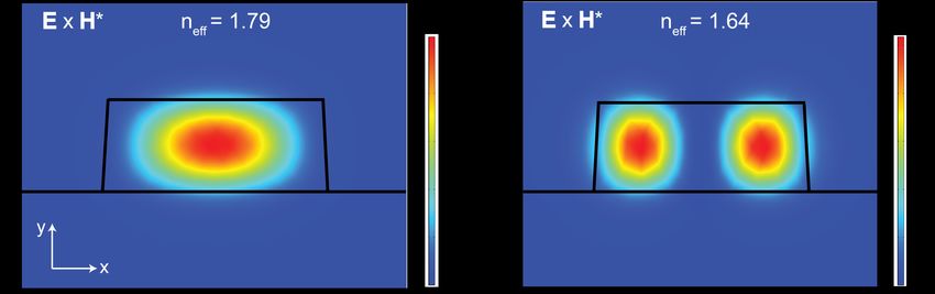
Figure 2.1: Simulation results of a Si3 N4 waveguide with height 660 nm and
width 1600 nm based on COMSOL. The sidewall angle of the waveguide is 87°.
The modes profiles of the Poynting vector in z direction for fundamental TE mode
(a) and second-order TE mode (b) are presented.
solve the modified Helmholtz equation. The FEM solver outputs the eigenvectors
(modes) and corresponding eigenvalues (propagation constant of the modes). The
propagation constant β accounts for the phase delay accumulated per unit length for
light of a certain wavelength propagating along the direction of invariance symmetry.
From the propagation constant, the effective index (neff ) of the mode can be defined
as
β
neff = , (2.1)
k0
where k0 is the wavenumber in vacuum, k0 = 2π/λ0 . λ0 is the wavelength in vac-
uum. An example of the simulated mode field of a waveguide (Si3 N4 core and SiO2
cladding) with height 660 nm and width 1600 nm at the wavelength of 1550 nm
is shown in Fig. 2.1. For TE polarization, the waveguide supports two transverse
modes, i.e., fundamental TE mode and second-order TE mode. The effective index
is 1.79 for fundamental TE mode, and is 1.64 for second-order TE mode.
The effective area, Aeff , is introduced in order to quantitatively evaluate the area
that the mode of a waveguide effectively covers in the transverse dimension, and has
expression as [72]
| ~E × H~ ∗ · ẑdA |2
R
Aeff = R , (2.2)
| ~E × H
~ ∗ · ẑ |2 dA
where ~E and H
~ are electric field and magnetic field, respectively. The integral should
be taken over the entire cross section. The effective area of a waveguide can be
dramatically modified by engineering the waveguide geometry. The mode profile
102.2. Dispersion engineering
of a Si3 N4 waveguide (660nm×1600nm) has an Aeff less than 1 µm2 whereas a
Si3 N4 waveguide with core cross-section dimension 150nm×1000nm results in an
Aeff larger than 5 µm2 , see Fig. 2.2a and b. The effective area of the fundamental TE
mode with respect to different waveguide geometries is shown in Fig. 2.2c.
A waveguide with small effective area indicates high optical intensity can be achieved
with reasonable optical power assuming the light source can efficiently excite the cor-
responding mode, which is essential for nonlinear optics. The smallest effective area
for a Si3 N4 waveguide is 0.75 µm2 and is achieved by a height of 500 nm and a width
of 1000 nm. However, it features normal dispersion (described in next section). In
order to achieve anomalous dispersion, the Si3 N4 waveguides need to be thick and
wide enough, as illustrated in Fig. 2.2c. Strip Si3 N4 waveguides designed to attain
anomalous dispersion in the telecommunication region are multimode.
Moreover, a waveguide with small effective area also dictates the possibility to achieve
small bending radius, which is beneficial for dense photonic integration. While
a small effective area is beneficial for nonlinear optics and compact integration, a
waveguide with large effective area is commonly used to match the optical mode
field between a waveguide and an optical fiber to reduce coupling losses [73]. More-
over, typically, weakly confined waveguides have much lower propagation losses
than high confinement waveguides, and find their applications in ultralow-loss delay
lines [35] and ultra-narrow linewidth lasers [74, 75].
2.2 Dispersion engineering
The propagation constant is in reality wavelength (frequency) dependent, and can be
expanded in Taylor series. The Taylor expansion of β around an angular frequency
ω0 is
∞
βn
β (ω) = β0 (ω0 ) + β1 (ω − ω0 ) + ∑ (ω − ω0 )n , (2.3)
n=2 n!
where β1 is related to the group velocity by vg = 1/β1 . βn is nth -order dispersion at
angular frequency ω0
dnβ
βn = , (2.4)
dω n
Here, β2 (group velocity dispersion parameter, and it’s later referred to dispersion.)
describes the pulse broadening along propagation. A waveguide has normal disper-
sion when β2 > 0, while has anomalous dispersion when β2 < 0. The dispersion
11Chapter 2. Optical waveguide characteristics
Figure 2.2: Mode profiles of fundamental TE mode of Si3 N4 waveguides with
geometries 660nm ×1600nm (a) and 150nm×1000nm (b). (c) Effective area of
fundamental TE mode of the waveguides with different geometries. The green
contour lines show the number of modes that the waveguide supports in TE po-
larization. The red contour lines show the dispersion of the fundamental TE mode
of the waveguides at the wavelength 1550 nm.
of the modes has two contributions, from the material and the waveguide geome-
try. The material dispersion of Si3 N4 and SiRN (used in [Paper A]) is shown in Fig.
2.3a. Due to the absorption resonance at the ultraviolet wavelength, the material dis-
persion is normal at short wavelengths (< 1650 nm). The dispersion originated from
the confinement of a waveguide can be simulated by setting the refractive indices of
core and cladding material constant at all frequencies. Here, the refractive indices of
Si3 N4 , SiRN (used in [Paper A]) and SiO2 are set to 1.99, 2.07 and 1.443, respec-
tively. The simulation results can be seen in Fig. 2.3b. The dispersion originated
from the confinement of a waveguide is anomalous at short wavelengths and normal
at long wavelengths, i.e., opposite to the material dispersion. The SiRN waveguide
features stronger anomalous dispersion than Si3 N4 , due to its higher index contrast to
the cladding layer. By properly selecting waveguide materials and geometries, a va-
riety of dispersion profiles can be acquired. It needs to be pointed out that the overall
dispersion of a waveguide can’t be simply calculated by adding material dispersion
to the dispersion originated from the confinement of a waveguide. The simulations
of the waveguide modes should be carried out considering the frequency dependent
refractive index of both core and cladding materials.
122.2. Dispersion engineering
Figure 2.3: a) Dispersion of bulk Si3 N4 and SiRN materials. b) Dispersion
originated from the confinement of Si3 N4 and SiRN waveguides. The waveguide
geometry is 800 nm × 1600 nm.
It’s worthwhile to see how sensitive the waveguide dispersion is to small varia-
tions of the waveguide geometry or the refractive indices of the materials. Fig. 2.4a
shows the dispersion of the fundamental TE mode of a Si3 N4 waveguide (660 nm
× 1600 nm) and two waveguides with slightly modified height (+ 10nm) and width
(+ 100nm). As can be seen, with 100 nm difference of waveguide width, the slope
of β2 is slightly changed, i.e., β3 is changed. With an increased height of 10 nm,
the waveguide dispersion is down shifted by ∼10 ps2 /km. In practice, although the
waveguide width can be precisely controlled by lithography with an accuracy < 10
nm, it’s difficult to avoid ∼ 2% variation of waveguide height across a wafer due to
LPCVD Si3 N4 deposition (see section 5.2). Additional to the variations of waveg-
uide geometries, the dispersion changes due to small variations of material refractive
index are shown in Fig. 2.4b. Here, the refractive index of Si3 N4 is offset by ±0.005
on purpose. It’s obvious that, by offsetting the refractive index by ±0.005, the waveg-
uide dispersion dispersion is up/down shifted by ∼ 7 ps2 /km. Note, only refractive
index offset is considered here, and more dispersion variation can be observed if the
wavelength dependent refractive index is taken into account. This indicates that the
refractive index of the materials should be precisely measured prior to the fabrication
of waveguides. The above analysis conveys that the variation of dispersion should be
carefully taken into account when precise dispersion engineering is needed, e.g., for
dispersive wave engineering [76] and octave-spanning DKS microcomb [45, 65, 77].
13Chapter 2. Optical waveguide characteristics
Figure 2.4: Sensitivity of group velocity dispersion parameter to waveguide pa-
rameters. (a) Si3 N4 waveguides with small variations of height or width. (b)
Waveguides with small variations of the refractive index of the core material.
14Chapter 3
Waveguide losses
The optical waveguide is the most fundamental element of any photonic integrated
component. Undesired waveguide losses can result in significant power attenuation
and crosstalk, thus undermining the possibility to create complex PICs. Waveguide
losses include scattering losses and absorptive losses. This chapter introduces the
origins of waveguide losses including design imperfections, bending losses, waveg-
uide imperfections and material losses. The characterization methods for waveguide
loss used in this Thesis are also introduced.
3.1 Origin of waveguide losses
3.1.1 Bending losses
In complex PICs, it’s unavoidable to introduce bent waveguides to modify the propa-
gation direction of the light. When a waveguide is dramatically bent, the phase front
of the optical mode at the outside of the bend needs to travel faster than the inner
side of the bend, and couples to radiation modes when it tends to travel faster than the
speed of light in the cladding layer [78]. Therefore, bending loss should be taken into
account for bent waveguides. Typically, the bending radius of a waveguide should
be maintained large enough so that the bending loss is negligible compared with
waveguide losses introduced from fabrication imperfections. This bending radius is
referred to as minimum bending radius. The minimum bending radius is related to
15Chapter 3. Waveguide losses
Figure 3.1: Simulated bending loss of a Si3 N4 waveguide with Aeff =0.85 µ m2
(blue circles), and a Si3 N4 waveguide with Aeff =2.39 µ m2 (orange circles).
the effective area of the waveguide mode. The simulated bending losses of a Si3 N4
waveguide (660 nm × 1600 nm) with Aeff =0.85 µm2 and a Si3 N4 wavguide (200 nm
× 1500 nm) with Aeff =2.39 µm2 at wavelength of 1550 nm are shown in Fig. 3.1.
Both results are based on the fundamental TE mode of the waveguides. A minimum
bending radius of 16 µm is sufficient for the high confinement Si3 N4 waveguide
in order to achieve bending loss less than 0.1 dB/m. Such small bending radii are
critical for DKS microcombs with repetition rates of ∼1 THz, which are described
in [Paper B, F]. However, a minimum bending radius of 100 µm is needed for the
low confinement Si3 N4 waveguide to achieve bending loss less than 0.1 dB/m. Due
to the increased minimum bending radii, low confinement waveguides significantly
increase the footprint of PICs.
3.1.2 Design imperfections
Design imperfections include (but not limited to) the improper design of both GDSII
files and curves used to connect different bends.
163.1. Origin of waveguide losses
Squaring the circles
GDSII files containing the patterns of waveguides are used to guide EBL for waveg-
uide fabrication. If a GDSII file with a coarse grid is used, the waveguide patterns
can be significantly distorted. The distorted patterns can be translated into the fabri-
cated waveguides through EBL and, consequently, introduce scattering losses. Apart
from the required fine grid for GDSII files, sufficient polygons should be used for
the patterns of bent waveguides so that the aliasing resulting from a finite number
of polygons is much smaller than the waveguide roughness introduced during nano-
fabrication [79]. A guideline for the required number of polygons for creating a
circle is
r
2πR 2
R − R2 − ( )
σ, (3.1)
2N
where R is the radius of a circle, σ is the RMS roughness of the fabricated waveg-
uides and N is the number of polygons for a circle. In this thesis work, 4000 polygons
are used for a circle with radius of 220 µm. This means the aliasing resulting from
squaring the circle is 0.06 nm, which is much smaller than the RMS roughness (1
nm) reported in [Paper B]. Although squaring the circles can be a severe imperfec-
tion in EBL, this problem is less significant in DUV stepper lithography due to the
demagnification factor.
Matching modes in bends
In PICs, bent waveguides are commonly used for 90°/180° turns and connections
between clockwise and counter-clockwise spiral waveguides. The mode mismatch
between waveguides with different curvatures can significantly introduce radiation
loss and coupling between different transverse modes. Therefore, Euler bend [80]
and modified versions [81, 82] were proposed to keep the curvature of the waveg-
uide continuous along propagation. Even though the solutions based on Euler bends
work well for connections between straight waveguides, it’s difficult to apply them
on two arbitrary bends as the solution is based on the symmetry of the structure. In
fact, a more general design algorithm was proposed earlier in [83] to minimize the
variation of the curvature [84], which in turn minimizes the coupling from the funda-
mental mode to other transverse modes [83]. The proposed solution to the problem
17Chapter 3. Waveguide losses
Figure 3.2: The physical position, the tangent, the curvature and the change of
the curvature with respect to the arc length s are presented in (a), (b), (c) and (d),
respectively. The bend is used to connect the clockwise and counter-clockwise
Archimedean spirals.
183.1. Origin of waveguide losses
of minimization of the variation of the curvature is [85]
κ(s) = a0 + a1 s + a2 s2 + a3 s3 , (3.2)
where κ (with unit µm−1 ) is the curvature with respect to arc length s from the start
point of the bend. Coefficients a0 , a1 , a2 , a3 need to be solved using the physical
position, the tangent of the bend, the curvature and the change of the curvature at the
start and end points as boundary conditions. The physical position, the tangent, the
curvature and the change of the curvature at the end of the curve are
Z s1
x1 = Re{ exp[iθ (s)]ds}, (3.3)
0
Z s1
y1 = Im{ exp[iθ (s)]ds}, (3.4)
0
Z s1
θ1 = θ0 + a0 + a1 s + a2 s2 + a3 s3 ds, (3.5)
0
κ1 = a0 + a1 s1 + a2 s21 + a3 s31 , (3.6)
dκ(s)
κ10 = , (3.7)
ds s=s1
where θ0 is the tangent of the bend at the start point. Here, Eqs. 3.3 and 3.4 do not
have analytical solutions. The equations can be solved numerically as described in
appendix-A. This bend design was used in [Paper D, E] to minimize the coupling
between different transverse modes. To exemplify this bend, the physical position,
tangent of the bend, the curvature and the change of the curvature of the bend are
shown in Fig. 3.2. The bend is used to connect the clockwise and counter-clockwise
Archimedean spirals (r=R+Aφ , where R=100 µm and A=10/π). The star symbols in
Fig. 3.2 indicate the corresponding values at the start point of the Archimedean spi-
ral, which should match that of the end point of the bend. Optical microscopy images
of a fabricated Archimedean spiral waveguide and a snail-shaped microresonator are
shown in Fig. 3.3.
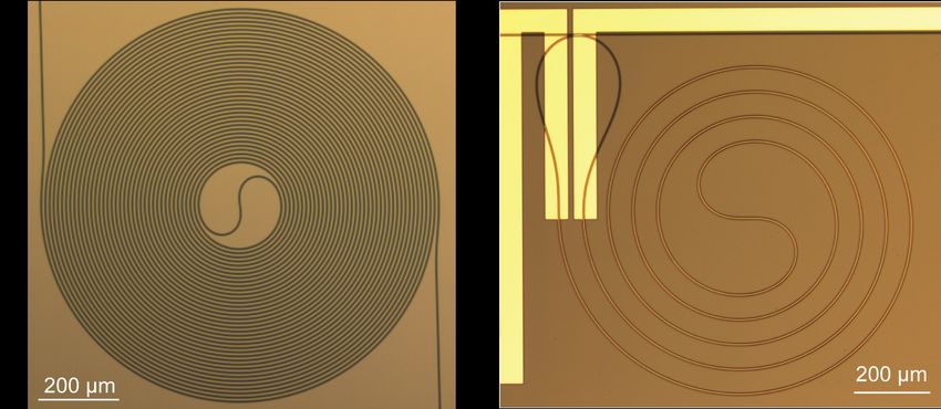
3.1.3 Mode coupling due to interfacial inhomogeneities
The interfacial inhomogeneities of a waveguide typically include surface roughness
and sidewall roughness. Surface roughness mainly comes from material deposition,
while sidewall roughness is mainly introduced during lithography and dry etching,
19Chapter 3. Waveguide losses
Figure 3.3: Optical microscopy images of an Archimedean spiral waveguide (a)
and a snail-shaped microresonator (b)
see more details in Chapter 5. The interfacial inhomogeneities of the waveguide
introduce a dielectric perturbation, which breaks the orthogonality relation between
the modes, thus allowing coupling from the intended guiding mode to other modes
including different transverse modes and radiation modes [78]. The coupling only
happens in the perturbation regime, and the coupling constant is determined by the
overlap of the coupled modes.
Although similar interfacial inhomogeneities can be achieved in waveguides with dif-
ferent geometries and refractive index contrast, their impact on the scattering losses
can be different. In order to qualitatively evaluate how sensitive the different waveg-
uide geometries are to the scattering loss induced from interfacial inhomogeneities,
we can simply evaluate the propagation loss by [36]
∂ neff ∂ neff
αr ≈ A[ + ], (3.8)
∂w ∂h
where w and h is the width and height of the waveguides, respectively. A is a scaling
factor which takes into account both the RMS roughness and correlation length of in-
terfacial inhomogeneities, while A is independent on the waveguide geometry. This
equation can be understood by the ’sensitivity’ of the effective index of the mode to
the variations of width and height produced by the sidewall roughness and surface
roughness, respectively. Since the sidewall roughness and surface roughness of the
waveguide typically differs significantly from each other, we calculate ∂ neff /∂ w and
203.1. Origin of waveguide losses
Figure 3.4: The fundamental TE mode of (a) ∂ neff /∂ w and (b) ∂ neff /∂ h with
respect to different waveguide geometry.
∂ neff /∂ h separately. Fig. 3.4a and b illustrates the variation of the effective index of
the mode with the waveguide geometry for Si3 N4 waveguides at the wavelength 1550
nm. Since ∂ neff /∂ w represents the ’sensitivity’ to sidewall roughness, Fig. 3.4a in-
dicates that thin and wide waveguides are less sensitive to the scattering loss induced
from sidewall roughness. However, this type of waveguides are unsuitable for non-
linear optics based on the analysis in Chapter 2. In fact, we need sufficient thick
waveguides in order to achieve anomalous dispersion, and to be relatively narrow to
maintain small effective area. Hence the waveguide with this type of design is very
susceptible to the sidewall roughness. It’s clear that advanced nanofabrication tech-
niques are required to attain Si3 N4 waveguides with sidewalls as smooth as possible.
Fig. 3.4b indicates that thicker waveguides are less sensitive to surface roughness,
and this is in line with the requirement of Si3 N4 waveguide designs for nonlinear
optics.
In order to accurately and quantitatively model the waveguide radiation loss due
to sidewall roughness, three-dimensional models of waveguide scattering loss are
needed [86, 87]. In [86], the model is based on the volume current method, where
variations of dielectric constant on waveguide sidewalls are considered as equivalent
current densities. In [87], radiated light due to waveguide roughness is considered
to be coupled to radiation modes. Both [86] and [87] constructed three-dimensional
radiation modes taking the high refractive index of the core material into account.
However, unfortunately, these two references draw conclusions that are opposite to
each other. Ref [87] concludes that 2D model [88] underestimate the waveguide loss
21Chapter 3. Waveguide losses
compared with 3D model, while [86] concludes the opposite.
Notwithstanding, according to the models from both [86–88], waveguide scattering
loss is linearly proportional to squared RMS roughness σ 2 , indicating that ultra-
smooth surfaces are required to reach ultralow-loss scattering losses in high con-
finement waveguides. At the start point of this thesis work, the RMS roughness of
waveguide sidewalls was ∼ 5 nm [56]. But, at the late stage of this PhD, this value
has been reduce to less than 1 nm [Paper B]. This corresponds to more than 25 times
reduction of scattering loss due to sidewall roughness. The SEM images showing
the evolution of the fabricated Si3 N4 waveguides are shown in Chapter 5, Fig. 5.5.
The RMS roughness of the top and bottom surfaces of the waveguides is ∼ 0.5 nm
for SiRN [56][Paper A], while it’s less than 0.2 nm for Si3 N4 waveguides. This cor-
responds to more than 4 times reduction in scattering loss originating from surface
roughness.
It has to be remarked again that all the Si3 N4 waveguides used in this thesis are multi-
mode waveguides due to required anomalous dispersion. The fundamental mode of
a waveguide can be coupled to higher-order modes due to sidewall roughness. This
can be modeled by modified coupled-power theory based on [87, 89]. Here, coupled-
power theory is only valid for weak coupling between different transverse modes,
i.e., a complete exchange of power between two modes requires a distance much
larger than the wavelength. Since we are considering the weak coupling due to weak
sidewall roughness, this approximated theory is valid. Considering all the power is
carried at the fundamental mode (µ) at the initial point of a waveguide, the coupled
power equation due to one waveguide sidewall can be written as [89]
dPµ N
= −(2αµ + ∑ hµν )Pµ , (3.9)
dz ν=1
where Pµ is the power carried by the fundamental mode µ, 2αµ is the propagation
loss of mode µ, and ν indicates all the other guided modes that carry power apart
from µ mode. hµν are the coupling coefficients between modes µ and ν, and are
described as
hµν =| K̂µν |2 h| F(βµ − βν ) |2 i, (3.10)
Here, the spectral density of waveguide roughness h| F(βµ − βν ) |2 i is
2σ 2 1
h| F(βµ − βν ) |2 i = , (3.11)
Lc (βµ − βν )2 + 1/Lc2
223.1. Origin of waveguide losses
(i) (e) (i) (e)
where Lc is the correlation length. | K̂µν |2 =| K̂µν |2 + | K̂µν |2 . K̂µν and K̂µν account
for the coupling between mode µ and ν, due to the field at the internal and external
sides of waveguide edge, respectively. They are described as [87]
Z d
(i) iωε0 2 ∗ ~
K̂µν = (n − n21 ) dy[~Eµt · Eνt ]x=w−σ /2 , (3.12)
4P 2 −d
Z d
(e) iωε0 2 ∗ ~
K̂µν = (n − n21 ) dy[~Eµt · Eνt ]x=w+σ /2 , (3.13)
4P 2 −d
where P is the total power of the guided mode, ε0 is permittivity in vacuum, n2 and n1
are the refractive index of the core and clad materials, respectively. ~Eµt and ~Eνt are
transverse parts of electrical field of mode µ and ν, respectively. Waveguide width
is 2w, and height is 2d. A Si3 N4 waveguide with height 700 nm and width 2000
nm is used as an example for coupling loss calculation at wavelength of 1550 nm.
The waveguide supports 3 transverse modes in TE polarization (TE0 , TE1 and TE2 )
and 3 transverse modes in TM polarization (TM0 , TM1 and TM2 ). The mode field
of different transverse modes at wavelength 1550 nm are simulated using Lumeri-
cal Mode, and the coupling coefficients 2hµν (considering coupling due to sidewall
roughness from both sidewalls of the waveguide) for both TE and TM polarization
with respect to different correlation lengths are calculated and shown in Fig. 3.5. The
coupling is undesirably maximized when correlation length is 1/ | βµ − βν |. Since
attaining correlation length larger than 1.5 µm seems to be difficult [52, 90][Paper
B], it’s beneficial to have small correlation length. The coupling from TE0 to TE2 is
overall much stronger than that to TE1 since the electric field of TE2 at the waveg-
uide edge is much larger than that of TE1 . With σ =1nm and Lc =500 nm reported in
[Paper B], the loss due to coupling from TE0 to TE1 is 0.34 dB/m, and is 0.77 dB/m
from TE0 to TE2 . The total propagation loss of the waveguides was measured to be
∼ 3 dB/m.
In addition to the coupling between different transverse modes, which only hap-
pens in multi-mode waveguides, sidewall roughness of a waveguide can introduce
coupling from the forward-propagating mode to the backward-propagating mode.
In fact, since back-scattering coefficient scales with (∂ neff /∂ w)2 [91], this effect is
more significant for high confinement single-mode waveguides, seeing Fig. 2.2 and
3.4. The power of back scattered light increases exponentially due to periodic side-
wall roughness, which can be regarded as Bragg scattering, whereas the power of the
back scattered light increases linearly due to random sidewall roughness [89]. This
provides a guideline for the nano-fabrication of waveguides. In this thesis work, we
23Chapter 3. Waveguide losses
Figure 3.5: Coupling from the fundamental mode to higher-order modes due to
sidewall roughness from both sidewalls. The Si3 N4 waveguide geometry is height
700 nm and width 2000 nm. a) TE polarization. b) TM polarization. The coupling
loss is normalized to squared RMS roughness in squared nanometers.
observed a relatively weak resonance splitting in microresonators due to the coupling
between clockwise- and counter-clockwise propagating modes. This effect will be
described in section 3.2.2.
3.1.4 Material losses
Material losses can include absorptive and scattering losses. The absorptive losses
include intrinsic absorption due to electronic transitions and vibrational transitions
[78], as well as extrinsic absorption due to contaminants introduced during material
deposition and any post-processes. Electronic transitions refer to electrons getting
energy from photons and raising from the valence band to the conduction band. This
effect is almost negligible in both Si3 N4 and SiO2 at the telecommunication band,
due to their large bandgap > 4 eV. Absorption due to vibrational transitions results
from molecule vibrational modes, e.g., bending and stretching modes. In contrast
to electronic transitions in ultraviolet wavelength, vibrational transitions typically
result in absorption in the infrared region. Si3 N4 films deposited from precursors
SiH2 Cl2 and NH3 have undesired N-H bonds, which result in vibrational transition
in wavelength near 1510 nm [92]. Even though high temperature (>1100 °C) is im-
plemented to outgas hydrogen [93–95], the residual of N-H bonds can still result
in non-negligible absorption near 1510 nm in ultra-high Q Si3 N4 microresonators
24You can also read