Optimization and Design of Passive Link with Single Channel 25 Gbps Based on High-Speed Backplane
←
→
Page content transcription
If your browser does not render page correctly, please read the page content below
electronics
Article
Optimization and Design of Passive Link with Single Channel
25 Gbps Based on High-Speed Backplane
Jie Liu * , Kai Zhang *, Qiang Wu, Li Peng, Kai Yao and Hu Liu

                                          Faculty of Information Technology, Beijing University of Technology, Beijing 100124, China;
                                          qiangwu@bjut.edu.cn (Q.W.); PengLi@emails.bjut.edu.cn (L.P.); yaokai@emails.bjut.edu.cn (K.Y.);
                                          liuhu16@emails.bjut.edu.cn (H.L.)
                                          * Correspondence: liujie217@bjut.edu.cn (J.L.); KaiZhang@emails.bjut.edu.cn (K.Z.); Tel.: +86-158-0137-8572 (J.L.);
                                            +86-150-1018-9818 (K.Z.)

                                          Abstract: In recent years, with the development of the communication industry, the need to use
                                          Ethernet switches to transmit big data has become more urgent, and its protocol standards are
                                          iterating towards higher return loss, wider bandwidth, lower impedance fluctuations and insertion
                                          loss. Based on the research of high-speed backplane with a single channel 25 Gbps transmission rate,
                                          a novel double grounded planar strip coplanar waveguide design is presented, which significantly
                                          improved return loss to 20 dB and reduced insertion loss, which meet the loss standard of 100GBASE-
                                          KR4. The resonant cavity model of transmission line reference plane is improved by introducing
                                          vias and the parameters of vias in the reference plane are studied to reduce the impact of resonance,
                                          which improved the transmission −1 dB bandwidth to 60 GHz. Based on equivalent circuit analysis
                                          of differential vias’ joint reverse pad, the parameters related to the differential vias are studied, the

                                   impedance fluctuation is reduced to 100 ± 3 Ω, which is 70% better than the impedance fluctuation
Citation: Liu, J.; Zhang, K.; Wu, Q.;     standard (100 ± 10 Ω) of 100GBASE-KR4. After optimizing the mathematical model of strip coplanar
Peng, L.; Yao, K.; Liu, H.                waveguide, reference plane and differential vias, we built a simulation model of the backplane
Optimization and Design of Passive        passive link which met the 100GBASE-KR4 backplane Ethernet specification. In the actual test, it was
Link with Single Channel 25 Gbps          found that the optimized model can improve the link performance.
Based on High-Speed Backplane.
Electronics 2021, 10, 1773. https://      Keywords: high-speed passive link; 25 Gbps; strip coplanar waveguide; via; 100GBASE-KR4
doi.org/10.3390/electronics10151773

Academic Editors: Chua-Chin Wang
and Arezki Benfdila                       1. Introduction
                                                With the rapid development of the global Internet, with cloud computing, mega
Received: 22 June 2021
Accepted: 22 July 2021
                                          data and 5G communication services gradually entering people’s lives, there are greater
Published: 24 July 2021
                                          requirements for data exchange rate and bandwidth. The concept of backplane Ethernet
                                          first appeared in the IEEE 802.3ap standard issued by IEEE in 2007. At that time, IEEE not
Publisher’s Note: MDPI stays neutral
                                          only proposed the concept of backplane Ethernet, but also released 10GBASE-KR back-
with regard to jurisdictional claims in
                                          plane Ethernet specification [1] for the proposed concept of backplane Ethernet. In recent
published maps and institutional affil-   years, the development of Ethernet is even more amazing, IEEE has successively released
iations.                                  100G application specifications [2]. The 100GBASE-KR backplane Ethernet specification has
                                          begun to challenge the single channel rate of 25 Gbps. With the development and maturity
                                          of Ethernet specification, it can not only be used in switches, routers and other network
                                          communication equipment, but also be applied to embedded switching equipment such as
Copyright: © 2021 by the authors.
                                          automation of power distribution networks and intelligent traffic road monitoring systems.
Licensee MDPI, Basel, Switzerland.
                                                Due to the development and improvement of single channel rate from 10 Gbps to
This article is an open access article
                                          25 Gbps [3–6], the requirements for high-speed system circuit design are also increased. The
distributed under the terms and           current research and development of high-speed systems mainly focuses on two aspects:
conditions of the Creative Commons        (1) increasing the transmission rate without sacrificing the reliability and stability of the
Attribution (CC BY) license (https://     system; (2) the control of production cost [7,8]. To achieve single channel 25 Gbps rate
creativecommons.org/licenses/by/          transmission on the circuit, the operating frequency of the system will inevitably exceed
4.0/).                                    12 GHz, which means that the traditional circuit interconnection design has difficultly

Electronics 2021, 10, 1773. https://doi.org/10.3390/electronics10151773                                      https://www.mdpi.com/journal/electronics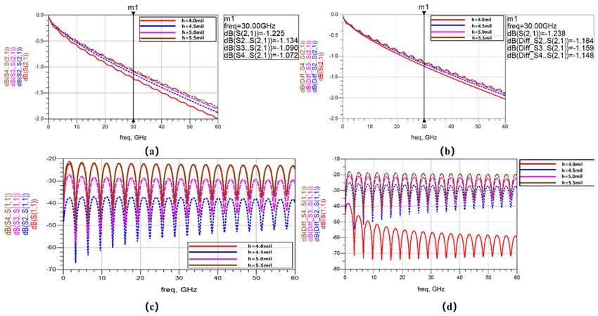
Electronics 2021, 10, 1773                                                                                          2 of 17

                             guaranteeing the transmission performance of a high-speed system. Signal integrity
                             problems, such as reflection and crosstalk, in high-speed circuit design have serious impacts
                             on circuit performance [9].
                                  In order to ensure the high-speed transmission of the backplane passive link with
                             25 Gbps transmission rate, and reduce the design time and cost, it is necessary to carry
                             out modeling and finite element simulation of the relevant components of the passive
                             link at the beginning of the backplane design [10–12]. Compared with the full-wave 3D
                             simulation experiment of single transmission line with 25 Gbps transmission rate carried
                             out by Peerouz Amleshi [13], the return loss of single transmission line is 10 dB and
                             the impedance fluctuation is 100 ± 15 Ω. In this paper, the strip coplanar waveguide
                             transmission line model is innovatively proposed, which can increase the return loss to
                             20 dB. Based on the equivalent circuit model of the differential vias that is innovatively
                             established, the impedance fluctuation can be reduced to 100 ± 3 Ω. The validity of signal
                             transmission is guaranteed.
                                  As the electromagnetic waves will produce resonance when entering the conductor
                             cavity, insertion loss fluctuated sharply at the resonance point, leading to the reduction of
                             output efficiency. In the simulation of the 40 Gbps signal transmission studied by Chang
                             Fei Yee, the −1 dB bandwidth of the signal transmission is 40 GHz, and there is a resonance
                             point in the adjacent frequency band after 40 GHz [14]. The mathematical modeling and
                             simulation study on the strip coplanar waveguide transmission line reference plane is
                             carried out in this paper, so that the insertion loss had no resonance within the 60 GHz
                             bandwidth, and the reliability of signal transmission is guaranteed.
                                  In this paper, we study the modeling of transmission line, reference plane and vias, and
                             conduct the optimization design including: (1) in order to correct the loss, modeling and
                             analysis of transmission line based on strip coplanar waveguide; (2) modeling and analysis
                             based on strip coplanar waveguide transmission line reference plane which increased
                             passband width; (3) modeling and analysis of differential vias which reduced impedance
                             fluctuations; (4) the passive link model of high speed backplane is established.

                             2. Materials and Methods
                             2.1. System Composition
                                  In this paper, the signal integrity of the passive link on the backplane in the whole
                             serial link across the backplane system is studied. The passive link on the backplane mainly
                             includes high-speed connector, via and transmission line. The strip coplanar waveguide of
                             transmission line, strip coplanar waveguide transmission line reference plane and vias are
                             shown in the Figure 1.

                             Figure 1. Schematic diagram of high-speed passive link.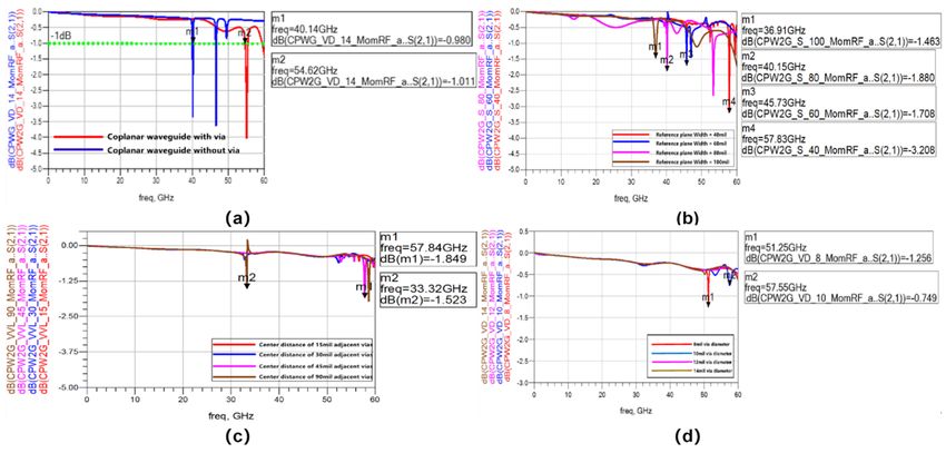
Electronics 2021, 10, 1773 3 of 17
Three aspects are simulated and optimized: (1) the best height of strip coplanar
waveguide metal plate is determined by simulation, the insertion loss was reduced and
the return loss was increased to 20 dB, which meet the 100GBASE-KR backplane Ethernet
specification; (2) the factor of the transmission line reference plane affecting the resonant
frequency are deduced, and the optimal parameters are determined by simulation, so
that the signal transmission bandwidth of −1 dB can reach 60 GHz; (3) an equivalent
circuit model is established for the differential vias, and the simulation results show that
impedance fluctuation with the best via parameters is 100 ± 3 Ω. Simulation guides
the design of the actual circuit. After integrating the above three aspects of simulation
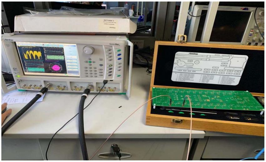
optimization design, the actual test is shown in Figure 2.
Figure 2. Environment of actual test.
2.2. Strip Coplanar Waveguide Transmission Line
Modeling and Analysis of Strip Coplanar Waveguide
Coplanar waveguide transmission lines are mainly used in the current backplane de-
sign. There are two kinds of common coplanar waveguide structures, one is the traditional
coplanar waveguide (CPW) structure [15,16], the other is the coplanar waveguide with
ground (CPWG) structure, shown in Figure 3a,b, respectively.
Figure 3. Various waveguide structures. (a) Section of traditional coplanar wave; (b) cross section of
coplanar waveguide with metal substrate; (c) cross-sectional view of ribbon coplanar waveguide.
The electromagnetic field of coplanar waveguide is mainly distributed near the in-
terface between the medium below the transmission line and the air above. Due to the
existence of alternating electric field between the central metal conduction band and the
adjacent grounding conductor, the coplanar waveguide transmits TEM wave with no
cut-off frequency. The introduction of adjacent ground conductor planes on both sides of
coplanar waveguide makes it difficult to interfere, which improves the electromagnetic
compatibility of transmission line [17].
Coplanar waveguide supports quasi TEM propagation mode. Coplanar waveguide
transmission line is more convenient for the interconnection of active or passive devices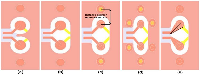
Electronics 2021, 10, 1773                                                                                                        4 of 17

                                  on the surface, and its radiation and crosstalk are also smaller. In addition, the copla-
                                  nar waveguide transmission line also has extremely wide bandwidth and small disper-
                                  sion, but the traditional coplanar waveguide has obvious disadvantages that the loss is
                                  relatively large.
                                        With dense wiring, it is impossible to lay all high-speed wiring in the form of CPW
                                  or CPWG on the top and bottom layers of printed circuit board, especially in the design
                                  of high-speed backplane, the number of high-speed transmission lines will increase a lot,
                                  and the inner layer high-speed wiring is inevitable. In this paper, based on the traditional
                                  coplanar waveguide model, a kind of inner striped coplanar waveguide transmission line
                                  structure is modeled and analyzed to explore the loss and transmission bandwidth of
                                  inner striped coplanar waveguide transmission line. The cross section of the strip coplanar
                                  waveguide is shown in Figure 3c. The additional upper and lower metal plates make the
                                  transmission line have better anti-interference and anti-radiation ability, so as to improve
                                  return loss and reduce insertion loss of the transmission line.
                                        The single ended strip coplanar waveguide is modeled and analyzed, and its parame-
                                  ters are shown in Figure 4c. The modeling of differential coplanar waveguide is similar to
                                  that of single ended waveguide as shown in Figure 4d.

      Figure 4. (a) Diagram of traditional coplanar waveguide structure; (b) schematic diagram of traditional differential coplanar
      waveguide structure; (c) single-ended strip coplanar waveguide structure diagram with upper and lower metal plates;
      (d) differential strip coplanar waveguide structure diagram with upper and lower metal plates.

                                        Characteristic impedance Z0 of strip coplanar waveguide, equivalent permittivity ε e f f
                                  of strip coplanar waveguide, phase velocity νph can be expressed as [18,19]:

                                                                                        1
                                                                              Z0 =                                                    (1)
                                                                                     C · v ph

                                                                                          c
                                                                             v ph = √            .                                    (2)
                                                                                          εe f f
                                                                                          C
                                                                               εe f f =                                               (3)
                                                                                          C0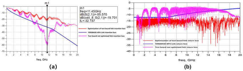
Electronics 2021, 10, 1773 5 of 17
c is the speed of light in vacuum. Unit length capacitance C of strip coplanar waveguide,
C0 is the line capacitance without any medium:
C = C0 + C1 + C2 + C3 + C4 (4)
where C1 and C3 are upper conductor capacitance, C2 and C4 are the capacitance of the
lower conductor, which can be expressed as:
K (k0 )
4ε 0 K (k i) i=0
i
K (k0 )
Ci = 2ε 0 (ε r1 − 1) K (k i) i = 1, 3 (5)
i
K (k0 )
2ε 0 (ε r2 − 1) K (k i) i = 2, 4
i
q
c b2 − a2
b c2 − a2
i=0
r
2 2
sinh(∏ c/2hi ) sinh (∏ b/2hi )−sinh (∏ a/2hi )
ki = i = 1, 2 (6)
sinh(∏ b/2hi ) sinh2 (∏ c/2hi )−sinh2 (∏ a/2hi )
tanh(πa/2hi )
i = 3, 4
tanh(πb/2hi )
p
k0 = 1 − k2 (7)
where K (k) represents the complete elliptic integral of the first kind. The parameters k
depend on the geometry of the transmission line.
From Equations (5) and (6), it can be concluded that the parasitic capacitance of the
strip coplanar waveguide is determined by the height of the metal plate, which further
affects the impedance of the strip coplanar waveguide, the insertion loss [20] and return
loss [21] will be directly affected.
2.3. Research on Transmission Line Reference Plane for 25 Gbps Rate Backplane
Coplanar Waveguide Reference Plane Modeling
If the electromagnetic wave enters a closed cavity made of conductor, it will be
continuously reflected in the cavity, the electric field and magnetic field will be converted to
each other, and alternately appear at the corresponding maximum field strength position,
thus forming a resonance state. There are two shock modes: TEmnp and TMmnp . The
resonance frequency of TEmnp and TMmnp is:
r
1 mπ 2 nπ 2 pπ 2
f mnp = √ + + (8)
2π µε a b l
where a, b and l are the geometrical parameters of the waveguide. m, n and p corre-
spond to the change number or half wave number of the field along a, b and l directions,
respectively [22].
In the finite grounded coplanar waveguide with a metal bottom plate, the adjacent
finite metal plane of the same layer of the transmission line and the metal plane of the
bottom plate are regarded as a resonant cavity with an open circuit at the edge. At the
resonant frequency of the resonant cavity, most of the electromagnetic energy is coupled
to the adjacent metal plane, and only a small part of the energy continues to propagate
along the transmission line. Therefore, due to the increase of reflection and radiation, the
transmission of useful signals is reduced.
The resonant frequency can be calculated from the size of a side grounded metal plane.
As shown in Figure 5a, it shows a resonant cavity composed of a side metal plane adjacent
to the transmission line and a metal bottom plate. Open boundary conditions are used in
all three plates. The parameters of the simulation of the coplanar waveguide transmission
line are shown in Figure 5b,c.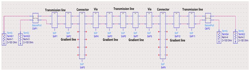
Electronics 2021, 10, 1773                                                                                                    6 of 17

      Figure 5. (a) Structure of multilayer coplanar waveguide with upper and lower metal plates; (b) sectional view of single-
      ended coplanar waveguide transmission line; (c) top view of single-ended coplanar waveguide transmission line.

                                      As the dielectric substrate in the circuit board is nonmagnetic, its relative permeability
                                 µr equals to 1, so permeability µ in the cavity model is equal to permeability µ0 in vacuum.
                                 In this model, the relative permittivity ε r is known. Therefore, the dielectric constant can
                                 be characterized by the relative dielectric constant.
                                                                                      q
                                                                                 c=           1
                                                                                          ε 0 · µ0
                                                                                                         εr
                                                                   ε = ε r · ε 0 −−−−−−→                 2
                                                                                                                                   (9)
                                                                                                     ( c ) · µ0

                                       In high-speed circuits, the dielectric height h is far less than the wavelength λ, Gener-
                                 ally, the influence of edge field is ignored. The formula is simplified as follows:
                                                                                      r
                                                                               c               m 2  n 2
                                                                ( f r )mn0   = √                   +                              (10)
                                                                              2 εr             L     W

                                 where L represents the length of the reference plane on the adjacent side of the transmission
                                 line, W represents the width of the reference plane on the adjacent side of the transmission
                                 line. When the reference plane of the adjacent side of the transmission line is connected
                                 to the metal base plate through the ground via, the boundary conditions of the resonator
                                 analyzed above will change. The via used for connection is regarded as a metal short-circuit
                                 plate, and the cavity satisfies the short-circuit boundary condition. In this case, the mode
                                 parameter m can be an integer or a natural number, while the parameter n can only be
                                 an integer multiple of 0.5. By modifying the model parameters, the Formula (10) is still
                                 valid under the condition of short circuit boundary.
                                       Due to the influence of via, the equivalent width should be corrected:
                                                                                               2
                                                                                         VD
                                                                    W·L−k·π               2
                                                            eW =                                     , k = 1, 2, 3 · · ·          (11)
                                                                                L
                                      The resonance frequency formula is revised to:
                                                                                     r
                                                                               c              m 2  n 2
                                                               ( f r )mn0    = √                  +                               (12)
                                                                              2 εr            L     eW

                                      It can be concluded from Equations (11) and (12), the width of the reference plane
                                 W, the number of vias on the reference plane k and the diameter of vias VD will affect the
                                 resonant frequency of the transmission line. The change of the number of vias k is actually
                                 changing the center distance VVL between the connected vias [23,24].

                                 2.4. Research on Via for 25 Gbps Rate Backplane
                                     In multilayer printed circuit board design, vias provide electrical connection paths
                                 between different layers. When the signal frequency is lower than 3 GHz, the parasitic effect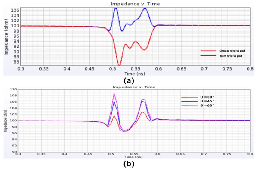
Electronics 2021, 10, 1773                                                                                                                                   7 of 17

                                    caused by the via structure has little influence on the transmission performance of the circuit
                                    and is generally ignored. However, with the increase of operating frequency, the existence
                                    of vias will make the impedance of the link discontinuous. At the same time, the parasitic
                                    capacitance and inductance introduced by via parasitic effect will also lead to reflection
                                    and scattering in the process of signal transmission, which will affect the performance of
                                    the link. Therefore, the research on the characteristics of vertical interconnected vias is not
                                    only of great significance to the simulation and design of multilayer circuit board, but also
                                    can better guide the analysis of signal integrity in high-speed digital circuits [25–28].

                                    Modeling and Analysis
                                    • Modeling and analysis of differential vias
                                         The specific parameters of differential vias are shown in Figure 6a. The equivalent
                                    circuit of differential vias is shown in Figure 6b, the two sides are π-type equivalent circuit
                                    with single via, and the middle part is mutual inductance part between two vias. In high
                                    frequency circuits, the actual shape of the reverse pads with differential vias is the form of
                                    circular and rectangular joint reverse pads. Then the differential vias of the joint reverse
                                    pad were analyzed.

                Figure 6. (a) Schematic diagram of differential vias section; (b) differential vias π-type equivalent circuit.

                                         The parasitic capacitance Cvia of the joint reverse pad differential vias is expressed by
                                    Equation (13), and the equivalent coaxial capacitance Ca and equivalent inductive capacitance
                                    Cb of the joint reverse pad differential vias are shown in Equations (14) and (15).
                                                                        s
                                                                             πR2b + 2Rb · Rs
                                                                Rdb =                                        Cvia = Ca + Cb                                   (13)
                                                                                  2π

                                                                                               2πε r ε 0 t
                                                                                    Ca =                                                                    (14)
                                                                                               ln RRdba

                                                                                                                         ( n ) ( n ) −1

                                                                                  8πε r ε 0 t
                                                                                                     2N −1           1−Γ Ra Γ R
                                                                       Cb =    h·ln( Rdb /R a )        ∑       2         (2)              ×
                                                 nh                                            i   n=1,3,5... k n · H0 (k n · R a )                      o    (15)
                                                       (2)                   (2)                       (n)
                                                      H0 (k n   · Rdb ) −   H0 (k n   · Ra )       + Γ R [ J0 (k n · Rdb ) − J0 (k n          · R a )]

                                    where t is the copper foil thickness of the reference layer, Ra is the pad radius of the joint
                                    reverse pad differential vias, Rdb represents the reverse pad radius of the joint reverse pad
                                                                                                           (2)
                                    differential vias, kn is the radial wave number, H0 () is the second Hankel function of
                                                   (n)
                                    order zero, Γ R represents the boundary condition.
                                         The pad diameter and reverse pad diameter of the via will affect the parasitic capaci-
                                    tance of the differential vias, and then affect the performance of the vias.
                                    • Modeling and analysis of via stump
                                         At present, the high-speed connector package on multilayer printed circuit board
                                    basically adopts to via design, from the top to the bottom. When the signal is transmitted
                                    from the sub-board to the backplane through the high-speed connector, it will be led out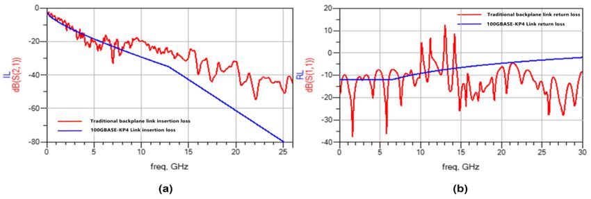
Electronics 2021, 10, 1773                                                                                            8 of 17

                             from different signal layers in the circuit board, so that the via will leave different lengths
                             of stumps.
                                  Based on the principle of quarter wavelength, the relationship between the length of
                             via stump and resonance frequency can be deduced. The relationship between the length
                             of through via and wavelength is expressed by the following equation:

                                                                           1     1 vp
                                                                 Lstub =     ·λ = ·                                    (16)
                                                                           4     4 fv

                             where Lstub is the length of through via residual pile, λ is the wavelength, v p is the trans-
                             mission rate of the signal, fv is the resonant frequency of the via.
                                  The transmission rate of the signal is v p which can be expressed by Equation (17), and
                             c represents the transmission speed of light in vacuum, ε r is the relative permittivity of the
                             medium around the via:
                                                                                c
                                                                        vp = √                                          (17)
                                                                                 εr
                                  The resonance frequency fv caused by through via residual pile is:
                                                                             c
                                                                   fv = √                                              (18)
                                                                       4 ε r · Lstub

                                  The depth of the residual pile through the via affects the impedance fluctuation. In
                             the current process design, the most commonly used technology is back drilling to remove
                             the redundant residual pile in the vias. However, the residual pile cannot be reduced too
                             much, which leads to the failure to meet the minimum reserved depth of the connector. We
                             study the influence of the depth of vias’ residual pile on impedance.
                             • Return via and tear drop.
                                  When the via is used as the signal transmission path in multilayer printed circuit
                             board, the return current of the signal will excite the parallel board mode between the
                             power layer and the formation, resulting in the electromagnetic coupling phenomenon.
                             The return via can provide an effective return path for the return current of the signal and
                             suppress the electromagnetic coupling effect. We studied the influence of number of return
                             vias and the distance between return via and signal via on impedance.
                                  For the signal integrity of the link, adding tear drop can smooth the impedance of the
                             connection between wire and pad, wire and via, so as to reduce the mutation of impedance
                             and avoid signal reflection caused by impedance mutation during high frequency signal
                             transmission. We studied the influence of tear drop angle on impedance.
                                  The main parameters to be determined in the above discussion are given in the
                             simulation modeling diagram, as shown in Figure 7.

                             2.5. Composition of Backplane Passive Link
                                  The evaluation of passive link performance is based on 100GBASE-KR4 standard of
                             Ethernet backplane published in IEEE 802.3bj. As shown in Figure 8, taking the single
                             channel link in 100GBASE-KR4 standard as an example, the passive interconnection channel
                             of the whole high-speed backplane is defined as the part between TP0 and TP5 and the
                             impedance is controlled at 100 ± 10 Ω. 100GBASE-KR4 standard also defines that the single
                             channel transmission rate of backplane is at least 25.78125 GBd ± 100 ppm, so that the total
                             rate of four channels can achieve the performance of 100G Ethernet transmission line.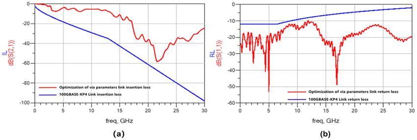
Electronics 2021, 10, 1773                                                                                                        9 of 17

      Figure 7. (a) Simulation modeling diagram of circular reverse pad; (b) simulation modeling diagram of joint reverse pad; (c)
      simulation modeling diagram of two return vias; (d) simulation modeling diagram of eight return vias; (e) via tear drop
      simulation modeling diagram.

                                 Figure 8. Schematic diagram of 100GBASE-KR4 single channel link.

                                       The 100GBASE-KR4 standard also defines the insertion loss (19) and return loss (20) of
                                  the whole high-speed backplane link, and the whole link must meet the loss value required
                                  in the standard. The insertion loss of backplane link is defined in 100GBASE-KR4 standard
                                  as follows:
                                                                      p
                                                              1.5 + 4.6 f + 1.318 f , 0.05 ≤ f ≤ f b /2
                                                IL( f ) ≤                                                   (dB)        (19)
                                                              −12.71 + 3.7 f , f b /2 < f ≤ f b

                                                                    12                           , 0.05 ≤ f ≤ f b /4
                                                  RLd ( f ) ≤                                                              (dB)      (20)
                                                                    12 − 15 log10 (4 f / f b )   , f b /4 < f ≤ f b
                                  where f is the signal frequency.
                                        A complete backplane passive link is built in ADS for simulation, and a channel
                                  in the backplane passive link is taken as an example for simulation verification. The
                                  model consists of two high-speed connectors, two pairs of differential vias and a coplanar
                                  waveguide transmission line. The connector and transmission line are interconnected
                                  by klopfenstein tapered transmission line [14,29–31]. The parameters of the high-speed
                                  connector are S-parameters provided by the official website of TE Connectivity [32]. The
                                  differential vias model adopts the traditional circular reverse pad via model and does not
                                  back drill the via stumps. The transmission line adopts the traditional microstrip coplanar
                                  waveguide transmission line. The S-parameter models of connector, via and transmission
                                  line are imported into ADS software for co-simulation. The S-parameter modeling diagram
                                  of the constructed complete transmission link is shown in Figure 9, in which the circuit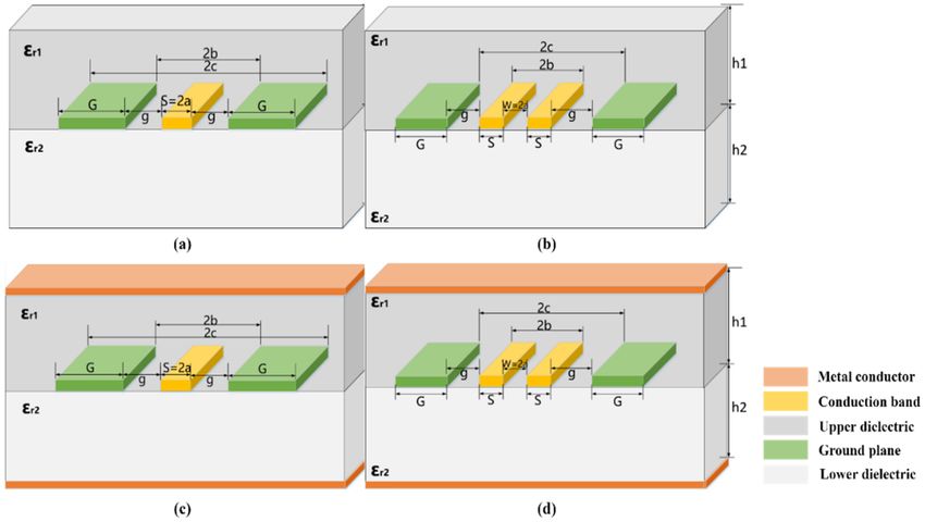
Electronics 2021, 10, 1773                                                                                                           10 of 17

                                   stack adopts the 10 layers board stack used in the previous simulation, and the transmission
                                   line length is set to 5000 mil [33–35].

                                 Figure 9. Modeling diagram of backplane full link S-parameter model.

                                   3. Results
                                   3.1. Simulation Results after Optimization of Each Part
                                   • Optimal strip coplanar waveguide metal plate height
                                        The finite element simulation software ADS was used to build the simulation models
                                   of single ended strip coplanar waveguide with a characteristic impedance of 50 Ω, and
                                   the differential strip coplanar waveguide with a characteristic impedance of 100 Ω. The
                                   dielectric material of dielectric substrate is MEGTRON6_R-5775 (N) with low loss. In the
                                   simulation test, the metal plate heights are 4 mil, 4.5 mil, 5 mil and 5.5 mil, respectively.
                                   The simulation results are shown in Figure 10.

      Figure 10. (a) Simulation results of insertion loss of single-ended strip coplanar waveguide; (b) simulation results of the
      insertion loss of the differential strip coplanar waveguide; (c) simulation results of return loss of single-ended strip coplanar
      waveguide; (d) simulation results of the return loss of the differential strip coplanar waveguide.

                                        Figure 10a,b shows the comparison of insertion loss. Figure 10c,d shows the compar-
                                   ison of return loss curves. Figure 10a,c shows that, with the increase of the metal plate
                                   height, the insertion loss of the single-ended coplanar waveguide is gradually improved,
                                   but the effect of improvement is getting smaller. It can be found at the 30 GHz frequency
Electronics 2021, 10, 1773 11 of 17
point that the insertion loss results are not significantly different at the heights of 5 mil and
5.5 mil. As can be seen from the result of the return loss, the result of the return loss is
significantly improved with the increase of the height at the beginning. However, when
the height increased to 5.5 mil, the return loss result deteriorates to the curve of the initial
height of 4mil. Figure 10b,d shows that, at the single frequency point of 30 GHz, it can be
found that the difference of differential ended coplanar waveguide insertion loss results
is less than 1 dB under the metal plate height of 4 mil and 5.5 mil. However, the increase
of metal plate height on the results of return loss difference effect is obvious, especially
when the metal plate height increased from 4 mil to 4.5 mil, return loss deteriorated nearly
20 dB, with metal plate height increase, return loss deterioration continues but the deterio-
rating trend gradually declines. Based on the above analysis, for the single strip coplanar
waveguide and the differential ended strip coplanar waveguide, the optimal metal plate
heights are 4.5 mil and 4.0 mil, respectively. The transmission line has better insertion loss
and return loss performance.
• Optimal correlation parameters of strip coplanar waveguide transmission line
reference plane
Simulation analysis was carried out to study the influence of relevant parameters of
the transmission line on resonance and signal transmission bandwidth. The parameters
to be determined are: (1) the width of the reference plane W; (2) center distance VVL
between the connected vias; (3) the diameter of via VD. The value of the VSL is inde-
pendent of the resonant frequency. Due to the need to determine many parameters, this
paper used the control variable method. The simulation results are shown in Figure 11. In
Figure 11a, the effect of introducing or not introducing via on insertion loss is compared. In
Figure 11b, except for the reference plane, width W changes from 40 mil to 100 mil, the
other parameters of transmission line remain unchanged, VSL = 20 mil, VVL = 30 mil,
VD = 10 mil. In Figure 11c, except for the center distance, VVL changes from 15 mil to
90 mil, the other parameters of transmission line remain unchanged, VSL = 20 mil,
W = 40 mil, VD = 10 mil. In Figure 11d, except for the via diameter, VD changes from
8 mil to 14 mil, the other parameters of transmission line remain unchanged, VSL = 20 mil,
W = 40 mil, VVL = 30 mil.
Figure 11. (a) Comparison of insertion loss of strip coplanar waveguide with via (red line, the best parameters are not used)
and without via (blue line); (b) comparison of insertion loss of coplanar waveguide with different width W; (c) comparison
of insertion loss of coplanar waveguide with the center distance between the connected vias VVL under best parameter
W = 40 mil; (d) comparison of insertion loss of coplanar waveguide with the diameter of vias VD under best parameters
W = 40 mil, VVL = 30 mil.Electronics 2021, 10, 1773 12 of 17
Resonance makes the transmission bandwidth of coplanar waveguide decrease obvi-
ously. In Figure 11a, taking −1 dB bandwidth as the evaluation index, the bandwidth of
coplanar waveguide considering the via is 54.6 GHz, while that without considering the via
is 40.1 GHz, and the bandwidth is increased by 36.2%. In Figure 11b, when W is reduced
from 100 mil to 40 mil, the −1 dB bandwidth of the transmission line is increased from
36 GHz to 57 GHz, the bandwidth is increased by 58.3%, the optimal value of W is 40 mil.
In Figure 11c, when the VVL is reduced from 90 mil to 30 mil, the −1 dB bandwidth of
the transmission line is increased from 33 GHz to 60 GHz, the bandwidth is increased by
81.8%, the optimal value of VVL is 30 mil. The optimized simulation results are shown in
Figure 11d, when VD is increased from 8 mil to 12 mil, the −1 dB bandwidth of transmis-
sion line is increased from 51 GHz to 60 GHz, the bandwidth is increased by 17.6%, the
optimal value of VD is 12 mil. Through the finite element simulation method, the best
parameters for the via in reference plane were determined, and they are VSL = 20 mil,
W = 40 mil, VVL = 30 mil, VD = 12 mil. Results show that the transmission line has no
resonance in DC~60 GHz, and the −1 dB bandwidth reaches 60 GHz, which is 50% higher
than 40 GHz without considering the via parameters.
• Optimal parameters of differential vias
In order to reduce the impedance fluctuation, this paper focuses on building the
equivalent circuit model of differential vias and optimizing parameters of differential vias
by simulation in high-speed backplane passive links. The parameters to be determined
are (1) the diameter of the pad and reverse pad; (2) the depth of the via; (3) the number of
return vias; (4) the distance between return via and signal via; (5) the tear drop angle. Since
there are many parameters to be determined, the control variable method was adopted in
this paper, and the final result of simulation is shown in Figure 12b.
Figure 12. (a) Comparison of circular reverse pad (red line) and joint reverse pad (blue line, the
best parameters are not used); (b) insertion loss of strip coplanar waveguide with optimized vias’
relevant parameters.
Through the simulation analysis, using joint reverse pad and circular reverse pad, the
impedance fluctuations are 7 and 15 Ω, respectively, as shown in Figure 12a. Therefore,
the parameters will be optimized based on the joint reverse pads. The best parameters
are as follows: pad diameter is 14 mil, reverse pad diameter is 45 mil, via stump depth is
20 mil, six return via, distance between return via and signal via is 35 mil, tear angle is
30 degrees. Figure 12b shows that the impedance fluctuation of differential vias with
optimal parameters is 100 ± 3 Ω which can be reduced by 70% compared to 100 ± 10 Ω
impedance fluctuation of 100GBASE-KR4 standard.Electronics 2021, 10, 1773 13 of 17
3.2. Simulation Results of Overall Optimization
• Traditional design and simulation of backplane passive link
Figure 13a shows that the simulated link loss curve fluctuates up and down in the
standard curve within 10 GHz. Figure 13b shows that the return loss curve of the traditional
backplane link is poor in the first half of the whole frequency band, and the loss far exceeds
the specified value of the standard curve. The reasons for the above phenomenon may
be due to the excessive loss of the transmission line itself, or the loss caused by the via
stump and poor return current. To solve the problems in the traditional backplane link,
an optimization design was carried out.
Figure 13. (a) Insertion loss diagram of traditional backplane link S-parameter model; (b) return loss diagram of traditional
backplane link S-parameter model.
• Improvement of backplane passive link performance by transmission line and via
parameters optimization
The conclusion of the above three parts of optimization is integrated. Using strip
coplanar waveguide transmission line and the metal plate height is 4.5 mil. The parameters
of reference plane are VSL = 20 mil, W= 40 mil, VVL = 30 mil, VD = 12 mil. Additionally,
using joint reverse pad shape on differential vias and the parameters of pad diameter is
14 mil, diameter of reverse pad is 45 mil, via stump depth is 20 mil, six return via, distance
between return via and signal via is 35 mil, tear angle is 30 degrees. The insertion loss and
return loss after link optimization are shown in Figure 14a,b.
Figure 14. (a) Insertion loss of backplane link after optimizing via parameters; (b) return loss diagram of backplane link
after optimizing via parameters.Electronics 2021, 10, 1773 14 of 17
The insertion loss and return loss of the link were greatly improved after optimizing
the design of transmission line and via. Additionally, the link loss meets the specification
requirements of 100GBASE-KR4. The above simulation results show that the proposed
method can improve return loss and reduce insertion loss of the backplane passive link.
3.3. Backplane Passive Link Actual Test Results
The previous research on the signal integrity of the backplane passive link was used
to guide the design of the actual test board, and the link channel on the test board was
optimized according to the simulation results. Finally, the board was used in production
for actual test verification. The existing vector network analyzer with the frequency of
20 GHz in the laboratory was used to test and extract the passive parameters of the test
board. After the two ports were calibrated by the standard firmware, the S-parameter file
of the test board in the frequency band of 100 MHz to 20 GHz was extracted through the
corresponding test line, and compared with the standard loss curve of 100GBASE-KR4.
Figure 15a,b shows the insertion loss curve and return loss curve extracted from the
test board link. The blue curve is the loss curve required by 100GBASE-KR4 specification,
the pink curve is the link loss curve designed according to the traditional link on the test
board and the red curve represents the measured loss curve after the link optimization
according to the optimization scheme in this paper. By comparing the difference between
the measured results and the simulation results, the actual curve is not as smooth as the
simulation curve, and the loss is larger than the simulation results. The difference of
the measured loss curve mainly comes from the matching between the test line and the
connector and the loss caused by the test line itself. Figure 15a shows the insertion loss of
the optimized curve is improved by more than 30 dB than that of the unoptimized curve at
11.45 GHz and Figure 15b shows the return loss increased from 5 dB to 15 dB, it can be seen
that the optimized link insertion loss and return loss are better than the non-optimized link.
Figure 15. (a) Insertion loss diagram of actual test; (b) return loss diagram of actual test.
4. Discussion
In in order to meet the Ethernet switch to reach the 100GBASE-KR backplane Ethernet
specification, the signal integrity of the transmission line of the passive link was studied.
This paper innovatively proposed the strip coplanar waveguide transmission line model to
reduce the insertion loss and improve the return loss. The optimal heights which have the
greatest influence on loss of single-ended coplanar waveguide and differential coplanar
waveguide are 4.5 mil and 4 mil, respectively. The return loss in this paper is 20 dB, which is
10 dB higher than the full-wave 3D simulation experiment of transmission line carried out
by Peerouz Amleshi [13]. The simulation results show that when the optimal parameters
are VSL = 20 mil, W = 40 mil, VVL = 30 mil and VD = 12 mil, the −1 dB bandwidth has no
resonant point in the DC ~ 60 GHz band, which is 50% higher than 40 GHz bandwidth on
the simulation of the 40 Gbps signal transmission studied by Chang Fei Yee [14].Electronics 2021, 10, 1773 15 of 17
The equivalent circuit model of differential vias was innovatively established to reduce
the impedance fluctuation and meet the transmission line impedance matching and the
finite element simulation was carried out. The optimal parameters are pad diameter is
14 mil, reverse pad diameter is 45 mil, via stump depth is 20 mil, six return vias, distance
between return via and signal via is 35 mil, tear angle is 30 degrees. The impedance
fluctuation of differential vias can be reduced to 100 ± 3 Ω, which is 70% better than the
impedance fluctuation standard (100 ± 10 Ω) of 100GBASE-KR4.
The overall simulation results meet the 100GBASE-KR4 backplane Ethernet specifi-
cation, and the validity and reliability of signal transmission can be guaranteed. Actual
experimental results show that the performance of the whole transmission link is im-
proved. We can apply similar approach in design and optimization of other 25 Gbps
backplane systems.
In this paper, the modeling study of transmission line does not consider the influence
of copper foil roughness, which is one of the important factors causing transmission loss.
For the transmission line model of passive link, only the influence of the transmission
line’s own parameters on the characteristic impedance and loss is considered at present,
but the interaction between different transmission lines is not considered. Crosstalk be-
tween transmission lines is also an important factor affecting link performance in high
frequency circuits.
5. Conclusions
This paper provides a good research strategy, from the mathematical modeling of
the hardware circuit to the derivation of the main factors affecting the performance of
transmission line, to the use of control variables for the method of finite element simulation
of the optimal parameters. The backboard link was applied to the Ethernet switch to
achieve single channel 25 Gbps transmission rate and meet the 100GBASE-KR backplane
Ethernet specification. The −1 dB bandwidth transmitted in this paper is 60 GHz, which is
beyond the bandwidth set by the specification, laying a good foundation for the subsequent
application of the higher version of Ethernet transmission specification. We only built the
model and simulated the transmission line part of high-speed backplane passive link. There
remains much more to do in our future work; we will explore the impact of optimizing the
size and shape of the reverse pad in different layers on the link performance. Additionally,
in the actual circuit design, from the transmission line to the via itself is a discontinu-
ity, and the subsequent research can carry out the corresponding modeling analysis for
this discontinuity.
Author Contributions: J.L. designed the overall structure of the backplane Ethernet 25 Gbps single
channel transmission system, assembled the module, provided guidance for the simulation part;
K.Z. analyzed the simulation data, conduct simulation modeling, calibration scheme, inversion
parameters; Q.W. proposed guidance and optimization suggestions for the hardware and simulation
design; L.P. participated in the formulation of the experimental scheme, analyzed the experimental
result and put forward the modification suggestions for the paper writing; K.Y. simulated the models,
put forward the modification suggestions for the paper writing. H.L. looked for resources and made
the actual PCB board. All authors have read and agreed to the published version of the manuscript.
Funding: This work was supported by National Natural Science Foundation of China (11527801,
20222201 and 61305026) and Beijing Municipal Commission of Education (KM200710005009,
PXM2009_014204_09_000154 and KM201310005006). The authors declare that they have no conflict
of interest.
Conflicts of Interest: The authors declare no conflict of interest.
References
1. Gao, H. Design and Implementation of Interconnection Gateway between, Wantrillion Ethernet and Infiniband Network. Master’s
Thesis, Nanjing University of Post and Telecommunications, Nanjing, China, 2016.
2. Zhuo, Q. Research on Signal Integrity of USB3.0 Data Transmission System. Master’s Thesis, Harbin Engineering University,
Harbin, China, 2016.Electronics 2021, 10, 1773 16 of 17
3. Bokhari, S.; Ali, H. On grounded co-planar waveguides as interconnects for 10Gbp/s signals. In Proceedings of the IEEE
International Symposium on Electromagnetic Compatibility, Boston, MA, USA, 18–22 August 2003; Volume 2, pp. 607–609.
4. Yee, C.F.; Jambek, A.B.; Al-Hadi, A.A. Advantages and Challenges of 10-Gbps Transmission on High-Density Interconnect Boards.
J. Electron. Mater. 2016, 45, 3134–3141. [CrossRef]
5. Jiang, W. Signal Integrity Design of 25 Gbps Cross Backplane High Speed Serial Link. Master’s Thesis, Harbin Institute of
Technology, Harbin, China, 2016.
6. Zheng, Y. Research on Signal Integrity of 10 Gbps Cross Backplane High Speed Serial Link. Master’s Thesis, Shanghai Jiaotong
University, Shanghai, China, 2017.
7. Shi, H. Design of TCP/IP Offload Engine and Hardware System for 10 Gigabit Ethernet Based on FPGA. Master’s Thesis, East
China Normal University, Shanghai, China, 2020.
8. Yoon, S.J.; Jeong, S.H.; Yook, J.G. A novel CPW structure for high-speed interconnects. In Proceedings of the IEEE MTT-S
International Microwave Symposium Digest, Phoenix, AZ, USA, 20–25 May 2001; Volume 2, pp. 771–774.
9. Zhou, Z. 40gbase-kr4 transmission channel simulation and backplane design optimization. Commun. Technol. 2017, 50, 1564–1569.
10. Zhou, D. Fast Analysis of Microwave Circuit by Time Domain Spectral Element. Master’s Thesis, Nanjing University of
Technology, Nanjing, China, 2010.
11. Wang, W. Discontinuous Galerkin Frequency-Domain Finite Element Analysis of Microwave Circuits. Master’s Thesis, Nanjing
University of Science and Technology, Nanjing, China, 2013.
12. Renyi, C. Signal Integrity Analysis and Optimization of High Speed PCB Transmission Path. Master’s Thesis, Jiangxi University
of Technology, Ganzhou, China, 2020.
13. Amleshi, P.; Shah, V.; Yang, Z.; Mohan, J.; Mukherjee, T. 25 Gbps backplane links frequency and time domain characterization—
Correlation study between test and full-wave 3D EM simulation. In Proceedings of the IEEE International Symposium on
Electromagnetic Compatibility, Long Beach, CA, USA, 14–19 August 2011; pp. 809–813.
14. Yee, C.F.; Isa, M.M.; Al-Hadi, A.A.; Arshad, M.K. Techniques of impedance matching for minimal PCB channel loss at 40 GBPS
signal transmission. Circuit World 2019, 45, 132–140. [CrossRef]
15. Mahmud, M.Z.; Islam, M.T.; Misran, N.; Kibria, S.; Samsuzzaman, M. Microwave imaging for breast tumor detection using
uniplanar AMC based CPW-fed microstrip antenna. IEEE Access 2018, 6, 44763–44775. [CrossRef]
16. Du, J. High Density Microwave Signal Transmission and Control Technology Based on Multilayer Printed Circuit Board. Master’s
Thesis, University of Electronic Science and Technology, Chengdu, China, 2018.
17. Peng, Y. Research and Application of Planar Circuit Based on Coplanar Waveguide. Master’s Thesis, Nanjing University of Posts
and Telecommunications, Nanjing, China, 2015.
18. Zhao, S.; Withington, S.; Goldie, D.J.; Thomas, C.N. Electromagnetic models for multilayer superconducting transmission lines.
Supercond. Sci. Technol. 2018, 31, 1–10. [CrossRef]
19. Chen, E.; Chou, S.Y. Characteristics of coplanar transmission lines on multilayer substrates: Modeling and experiments. IEEE
Trans. Microw. Theory Tech. 1997, 45, 939–945. [CrossRef]
20. Eisenstadt, W.R.; Eo, Y. S-parameter-based IC interconnect transmission line characterization. IEEE Trans. Comp. Hybrids Manuf.
Technol. 1992, 1, 483–490. [CrossRef]
21. Sejas, S.; Torres, R.; Murphy, R. Modeling transmission lines on silicon in frequency- and time-domains from S-parameters. IEEE
Trans. Electron Devices 2012, 59, 1803–1806. [CrossRef]
22. Tang, J. Research on Simplification of EMC Simulation Model of Electronic Equipment. Master’s Thesis, Xidian University, Xi’an,
China, 2008.
23. Zhang, J.; Lim, J.; Yao, W.; Qiu, K.; Brooks, R. PCB via to trace return loss optimization for >25 Gbps serial links. In Proceedings
of the 2014 IEEE International Symposium on Electromagnetic Compatibility, Gaithersburg, MD, USA, 4–8 August 2014;
pp. 619–624.
24. Dong, G.; Biao, Y.; Xidong, D.; Yuan, L. Research on the influence of vias on signal transmission in multi-layer PCB. In Proceedings
of the 2017 13th IEEE International Conference on Electronic Measurement & Instruments (ICEMI), Yangzhou, China, 20–23
October 2017; pp. 406–409.
25. Kok, P.; Zutter, D.D. Capacitance of a circular symmetric model of a via hole including finite ground plane thickness. IEEE Trans.
Microw. Theory Tech. 1991, 39, 1229–1234. [CrossRef]
26. Kok, P.A.; De Zutter, D. Prediction of the excess capacitance of a via-hole through a multilayered board including the effect of
connecting microstrips or striplines. IEEE Trans. Microw. Theory Tech. 1994, 42, 2270–2276. [CrossRef]
27. Oh, K.S.; Schutt-Aine, J.E.; Mittra, R.; Wang, B. Computation of the equivalent capacitance of a via in multilayered board using
the closed-form Green’s function. IEEE Trans. Microw. Theory Tech. 1996, 44, 347–349. [CrossRef]
28. Mathis, A.W.; Peterson, A.F.; Butler, C.M. Rigorous and simplified models for the capacitance of a circularly synmetric via. IEEE
Trans. Microw. Theory Tech. 1997, 45, 1875–1878. [CrossRef]
29. Tan, Y. Microwave Engineering, 4th ed.; Electronic Industry Press: Beijing, China, 2019.
30. Zhao, X. Research on Transmission Characteristics and Impedance Matching of Vertical Silicon via Signal Channel. Master’s
Thesis, Xidian University, Xi’an, China, 2017.
31. Li, D. Research on High Precision Antenna of Satellite Navigation System and Its Multipath Suppression Technology. Master’s
Thesis, University of National Defense Science and Technology, Beijing, China, 2017.Electronics 2021, 10, 1773 17 of 17
32. TE Connectivity (TE). Available online: https://www.te.com.cn/chn-zh/products/connectors/pcb-connectors/backplane-
connectors/high-speed-backplane-connectors/strada-whisper.html?tab=pgp-story (accessed on 22 June 2021).
33. Li, K. How to verify the performance of 100 g backplane. Appl. Electron. Technol. 2015, 41, 9–11.
34. Yang, A. Design and Evaluation Method Based on High Speed Hybrid Backplane. Master’s Thesis, University of Defense Science
and Technology, Beijing, China, 2017.
35. Wang, Z. Research on PCI Express Transmission Link Design and Si Simulation Technology Based on Backplane System. Master’s
Thesis, National Defense Science and Technology, Beijing, China, 2012.You can also read