What's new in Allegro in QIR6 - Confidential - ECADtools
←
→
Page content transcription
If your browser does not render page correctly, please read the page content below

Confidential

What’s new in Allegro in QIR6

What’s new in Allegro in QIR6
Topics

1. Allegro Design Authoring

2. Allegro Library authoring tools

3. Allegro PCB layout and routing

2    © 2018 Cadence Design Systems, Inc. All Rights Reserved Worldwide.
Allegro Design Authoring
    What’s new in QIR6

3    © 2018 Cadence Design Systems, Inc. All Rights Reserved Worldwide.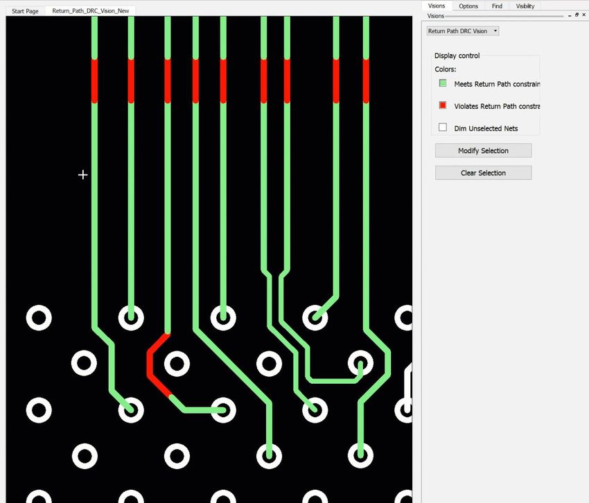
Allegro Design Entry HDL

• Control replacement of a part with specific parts only
    – User defines property on component instances which defines allowed alternate (approved)
      components
    – Property name can be configured using project (cpm) file directive

• Generation of Intel Schematic Connectivity Format (ISCF)
    – Generate Netlist format defined by Intel for schematic validation
    – Configuration options available for defining
         – Property list, Power & Ground nets, and Log file location

• Compatible footprint check in Variant Editor
    – Ensures only parts which have compatible footprints can be used for Replace
    – Compatible footprints are those which have same JEDEC_TYPE / ALT_SYMBOLS or defined
      in compatible JEDEC Type file
    – This check existed before as a warning; now it is a strict check
4     © 2018 Cadence Design Systems, Inc. All Rights Reserved Worldwide.
Allegro SDA improvements
Introduced after QIR5, before QIR6                                         Mass editing of variant data

• Variant Spreadsheet Editor (EAP) for mass
  editing of variant data
    – Available through an environment variable

• Creation of SDA project from a
  DE-HDL project

• Availability of signal list at time of naming /
  rename signals of a blocks
    – Drop down list filters available signal names as you
      type

5     © 2018 Cadence Design Systems, Inc. All Rights Reserved Worldwide.
Allegro SDA - Navigation Links (EAP)
Introduced in an ISR after QIR5, before QIR6
                                                                               Page#, zone
• Signal navigation aid used for
  tracing signals while reviewing
  design in SDA / PDF / print-outs

• Navigation links are hyperlinked
  for quick navigation
    – Contains page number and zone
      information of target
    – Zone information read from Cref
      Data File which can be configured
      using a Project (cpm) file directive                                 OffPage / Port symbols connected to nets are used for
                                                                                       generation of navigation links

6     © 2018 Cadence Design Systems, Inc. All Rights Reserved Worldwide.
Allegro SDA improvement in QIR6
Smart PDF – enabled through Design Publisher license
• Save as pdf (available before)
    – Black & White
    – Color
    – Searchable, but no intelligence

• Smart PDF provides
    –   Hierarchy view
    –   Thumbnail view
    –   Object Model view*
    –   Support for Table objects as searchable objects (ISR#39, May 11th)

• Not supported yet
    –   Security features
    –   Attribute filtering (control what shouldn’t be passed to pdf)
    –   PDF / A
    –   Watermark
    –   Page Setup
7                                                                       *:
        © 2018 Cadence Design Systems, Inc. All Rights Reserved Worldwide.   available only through Acrobat reader
Allegro SDA – QIR6
Ultra Librarian Integration
• Ultra Librarian provides easy
  access to starter libraries
    – Subscription service from
      EMA Design Automation (required)

• Provides search capability for
  parts coming from multiple
  vendors
    – Allow Preview & download of
      Symbols, Footprints and
      3D Models
    – Selected part can also be placed
      directly in SDA

8     © 2018 Cadence Design Systems, Inc. All Rights Reserved Worldwide.
Allegro SDA improvements
ISRs after QIR6
• Performance Improvements (ISR#39, May 11th)
    – Import/Re-Import SDA

• UX improvements (ISR#39, May 11th)
    – Dark Theme issues fixed
    – New dynamic zoom mode
         – Click control and middle mouse button
         – Zoom out by moving mouse down
         – Zoom in by moving mouse up

• Import Capture Design (ISR#40, May 25th)
    – Support for hierarchical designs
    – Support for capture.ini
    – (Capture import introduced in QIR5 – Dec 2017)

9     © 2018 Cadence Design Systems, Inc. All Rights Reserved Worldwide.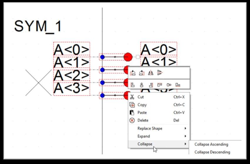
Allegro Library Authoring tools
     What’s new in QIR6

10    © 2018 Cadence Design Systems, Inc. All Rights Reserved Worldwide.
Allegro PCB Librarian – New Symbol Editor
• First introduced in 17.2-QIR3
• Single location for editing logical pin
names and physical pin numbers
– Spreadsheet view in Symbol Editor allow
editing of Pin Numbers and Pin Types
– Edited data is written to package section
(chips.prt file) on symbol save
– Removes need for capturing this information
in Package View
• Add multiple scalar pins in single
operation
– Multiple scalar pins can be added in a single
operation
– Add six pins by specifying A5-A0
11 © 2018 Cadence Design Systems, Inc. All Rights Reserved Worldwide.Allegro PCB Librarian – New Symbol Editor (contd.)
Vector bus can be expanded
into individual bus bits
Individual bus bits can be
collapsed into Vector bus
12 © 2018 Cadence Design Systems, Inc. All Rights Reserved Worldwide.What’s new in Allegro PCB layout and routing
QIR6
13 © 2018 Cadence Design Systems, Inc. All Rights Reserved Worldwide.What’s new in Allegro PCB layout and routing in QIR6 • Allegro® DesignTrue™ DFM • Allegro PCB Symphony Team Design – Real time co-design • MCAD-ECAD and interactive 3D Canvas • Integrated analysis for critical high-speed signals • Productivity boosters 14 © 2018 Cadence Design Systems, Inc. All Rights Reserved Worldwide.
Typical DFM / NPI process
                      • Unnecessary iterations with the manufacturing partners
                      • Lots of pressure because it is the LAST step before the product can be built /
                        shipped
D
     H
E                Placement                    Routing               Batch          Fix       Batch
     O
S                                                                   DFM                      DFM                                     Fix Errors
I
     U            Routing                     Mfg Prep              Check         errors     Check
     S
G
     E
N
                                                                                                                            TQs
                                                 TQs*
                                                                                                                          (Errors)
                                                (Errors)

         P                                                                                                      Complete                                    Final
         A      Preliminary
                DFM check                                                                                      DFM Check                                  DFM Check
M        R
F        T
G        N
         E
         R
                                                                                                                               Time – function of board
                             >3 days                                                                            ~1 week
                                                                                                                               and list of issue found

    15       © 2018 Cadence Design Systems, Inc. All Rights Reserved Worldwide.
                                                                                   *: TQs: Technical Queries
Challenges with the Typical Process
• Unnecessary iterations with the manufacturing partner
• Time to fix errors takes too long, or same errors keep coming back with every
design
• Sometimes manufacturers make – what they think – is a minor change
– May lead to undetected signal- / power-integrity issues
– Can lead to unexpected RMAs
– Bad reputation, can affect current and future sales
• Typical issues found
1. Annular ring issues
2. Copper spacing issues
3. Differential pairs that neck down and shouldn’t
4. Void around the via - the traces run right the edge of the cut out
5. Plane issues - vias half in half out
6. Backdrilling issues – spacing checks of drill hole to metal, annular ring metal remaining?
16 © 2018 Cadence Design Systems, Inc. All Rights Reserved Worldwide.NPI Process with Allegro PCB DesignTrue DFM
Manufacturing rules-driven design
• Allegro® PCB DesignTrue DFM
provides
– DFF and DFA rules
Batch
D Placement Routing
DFM – Over 2000 advanced checks
H Routing Mfg Prep
E
O
Check independent of electrical rules
S Allegro PCB DesignTrue DFM
I
U
S • Real-time checks as you design
G
N
E Design
data
– Signoff with confidence
– Save at least one day per
iteration
P
Final
A DFM Rules DFM Check Mfg • Ensures design is ready for
M R
F T manufacturing
G N
EDesign for Manufacturing Checks All areas of PCB fabrication and assembly are covered • Etching • Lamination • Drilling • Plating • Solder masking • Silk screening • Assembly 18 © 2018 Cadence Design Systems, Inc. All Rights Reserved Worldwide.
Design for Fabrication (DFF) Checks (introduced in 17.2-QIR4)
Complete list of checks
                                                                                                 TH Pin to TH Pin (Y)
                                                                                             Y
• Outline
• Mask                                                               TH Pin to SMD Pin   X

• Annular ring
•    Copper spacing                                                                          Z
                                                                                                                Trace too close to a cut-out       Silkscreen to silkscreen
•    Silkscreen                        SMD Pin to SMD Pin
                                                                                                                                                       Silkscreen to pad

•    Holes
•    Copper features
•    Back-drilling
•    Analytics (ex. hole aspect ratio)
                                                                                                      Acid trap in a shape                       Solder paste wicking
•    Rigid-flex features (ex. arc corner)                                                                                                 Maximum exposed etch in soldermask

19       © 2018 Cadence Design Systems, Inc. All Rights Reserved Worldwide.
Design for Assembly (DFA) Checks (QIR6)
Extensive checks for assembly process
• Outline checks Conveyed Edge
– Component to board outline* Component to board outline
North-South or East-West
– Tall component conveyed edge (board outline) Conveyed Edge
– High pin-count component to board outline
Conveyed Edge PCB PCB
• Component checks North-South East-West
– Component pin to component body*
– Edge finger to component body
– Mechanical hole to component body*
– Via under a small outline component
– Trace under a small outline component
• Fiducial checks
– Fiducial to component body
– Number of fiducials per footprint
– Inside/outside body location checks Component pin to Trace / via under
component body a small outline component
• Pastemask checks*
– Pastemask to outline / cutout check
– Pastemask to pastemask check
– Pastemask to via pad check
– Pastemask size to SMD pad size
– Missing pastemask for SMD pins
– Pastemask to soldermask pad ratio
– Pastemask to coverlay pad ratio Pastemask to soldermask
Pastemask to Board Outline Pastemask to cutout
Pastemask to SMD Pad size or coverlay pad ratio
20 *: Core checks
© 2018 Cadence Design Systems, Inc. All Rights Reserved Worldwide.
All other checks: advanced checksNew DFA Board Outline / Cutout Checks
• Component outline to board outline check*
– Min spacing for board outline or cutout to component
– Exclude certain class of components
– Edge connectors
– Mechanical symbols that overhand the board outline
• Special conveyed edge outline to component
checks
– North-south or east-west conveyed edge assignment Conveyed Edge
– Tall component to conveyed edge
– User-defined minimum height for a tall component
Conveyed Edge PCB
– Tall component to conveyed edge minimum spacing PCB
• Minimum board outline to high pin-count North-South East-West
component spacing check
– User defines minimum pin-count number for high pin
component types
*: Core checks
21 © 2018 Cadence Design Systems, Inc. All Rights Reserved Worldwide.Allother checks: advanced checksNew DFA Spacing Checks
• Component pin to other component body*
– Minimum pin to component body spacing
– SMD pin minimum spacing
– Thru pin minimum spacing
– Edge finger to other component body minimum
spacing
– Fiducial to component other body spacing
• Mechanical hole to body minimum spacing*
• No via and no trace under small outline
component check
– Based on user-defined list of symbols
*: Core checks
22 © 2018 Cadence Design Systems, Inc. All Rights Reserved Worldwide.
All other checks: advanced checksNew DFA Fiducial Checks • User-defined list of symbols that require fiducials • Number of fiducials required for each symbol • Inside/outside of body fiducial location requirements 23 © 2018 Cadence Design Systems, Inc. All Rights Reserved Worldwide.
New DFA Pastemask Checks*
• Pastemask to outline / cutout check

• Pastemask to pastemask check                                                                                 Pastemask to Board Outline       Pastemask to cutout

• Pastemask to via pad check

• Pastemask size to SMD pin pad size
                                                                                                                                            Pastemask to soldermask
• Check for SMD pins missing pastemask                                                                         Pastemask to SMD Pad size      or coverlay pad ratio

• Pastemask size to other mask pad type sizes
     – Pastemask pad to soldermask pad
     – Pastemask pad to coverlay pad
                                                                           *: Core checks
24    © 2018 Cadence Design Systems, Inc. All Rights Reserved Worldwide.
                                                                           All other checks: advanced checks
What’s new in Allegro PCB layout and routing in QIR6 • Allegro® DesignTrue™ DFM • Allegro PCB Symphony Team Design – Real time co-design • MCAD-ECAD and interactive 3D Canvas • Integrated analysis for critical high-speed signals • Productivity boosters 25 © 2018 Cadence Design Systems, Inc. All Rights Reserved Worldwide.
Allegro PCB Symphony Team Design Option
Concurrent design with shared canvas

                                                                          • Multiple PCB designers access a
                                                                            common PCB layout database

          80 %                                       % time spent on
                                                   routing designs with   • Everyone co-designs together in real
                                                     medium to high
                                     10 %              complexities         time

                     Placement, routing, testability, DRCs                • Easy setup eliminates copy/paste
                                                                            database “chaos”
                   Reduce total PCB design time by up to 70%
                       (8 engineers working in parallel)

26   © 2018 Cadence Design Systems, Inc. All Rights Reserved Worldwide.
Allegro Symphony Team Design
New in QIR6
• Z-Copy & Bounding Shape support
• 3D visualization while connected to a session
– Dynamic Rigid-Flex Bending / Cutting Planes, Collison
Checking
– Solder Mask and Silkscreens generation
• Client cursor location and tracking
– “Color Coded” crosshair tracks client movement
– Center display on a specific client cursor
• Performance improvement with server acceptance
of shape updates
27 © 2018 Cadence Design Systems, Inc. All Rights Reserved Worldwide.Feedback from Customers on Symphony
• “Symphony is the best thing that has happened to Allegro® since PCB Team Design was
introduced”
• “Working with Symphony on this design made it possible for us to shrink the time schedule
with 4 weeks. My guess is that 3 of the weeks could be cut purely due to us three layout
designers being able to work in parallel most of the time”
• “Symphony will change our way of working. The possibility of gathering layout resources
will make the design cycle shorter than before. Sometimes we are waiting on schematic
designers to finish their work, and I can very easy jump in and help my colleagues in a
Symphony session instead”
• “Symphony is very easy to use”
• A large customer in China has reported using Symphony on 40 boards with great success
– 80K pin High speed / high density actual design was finished using symphony within record
breaking time
– Symphony was able to let us maximize our engineers time to increase productivity.
28 © 2018 Cadence Design Systems, Inc. All Rights Reserved Worldwide.What’s new in Allegro PCB layout and routing in QIR6 • Allegro® DesignTrue™ DFM • Allegro PCB Symphony Team Design – Real time co-design • MCAD-ECAD and interactive 3D Canvas • Integrated analysis for critical high-speed signals • Productivity boosters 29 © 2018 Cadence Design Systems, Inc. All Rights Reserved Worldwide.
MCAD-ECAD and 3D interactive canvas

• Interactive 3D Canvas improvements

• STEP model support improvements

• Allegro ECAD MCAD Library Creator improvements

30   © 2018 Cadence Design Systems, Inc. All Rights Reserved Worldwide.
PCB Editor

3D Interactive Canvas – QIR6

• Native 3D interactive canvas
     – Eliminate unnecessary ECAD-MCAD
       iterations
     – Continuous improvements in every QIR
       since April 2016
• Shadowing
     – Shadows cast on components and
       beneath the board for more realistic view
• Centering
     – Image automatically centers on canvas
       after any bending operations
• Symbol representation update
     – Two additional options added

31     © 2018 Cadence Design Systems, Inc. All Rights Reserved Worldwide.
PCB Editor
STEP model support improvements
• Purge STEP model mapping
– Removes STEP model mapping to all package symbols in
current drawing
– Maintains housing and mechanical model STEP mapping
• Ignore mapped STEP model for package symbol
during export
– Uses PLACE_BOUND with height property for export in
place of STEP model.
• Refresh STEP models mapped to symbols
32 © 2018 Cadence Design Systems, Inc. All Rights Reserved Worldwide.Allegro ECAD-MCAD Library Creator – S004 Release
• Library Creator Server
– Vastly improved installation process
– True Windows self-extracting installer with self-guiding dialog
– New web interface for administration of accounts, users, permissions and groups
– System dataset integrated with server distribution
– Server now installed as a “system service” for both Windows and Linux
• Library Creator Client
– Client permissions now obtained from server
– New centering modes added to 'Change ECAD Origin' tool
– Added 'Letter' based numbering to sequence tools and remember settings for naming tools
Expression support in naming tools has been replaced with drop-down UI options
– New pin naming tool based on sequential user picks
– Added type tag menus to 'Mounts' and 'Others' when performing direct feature assignment from
the model tree.
33 © 2018 Cadence Design Systems, Inc. All Rights Reserved Worldwide.What’s new in Allegro PCB layout and routing in QIR6 • Allegro® DesignTrue™ DFM • Allegro PCB Symphony Team Design – Real time co-design • MCAD-ECAD and interactive 3D Canvas • Integrated analysis for critical high-speed signals • Productivity boosters 34 © 2018 Cadence Design Systems, Inc. All Rights Reserved Worldwide.
Allegro PCB
                                                                            High Speed Option
Return Path Checking (QIR4)
Save a lot of time manually checking

• Specify reference planes for
  critical nets in Constraint Manager
     – Above or below or both
     – Reference nets, layer

• Looks for deviations
     – Ignore certain length deviations
     – Ignore max pad gap

• Save time screening for signals without
  reference ground / power planes

• Eliminate unnecessary iterations with SI/PI
  engineers
35     © 2018 Cadence Design Systems, Inc. All Rights Reserved Worldwide.
Allegro PCB
High Speed Option
Return Path Design Rule Check (DRC) Update (QIR 5)
Online return path DRC
• Ensure proper reference plane adherence
and detection of signals crossing voids
• New analysis mode allows dynamic
generation of DRCs as changes are made
Enhanced Return Path DRC Vision Display
• Segment color coding reflecting return path
constraint being met or violated
• Trace or Shape adjustments will
dynamically update color coding so a
passing result can be easily seen
– No need to display adjacent layers or DRCs
36 © 2018 Cadence Design Systems, Inc. All Rights Reserved Worldwide.Allegro PCB
High Speed Option
Return Path DRC Enhancements (QIR6)
• Stitching via constraint
defines valid radius
from center of signal via
Signal Path
• Checks for Return Path
– Existence of stitching via
– Distance of stitching via from
signal via
37 © 2018 Cadence Design Systems, Inc. All Rights Reserved Worldwide.What’s new in Allegro PCB layout and routing in QIR6 • Allegro® DesignTrue™ DFM • Allegro PCB Symphony Team Design – Real time co-design • MCAD-ECAD and interactive 3D Canvas • Integrated analysis for critical high-speed signals • Productivity boosters 38 © 2018 Cadence Design Systems, Inc. All Rights Reserved Worldwide.
DE-HDL : PCB Editor

Schematic Driven Placement

                             HDL Symbol Locations                                 Allegro Footprint Locations

 • Enables users to Quickplace components by schematic symbol locations
     – Footprint locations can be condensed or spread out through a user adjustable scaling factor
 • Proper schematic symbol placement can now be used to pass along rough
   placement intent to designers

39   © 2018 Cadence Design Systems, Inc. All Rights Reserved Worldwide.
                                                                          Video
PCB Editor
Reuse module with different stack-up than the original design
Place Replicate Enhancements
• Modules can now be re-used with
differing or larger stack-ups
– Drag & drop mapping of modules to new
stack-ups
– Replication of non-etch & unconnected
elements
– Regions, text, lines, keepouts, etc.
Original – HDI vias will adjust to keep connectivity
module – Embedded component layers can be
designed
on 4 layers
mapped to other embedded layers
• Additional supported objects
Reuse
– Dummy net objects
on – Floating clines, vias, shapes, etc.
18 layer
design – Text, line, and non-etch shape elements
– Constraint regions
40 © 2018 Cadence Design Systems, Inc. All Rights Reserved Worldwide.PCB Editor
Additional Improvements
• Copy/Paste Update
– The “Paste” operation now supports a “Retain net of shapes” option that will retain the original
net of the shape being pasted
– Alternatively, it can allow net name to be inherited by the destination object
– The default setting preserves current default behavior
• Basic PDF Export
– Available to all OrCAD and Allegro PCB Editor products, a non-intelligent PDF Export command
provides a method to print 2D PDF without tree structures and meta data
– This version of PDF Export becomes available if the PDF Publisher license is not found
41 © 2018 Cadence Design Systems, Inc. All Rights Reserved Worldwide.© 2018 Cadence Design Systems, Inc. All rights reserved worldwide. Cadence, the Cadence logo, and the other Cadence marks found at www.cadence.com/go/trademarks are trademarks or registered trademarks of Cadence Design Systems, Inc. All other trademarks are the property of their respective owners.
You can also read