Wireless Enhanced Electrochemiluminescence at a Bipolar Microelectrode in a Solid-State Micropore - IOPscience
←
→
Page content transcription
If your browser does not render page correctly, please read the page content below

Journal of the Electrochemical
Society

OPEN ACCESS

Wireless Enhanced Electrochemiluminescence at a Bipolar
Microelectrode in a Solid-State Micropore
To cite this article: Silvia Voci et al 2020 J. Electrochem. Soc. 167 137509

View the article online for updates and enhancements.

                                This content was downloaded from IP address 46.4.80.155 on 03/12/2020 at 07:41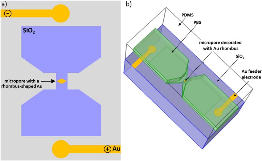
Journal of The Electrochemical Society, 2020 167 137509

                               Wireless Enhanced Electrochemiluminescence at a Bipolar
                               Microelectrode in a Solid-State Micropore
                               Silvia Voci,1,= Abdulghani Ismail,2,= Pascale Pham,3 Jing Yu,1 Ali Maziz,4
                               Fabien Mesnilgrente,4 Lucile Reynaud,2 Thierry Livache,2 Pascal Mailley,3 Arnaud Buhot,2
                               Thierry Leichle,4,5 Alexander Kuhn,1 Loic Leroy,2 Aurélie Bouchet-Spinelli,2,z and
                               Neso Sojic1,z
                               1
                                 Univ. Bordeaux, Bordeaux INP, ISM, UMR CNRS 5255, 33607 Pessac, France
                               2
                                 Univ. Grenoble Alpes, CEA, CNRS, IRIG, SYMMES, F-38000 Grenoble, France
                               3
                                 Univ. Grenoble Alpes, CEA LETI, F-38000, Grenoble, France
                               4
                                 LAAS-CNRS, Université de Toulouse, 31400 Toulouse, France
                               5
                                 Georgia Tech-CNRS Joint International Laboratory, School of Electrical and Computer Engineering, Atlanta, GA, United
                               States of America

                 The combination of bipolar electrochemistry (BE), as a wireless electrochemical approach, and of electrochemiluminescence
                 (ECL) as an imaging readout is a successful strategy with a wide range of analytical applications. However, small conductive
                 entities such as micrometric and nanometric objects are particularly difficult to polarize by BE since they require extremely high
                 electric fields. In order to circumvent this issue due to intrinsic limitations of BE, we elaborated a solid-state micropore, decorated
                 with a rhombus-shaped gold microelectrode. The electric field strength was concentrated inside the solid-state micropore where the
                 conductive gold microelectrode was precisely located and acted as a bipolar light-emitting device. This original configuration
                 allowed achieving adequate polarization of the gold microelectrode in a wireless manner, which led locally to ECL emission. ECL
                 imaging shows that light was generated by the bipolar microelectrode in the center of the micropore. ECL emission could be
                 achieved by imposing a potential value (10 V) to the feeder electrodes that is more than 2 orders of magnitude lower than those
                 required without the micropore. The reported ECL approach opens exciting perspectives for the development of original wireless
                 bioanalytical applications and dynamic bipolar experiments with small objects passing through the pores.
                 © 2020 The Author(s). Published on behalf of The Electrochemical Society by IOP Publishing Limited. This is an open access
                 article distributed under the terms of the Creative Commons Attribution 4.0 License (CC BY, http://creativecommons.org/licenses/
                 by/4.0/), which permits unrestricted reuse of the work in any medium, provided the original work is properly cited. [DOI: 10.1149/
                 1945-7111/abbbc1]

                 Manuscript submitted August 9, 2020; revised manuscript received September 24, 2020. Published October 7, 2020. This paper is
                 part of the JES Focus Issue on IMCS 2020.
                 Supplementary material for this article is available online

    Electrochemiluminescence (ECL) is a sensitive analytical tech-                     straightforward way. In BE, the electrochemical addressing of
nique, which is widely applied in analytical chemistry for the                         conducting objects is achieved without physical connection to a
detection of clinical biomarkers, biological warfare agents and                        power supply through an electric contact.34–36 In the most common
foodborne pathogens, as well as for microscopy of cells, micro/                        “open” configuration, two feeder electrodes are connected to a
nanoparticles and electrochemical processes.1–4 The light emission                     power supply and immersed in an ionically conducting media. An
results from an initial electrochemical step. It involves a light-                     electronically-conducting object is positioned in solution in the
emitting species, the luminophore, and a sacrificial coreactant                         electric field generated by both feeder electrodes. In a first order
species, whose role is to provide highly energetic radicals upon                       approximation, the electric field can be considered as a linear
electrochemical reactions. ECL starts with a heterogeneous electron-                   potential drop across the solution. As the conductive object is by
transfer reaction at the electrode surface, continues with a cascade of                definition at an equipotential value, an interfacial polarization
homogeneous reactions with a coreactant species, which produces                        potential is established alongside the object.37,38 When the potential
the excited state of a luminophore, and ends with photon emission.                     drop and thus the resulting polarization potential is high enough, the
Most of the analytical applications in aqueous media rely on the use                   object acts as a bipolar electrode with cathodic and anodic features at
of ruthenium(II) tris(bipyridine), [Ru(bpy)3]2+, and tri-n-propyla-                    its two extremities. This triggers simultaneously reduction and
mine (TPA) as the luminophore and the coreactant, respectively.5,6                     oxidation reactions at its surface with the cathodic and anodic poles
This tandem model system is highly efficient and generates bright                       facing the feeder anode and cathode, respectively. In other words,
emission. In ECL, the analytical information is contained in the light                 different electrochemical processes occur concomitantly at the
signal and its intensity is directly proportional to the concentration of              surface of the bipolar object. Thanks to its intrinsic features (i.e.
a limiting reactant (typically, the luminophore or the coreactant)                     wireless, duality of the redox reactions, gradients of electrochemical
involved in the ECL process. ECL combines thus intimately the                          reactivity), BE has attracted in the last few years an exponentially
initial electrochemical stimulation and the final optical signal. ECL                   increasing interest in different fields.39–44 Since ECL combines
has been used to image various electrochemical processes,7–9                           electrochemical addressing and orthogonal optical readout, it com-
surfaces10–12 or objects13,14 as well as cells.15–21 ECL was also                      plements very efficiently with BE. Indeed, the optical output of ECL
investigated in various confined configurations.7,10,11,22–24                            may reflect the electrochemical reactivity of the bipolar objects in
    In the last decade, ECL was successfully combined with bipolar                     different configurations as initially demonstrated by Manz and
electrochemistry (BE) because it is a wireless electrochemical                         Crooks.25,45 The combination of ECL and BE has been successfully
technique.25–33 Indeed, due to this contactless nature, classical BE                   applied mainly in analytical chemistry, for the measurement of
setups do not allow to measure directly an electrochemical signal                      different biomolecules using various detection strategies, as well as
reflecting the reactivity of the investigated conductive object in a                    for the development of dynamic ECL “swimmers”.31,46–50 However,
                                                                                       addressing micrometric or nanometric objects by BE remains a
                                                                                       difficult task, because it requires high electric fields. Indeed, the
  =
                                                                                       shorter the conducting object (more precisely, the effective length
      These authors contributed equally to this work.
  z
      E-mail: Aurelie.Bouchet-Spinelli@cea.fr; Neso.Sojic@enscbp.fr
                                                                                       along the axis parallel to the electric field vector), the larger is the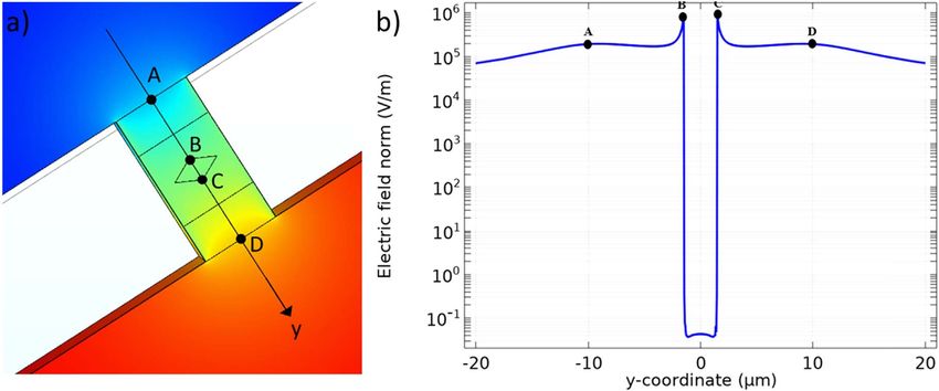
Journal of The Electrochemical Society, 2020 167 137509

electric field required to polarize it in order to induce both                    which focuses the potential drop (ii) a bipolar microelectrode that
electrochemical reactions at its poles.34 Therefore, this drawback               emits ECL light in a wireless manner. Using this set-up, we were
for polarizing small objects due to the inherent physical features of            able to polarize a microelectrode, which is almost 7-times shorter
BE represents a challenging issue which needs to be overcome.51                  than the length of the micropore, with a very low potential difference
    One of the main factors governing BE is the potential drop across            (10 V). Finally, the localized potential drop was rationalized by finite
the solution.34 Therefore, shaping the spatial distribution of the               element simulations.
potential drop may open new perspectives for BE. The spatial
confinement of this potential drop has been achieved using micro-                                               Experimental
pore and nanopore technology.52–55 Indeed, a sharp potential drop
                                                                                    Chemicals.—All chemicals were obtained from Sigma-Aldrich
can be generated at the level of such spatial restrictions. Modified
                                                                                 except SU-8 2075, which was purchased from Michrochem. Tris
nanopipettes have been used to detect various analytes by BE or
                                                                                 (2,2′-bipyridyl)dichlororuthenium(II) hexahydrate and tri-n-propy-
ECL.52,56–58 For example, Long et al. described the detection of
                                                                                 lamine were prepared in phosphate buffer solution (0.1 M, pH 7.4).
NADH in living cells using an asymmetric nanopore electrode with a
                                                                                 The conductivity of the solution was 13.9 mS cm−1.
diameter down to 90 nm.56 The potential drop was focused at the
nanopore electrode, which converts the faradaic current into a
                                                                                     Fabrication of silicon microchips with an integrated micro-
bubble-induced transient ionic current. Zhang et al. reported the
                                                                                 pore.—The micropore chips were fabricated using top-down micro-
measurement of single nanoparticles passing through a bipolar
                                                                                 machining (Fig. 2) onto 100 mm n-type silicon substrates (ρ < 0.01
nanopore.40,59 Jiang et al. modified the internal walls of a nanopip-
                                                                                 Ω cm) cleaned by oxygen plasma in a Diener machine (800 W,
ette tip with Pt to perform wireless ECL analysis of single living
                                                                                 5 min) prior processing. The micropore patterns were transferred
cells.60 Recently, we reported solid-state micropores for bipolar
                                                                                 onto the silicon wafers by a photolithography step followed by
ECL.61 We used a deoxidized silicon 20-μm long path to demon-
                                                                                 reactive ion etching for a total depth of 20 μm. Photolithography was
strate its wireless polarization and ECL emission.
                                                                                 performed with spin-coated positive photoresist ECI 3012 2.5 μm
    Herein, we extend this approach based on solid-state planar
                                                                                 and the micropatterns were etched in the silicon using SF6 (250
micropores61 by integrating a rhombus-shaped (dimensions: 6 ×
                                                                                 sccm), C4F8 (250 sccm), and O2 (35 sccm). The plasma source was
3 μm) Au microelectrode in a microfluidic channel (Fig. 1). The goal
                                                                                 generated by an inductively coupled plasma source manufactured by
was to demonstrate the possibility to address a single conductive
                                                                                 Alcatel Comptech Inc. The residual photoresist layer was removed
object located in the micropore. A Au microelectrode was precisely
                                                                                 by acetone and O2 plasma (800 W, 5 min). Then, dry thermal
fabricated in the middle of the micropore, in the region where the
                                                                                 oxidation was performed in a furnace to grow 300 nm of SiO2
highest potential drop occurs. ECL was generated using the model
                                                                                 onto the silicon wafers. Finally, metal electrodes were patterned on
[Ru(bpy)3]2+/TPA system at very low potentials considering the
                                                                                 the SiO2 layer by photolithography and wet etching. Briefly, a layer
effective length of the rhombus-shaped Au microelectrode along the
                                                                                 of Ti/Au of 50 nm/200 nm was first deposited by physical vapor
axis of the electric field vector (i.e. 3 μm). Oxidation of the ECL
                                                                                 deposition using a Univex 450 C and etched in appropriate baths
reagents at the anodic pole of the bipolar electrode leads to strong
                                                                                 after carrying out photolithography with the positive photoresist AZ
ECL signals. ECL imaging shows that emission occurs in the middle
                                                                                 4999. The wafers were finally diced into 20 mm × 20 mm chips,
of the micropore at the level of the bipolar Au microelectrode. The
                                                                                 each one containing a single micropore.
fabricated device comprises two features: (i) a spatial restriction,

Figure 1. Schematic representations of the silicon microchip integrating the solid-state micropore, which was decorated with a rhombus-shaped bipolar Au
electrode (yellow color). Top view (a): The Au feeder electrodes (yellow color) are shown. 3D view (b): the silicon microchip was covered with a PDMS mold
(transparent color) that was specifically designed in order to define a microfluidic channel filled with the PBS solution (green color) and the ECL reagents. The
top view scheme (a) is not to scale, the 3D view (b) is to scale.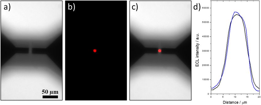
Journal of The Electrochemical Society, 2020 167 137509

Figure 2. Fabrication process flow of the silicon microchip. Cross section view along the middle of the micropore. (a) Micropore fabrication on the silicon wafer
by photolithography followed by reactive ion etching. (b) Dry thermal oxidation of the silicon wafer to grow 300 nm of SiO2. (c) Patterning of feeder Au
electrodes and the rhombus-shaped Au surface by photolithography and wet etching techniques. (d) Encapsulation of the microfluidic channel in a molded PDMS
slab and filling the fluidic channel with PBS solution. The scheme is not to scale.

    SU-8 on silicon mold was fabricated by a conventional photo-                   was amplified by a Keithley 6485 Picoammeter before acquisition
lithography process in order to prepare the PDMS channels (Fig. 1b).               via the second input channel of the PGSTAT30 Autolab potentiostat.
Briefly, a 4-inch silicon wafer was sonicated for 5 min in acetone                      Potential pulses of 10 V with z duration of 300 ms and separated
then in isopropranol (IPA). It was then dried at 180 °C for 15 min                 by a delay of 100 ms were applied for 10 s using a DG1032 power
and SU-8 2075 negative photoresist was spin coated for 5 s at                      supply from Rigol. ECL images were recorded using an epifluores-
500 rpm followed by 30 s at 2000 rpm then another 5 s at 500 rpm.                  cence Leica (DMI6000, Leica Microsystems) microscope equipped
The acceleration was always 300 rpm s−1. Following this, soft                      with an EM-CCD 9100–13 camera from Hamamatsu. All experi-
baking at 65 °C for 5 min then 95 °C for 20 min, and finally 65 °C                  ments were performed at ambient temperature (25 °C). Exposure
for 5 min was applied. The design of the channels was drawn using                  time of the CCD camera was synchronized with the potential
KLayout. It was directly written on the resist via laser photolitho-               application for 10 s. The images were treated using Image J
graphy (70 mW, 70%) (μPG 101 Heidelberg Instrument, Germany)                       software.
followed by a post exposure bake (PEB) at 65 °C for 2 min then 95 °                    SEM images were obtained with a FEI Helios 600i SEM
C for 8 min. The unexposed parts of the resist were removed by                     instruments.
developing in SU-8 developer for 10 min then in IPA for 30 s. In
order to make the SU-8 motifs very resistant, a hard bake at 150 °C                    Finite element simulation.—To study the electrochemical beha-
for 15 min was carried out. The height of the channel (140 μm) was                 vior of the micropore with an integrated bipolar microelectrode,
characterized with a profilometer (Dektak DXT “E”, USA).                            finite element simulations were performed using the Finite Element
    The chips were finally capped with a PDMS microfluidic                           code Comsol Multiphysics™, by solving Maxwell’s equations using
channel62 by pouring a mixture of elastomer and curing agent at a                  the Static and Low-Frequency Electromagnetics module (ACDC).63
ratio of 10/1 onto the SU-8 mold after proper degassing. The PDMS                  A simplifying assumption of this numerical model was to consider
was cured at 60 °C for 1 h before demolding. The prepared PDMS                     that no electrochemical double layer was formed at the feeder
and the silicon chips were activated using oxygen plasma and they                  electrodes surface. The potential applied to the Au feeder electrodes
were aligned using a MJB4 mask aligner from Suss MicroTec before                   was −5 and +5 V respectively. The electrical conductivity of the
bringing them together.                                                            saline solution was measured (13.9 mS cm−1). The description of the
                                                                                   finite element model is detailed in the Supporting Information.
   Instrumentation.—Voltammetric and ECL experiments were
performed with a PGSTAT30 Autolab potentiostat connected to a                                              Results and Discussion
conventional three-electrode cell. ECL intensity was measured using
                                                                                      Fabrication of the microfluidic device with the micropore and
a Hamamatsu photomultiplier tube (PMT) R5070A with a
                                                                                   the rhombus-shaped Au surface.—We designed a microfluidic
Hamamatsu C9525 high voltage power supply. The output signal
                                                                                   device comprising the following main components: a planar solid-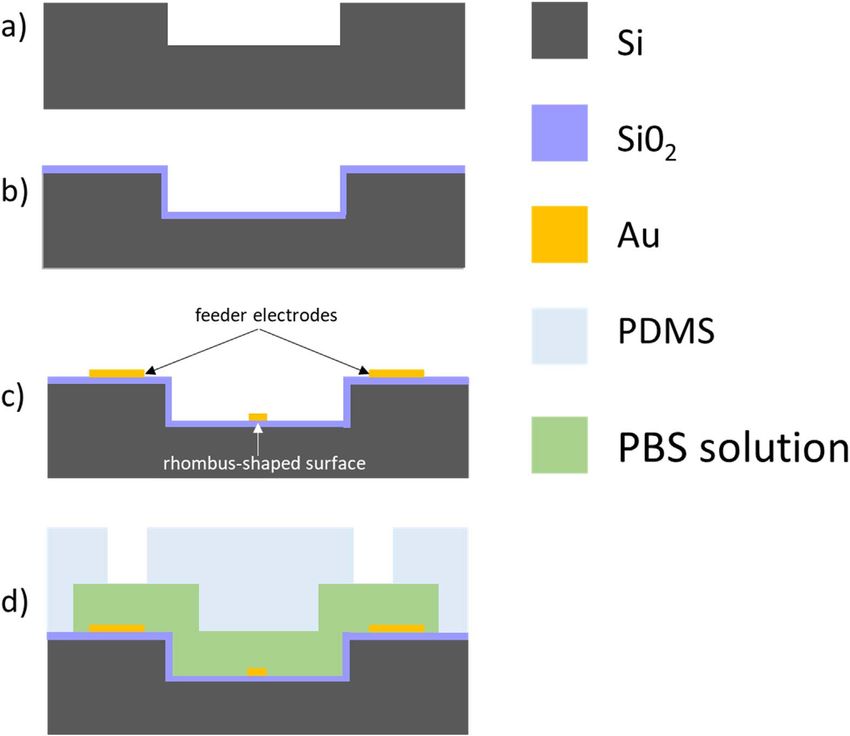
Journal of The Electrochemical Society, 2020 167 137509

state micropore, a single rhombus-shaped Au microelectrode
(without physical connection) and two feeder Au electrodes. These
spatial restrictions are considered as planar because they are at the
surface of the substrate and not drilled through the silicon chips. The
devices were fabricated on 100 mm n-type silicon substrates using
standard micromachining techniques (Fig. 2). Details of the fabrica-
tion process of the solid-state micropore itself have been described
previously.61 However, we modified the fabrication steps to inte-
grate the rhombus-shaped Au surface in the devices (Fig. 2). In the
present work, we added a rhombus-shaped Au microelectrode in the
micropore structure. Briefly, photolithography was first used to
pattern the micropores, consisting of rectangular cavities with a
constriction that was subsequently transferred to the silicon wafer by
reactive ion etching (for a total depth of 20 μm). The SEM images of
the devices were recorded at different magnifications (Fig. 3). They
show the dimensions of the micropore: 20 μm length, 10 μm width
and 20 μm height. After, removing the residual photoresist layer by
acetone and plasma O2, dry thermal oxidation was performed in a             Figure 4. Linear voltammogram (black curve) and ECL signal (red curve)
furnace to grow 300 nm of an insulating SiO2 layer. This layer is           of 1 mM [Ru(bpy)3]2+ in the presence of 50 mM TPA in PBS (pH 7.4)
thick enough to prevent any electrochemical reactions between the           recorded on an Au working electrode at a scan rate of 0.1 V s–1 in a classic 3-
silicon substrate and the ECL reagents dissolved in solution. The Au        electrode setup.
feeder electrodes and rhombus-shaped gold features were fabricated
by first depositing sequentially 50 nm/200 nm Ti/Au layers by                electrode (Fig. 4, black curve). This electrochemical experiment
physical vapor deposition on the oxidized silicon and patterning            has been combined with a simultaneous monitoring of the ECL
the layers by photolithography and wet etching. The wafers were             intensity (Fig. 4, red curve). ECL intensity starts to increase
then diced into 20 mm × 20 mm chips containing a single micro-              significantly at +1 V vs Ag/AgCl/KCl before decreasing rapidly
pore. The two Au feeder electrodes with a radius of 50 μm were              above 1.1 V vs Ag/AgCl/KCl. This decrease is due to the surface
fabricated at the extremities of the chip. The center-to-center             oxide formation on Au in aqueous media, which prevents the
distance d between them was 1.2 mm. The lengths of the short and            efficient oxidation of the amine-based coreactant. The cathodic
long diagonals of the rhombus-shaped Au microelectrode were 6 ×             current (black curve), which corresponds to the reduction of
3 μm, respectively. The chips were finally capped with a PDMS                dioxygen and water increases for potential values below –1 V vs
microfluidic channel created by pouring a mixture of elastomer and           Ag/AgCl/KCl. Considering the value of the anodic current at the
curing agent (Figs. 1b and 2). Since the PDMS is a transparent              potential required to generate ECL, a potential of approximately
material in the visible range, it allowed light transmission during         –1.5 V vs Ag/AgCl/KCl is necessary to obtain a cathodic current of
ECL imaging experiments. These fabrication steps lead to a                  the same intensity. Therefore, a minimal polarization potential
microfluidic device with a solid-state micropore, which integrates           difference ΔVBE of 2.6 V is required for coupling both reactions
a rhombus-shaped Au bipolar microelectrode.                                 on a Au surface in the bipolar configuration.
                                                                                In a classical BE configuration, the polarization potential ΔVBE
   Bipolar electrochemical properties.—To generate ECL in the               induced on a conducting object is proportional to the external
bipolar configuration, it is necessary to estimate the potential             electric field (ΔVFE/d) and the effective length l of the object along
required to oxidize the ECL reagents as well as the potential of            the axis aligned to the electric field vector, as described by the
the reduction reaction. The latter one has to counter-balance the           simple equation:
charge resulting from the reaction on the other pole of the bipolar
electrode. Indeed, the rate of the oxidation reaction has to be equal to                                          DVFE
the reduction process due to global charge neutrality at the level of                                  DVBE =          xl                               [ 1]
                                                                                                                   d
the bipolar electrode. The polarization ΔVBE required to generate
both faradaic reactions at the Au surface was estimated by recording        with ΔVFE being the potential difference applied between the two
the linear voltammetric signals at a conventional Au working                feeder electrodes.

Figure 3. (a) SEM image of the microchip with the micropore (10 × 10 × 20 μm) and the integrated feeder Au electrodes. (b) Zoom on the ECL-emitting
rhombus-shaped Au surface (6 × 3 μm) positioned at the bottom surface of the micropore.
Journal of The Electrochemical Society, 2020 167 137509
This equation is a first order approximation, which does not take rhombus Au surface. The short axis of the rhombus is parallel to the
into account potential drops at the feeder electrodes due to the longitudinal axis of the micropore whereas its long axis is
electrochemical double layer. Considering that ΔVBE and l are 2.6 V perpendicular to it (Fig. 3). Both curves overlay. The full-width at
and 3 μm, respectively, Eq. 1 states that the electric field has to be at half-maximum for both ECL intensity profiles is ∼8 μm whereas the
least ca. 8.7 kV cm−1. In the present chip with d = 1.2 mm, it would dimensions of the rhombus were 6 μm × 3 μm. In fact, the ECL-
correspond to a potential ΔVFE of 1040 V. This value is coherent emitting region should be even smaller than half of the rhombus-
with a difference potential ΔVFE of 30 kV imposed in classical BE shaped Au surface because reduction of dioxygen and water occurs
(d = 45 cm) to modify 2 μm long carbon nanotubes with Au simultaneously on the cathodic pole of this bipolar element. The fact
deposits (ΔVBE = 0.24 V).51 In brief, ECL emission was achieved at that we were not able to resolve better the size and the shape of the
the rhombus-shaped bipolar microelectrode by imposing a potential rhombus surface by ECL imaging is most probably due to the low
difference of only 10 V to the feeder electrodes (vide infra). This optical resolution resulting from the transmission through the 2.5-
value is more than 2 orders of magnitude lower than potentials millimeter thick PDMS layer covering the microchip. In previous
required without the micropore structure. works,22,23 we investigated also ECL in confined environments. The
ECL patterns were different because light was generated either in the
ECL imaging of the rhombus-shaped bipolar microelectrode.— nanochannel at or the level of the access hole areas depending on the
The ECL mechanism of the model [Ru(bpy)3]2+/TPA system is an annihilation or coreactant modes, respectively.
active area of investigation with several competitive pathways,64,65 To generate ECL, a potential ΔVFE of 10 V was imposed at the
which depends on several experimental parameters (e.g. electrode feeder electrodes. This experimental value is much smaller than the
material, surface hydrophobicity, concentration ratio, pH value, 1040 V value calculated theoretically using Eq. 1 and which is
etc.).66 In the present case, the mechanism involves oxidation of required for a configuration without the micropore structure. This
both ECL reagents, which then react together to produce the excited imposed potential, which is more than 2 orders of magnitude lower
state, [Ru(bpy)3]2+*, and thus, ECL emission. As already men- than the theoretically predicted one in a classic bipolar configuration,
tioned, the passivation of the electrode surface by the growth of an is due to the sharp potential drop focused at the level of the
oxide layer at the potentials required for ECL generation may micropore. Indeed, this spatial restriction leads to enhanced local
decrease the ECL signal by preventing the efficient TPA oxidation. polarization and ECL emission. Finite element simulations were
To avoid this effect, we pulsed rapidly the potential ΔVFE of the performed to study the distribution of the polarization at the level of
feeder electrodes from 0 to 10 V for 300 ms with a rest potential of the bipolar Au microelectrode in the micropore.
0 V for 100 ms. Using lower potential values makes it impossible to
record ECL images at the level of the bipolar Au microelectrode. A Finite element simulations.—As mentioned previously, the
higher potential leads to unstable ECL signals. In other words, spatial distribution of the potential is the pertinent experimental
thanks to the micropore, a potential of 10 V is a good compromise to parameter, which determines the electrochemical reactions, their
produce efficiently ECL at the rhombus-shaped Au surface without rates and their locations at the level of the bipolar electrode.
passivating it. Since silicon is an opaque substrate, which does not Figure 6a shows the electric potential distribution calculated by
allow light transmission, the photoluminescent (PL) and ECL finite element simulations without taking into account the effects of
images have been recorded from the top through the PDMS layer. the electrochemical double layer. It shows that the potential drop is
Figure 5a displays the PL image of the micropore without imposing mostly confined inside the micropore where the bipolar Au rhombus
any external potential to the feeder electrodes. It shows that the microelectrode is positioned. This feature allows polarizing it and
micropore and the microfluidic device were filled with the solution generating ECL at low potential values applied to the feeder
containing the PL-active [Ru(bpy)3]2+ luminophore (and the cor- electrodes. We calculated also the norm of the electric field along
eactant). The excitation light was then turned off and the potential the axis passing through the short diagonals of the rhombus
pulses were applied. Figures 5b–5c reveal that ECL emission is (Fig. 6b). This simulated profile shows that the highest values of
confined in the middle of the micropore where the rhombus-shaped the electric field are located at the extremities of the Au electrode (of
Au surface is located. The ECL image shows a bright spot of light the order of MV m−1), confirming that the gold layer in the pore acts
with a disk pattern. From the ECL images, we extracted the ECL as a bipolar electrode.
intensity profiles along both normal axes passing by the short (blue
curve) and long (black curve) diagonals of the microfabricated
Figure 5. (a) PL, (b) ECL and (c) overlayed images of the ECL-emitting bipolar Au microelectrode confined in the micropore. The rhombus-shaped Au surface
was polarized remotely by the feeder electrodes. The ECL image was recorded in PBS (pH 7.4) containing 1 mM [Ru(bpy)3]2+ and 50 mM TPA by applying a
sequence of 10 potential pulses of 10 V for 0.3 s. followed by 0 V for 0.1 s, respectively. D) ECL intensity profiles along both normal axes along the short (blue
curve) and the long (black curve) diagonals of the rhombus.Journal of The Electrochemical Society, 2020 167 137509
Figure 6. Finite element simulation results (0 Hz): (a) electric potential distribution in the vicinity of the micropore, (b) profile of the norm of the electric field
along the y-axis passing by the short diagonals of the rhombus (i.e. along the middle of the micropore through the Au rhombus layer; A-B-C-D points showed on
Fig. 6a). The image was coded according to a color scale of the potential where red and blue colors represent +5 V and −5 V, respectively.
Conclusions 5. E. Kerr, E. H. Doeven, D. J. D. Wilson, C. F. Hogan, and P. S. Francis, Analyst,
141, 62 (2016).
In summary, an analytical fluidic device comprising a solid-state 6. Y. Yuan, S. Han, L. Hu, S. Parveen, and G. Xu, Electrochim. Acta, 82, 484 (2012).
micropore decorated with a rhombus-shaped Au microelectrode was 7. C. Amatore, C. Pebay, L. Servant, N. Sojic, S. Szunerits, and L. Thouin,
designed and fabricated. The potential drop was confined at the level ChemPhysChem, 7, 1322 (2006).
8. C. M. Pharr, R. C. Engstrom, J. Klancke, and P. L. Unzelman, Electroanalysis, 2,
of the micropore where a microelectrode was precisely positioned. 217 (1990).
This configuration allowed polarizing remotely the rhombus-shaped 9. J. Zhang, J. Zhou, C. Tian, S. Yang, D. Jiang, X.-X. Zhang, and H.-Y. Chen, Anal.
Au microelectrode at very low potentials. Indeed, thanks to the Chem., 89, 11399 (2017).
micropore features, only a potential difference of 10 V needs to be 10. L. M. Moretto, T. Kohls, A. Chovin, N. Sojic, and P. Ugo, Langmuir, 24, 6367
(2008).
imposed between the feeder electrodes to generate ECL, instead of 11. L. M. Moretto, T. Kohls, D. Badocco, P. Pastore, N. Sojic, and P. Ugo,
the 100-fold higher potential theoretically required in a configuration J. Electroanal. Chem., 640, 35 (2010).
without the micropore. The electrochemical addressing was revealed 12. C. J. Miller, P. McCord, and A. J. Bard, Langmuir, 7, 2781 (1991).
using ECL emission of the model [Ru(bpy)3]2+/TPA system. Strong 13. M.-J. Zhu, J.-B. Pan, Z.-Q. Wu, X.-Y. Gao, W. Zhao, X.-H. Xia, J.-J. Xu, and H.-
Y. Chen, Angew. Chem. Int. Ed., 57, 4010 (2018).
ECL light was emitted in the middle of the micropore by the Au 14. A. J. Wilson, K. Marchuk, and K. A. Willets, Nano Lett., 15, 6110 (2015).
microelectrode, demonstrating the wireless polarization. The unique 15. C. Cui, Y. Chen, D. Jiang, J.-J. Zhu, and H.-Y. Chen, Anal. Chem., 89, 2418 (2017).
micropore properties were rationalized by finite element simulations, 16. J. Xu, P. Huang, Y. Qin, D. Jiang, and H.-Y. Chen, Anal. Chem., 88, 4609 (2016).
which showed the electric field distribution. The reported strategy 17. R. He, H. Tang, D. Jiang, and H.-Y. Chen, Anal. Chem., 88, 2006 (2016).
18. G. Valenti et al., J. Am. Chem. Soc., 139, 16830 (2017).
could be extended to elaborate a variety of bipolar ECL devices with 19. H. Ding, W. Guo, and B. Su, Angew. Chem. Int. Ed., 59, 449 (2020).
interesting high-throughput features with parallelized micropores. 20. H. Gao, W. Han, H. Qi, Q. Gao, and C. Zhang, Anal. Chem., 92, 8278 (2020).
Finally, it paves the way to dynamic bipolar experiments for the 21. C. Ma, Y. Cao, X. Gou, and J.-J. Zhu, Anal. Chem., 92, 431 (2020).
ECL detection of micro/nano-objects passing through the pores, 22. H. Al-Kutubi, S. Voci, L. Rassaei, N. Sojic, and K. Mathwig, Chem. Sci., 9, 8946
(2018).
where they might generate ECL transiently during the translocation 23. S. Voci, H. Al-Kutubi, L. Rassaei, K. Mathwig, and N. Sojic, Anal. Bioanal. Chem.,
or modulate the ECL signal by hindering the diffusion of the ECL 412, 4067 (2020).
reagents. 24. C. Ma, L. P. Z. Iii, and P. W. Bohn, Chem. Sci., 6, 3173 (2015).
25. A. Arora, J. C. T. Eijkel, W. E. Morf, and A. Manz, Anal. Chem., 73, 3282 (2001).
26. S. E. Fosdick, J. A. Crooks, B.-Y. Chang, and R. M. Crooks, J. Am. Chem. Soc.,
Acknowledgments 132, 9226 (2010).
27. W. Zhan, J. Alvarez, and R. M. Crooks, Anal. Chem., 75, 313 (2003).
We thank the Agence Nationale de la Recherche (Planarpore 28. M. R. Moghaddam, S. Carrara, and C. F. Hogan, Chem. Commun., 55, 1024 (2019).
ANR-15-CE18-0027). This work has been partially supported by 29. H. Li, L. Bouffier, S. Arbault, A. Kuhn, C. F. Hogan, and N. Sojic, Electrochem.
Labex ARCANE and CBH-EUR-GS (ANR-17-EURE-0003). Commun., 77, 10 (2017).
SyMMES laboratory is part of Labex LANEF program (ANR-10- 30. M. Sentic, S. Arbault, L. Bouffier, D. Manojlovic, A. Kuhn, and N. Sojic, Chem.
Sci., 6, 4433 (2015).
LABX-51-01). This work has also been partially funded by the 31. M. Sentic, G. Loget, D. Manojlovic, A. Kuhn, and N. Sojic, Angew. Chem. Int. Ed.,
European Research Council (ERC) under the European Union’s 51, 11284 (2012).
Horizon 2020 research and innovation program (grant agreement no 32. L. Qi, Y. Xia, W. Qi, W. Gao, F. Wu, and G. Xu, Anal. Chem., 88, 1123 (2016).
741251, ERC Advanced grant ELECTRA). 33. Q. Zhai, X. Zhang, Y. Han, J. Zhai, J. Li, and E. Wang, Anal. Chem., 88, 945
(2016).
34. S. E. Fosdick, K. N. Knust, K. Scida, and R. M. Crooks, Angew. Chem. Int. Ed., 52,
ORCID 10438 (2013).
Alexander Kuhn https://orcid.org/0000-0002-1962-4863 35. G. Loget, D. Zigah, L. Bouffier, N. Sojic, and A. Kuhn, Acc. Chem. Res., 46, 2513
(2013).
Aurélie Bouchet-Spinelli https://orcid.org/0000-0003-1709-785X 36. M. Ongaro, A. Gambirasi, and P. Ugo, ChemElectroChem, 3, 450 (2016).
Neso Sojic https://orcid.org/0000-0001-5144-1015 37. M. Li, S. Liu, Y. Jiang, and W. Wang, Anal. Chem., 90, 6390 (2018).
38. M. Hasheminejad, Y. Fang, M. Li, Y. Jiang, W. Wang, and H.-Y. Chen, Angew.
References Chem. Int. Ed., 56, 1629 (2017).
39. A. L. Dauphin, A. Akchach, S. Voci, A. Kuhn, G. Xu, L. Bouffier, and N. Sojic,
1. Z. Liu, W. Qi, and G. Xu, Chem. Soc. Rev., 44, 3117 (2015). J. Phys. Chem. Lett., 10, 5318 (2019).
2. M. Hesari and Z. Ding, J. Electrochem. Soc., 163, H3116 (2016). 40. P. A. Defnet and B. Zhang, ChemElectroChem, 7, 252 (2020).
3. H. Qi and C. Zhang, Anal. Chem., 92, 524 (2020). 41. T. J. Anderson, P. A. Defnet, and B. Zhang, Anal. Chem., 92, 6748 (2020).
4. P. Bertoncello and P. Ugo, ChemElectroChem, 4, 1663 (2017). 42. L. Bouffier, S. Arbault, A. Kuhn, and N. Sojic, Anal. Bioanal. Chem., 408, 7003
(2016).Journal of The Electrochemical Society, 2020 167 137509
43. A. Bouchet, E. Descamps, P. Mailley, T. Livache, F. Chatelain, and V. Haguet, 56. Y.-L. Ying, Y.-X. Hu, R. Gao, R.-J. Yu, Z. Gu, L. P. Lee, and Y.-T. Long, J. Am.
Small, 5, 2297 (2009). Chem. Soc., 140, 5385 (2018).
44. X. Zhang, Q. Zhai, H. Xing, J. Li, and E. Wang, ACS Sens., 2, 320 (2017). 57. C. Cao and Y.-T. Long, Acc. Chem. Res., 51, 331 (2018).
45. W. Zhan, J. Alvarez, and R. M. Crooks, J. Am. Chem. Soc., 124, 13265 (2002). 58. R. Gao, Y.-L. Ying, Y.-X. Hu, Y.-J. Li, and Y.-T. Long, Anal. Chem., 89, 7382
46. W. Gao, K. Muzyka, X. Ma, B. Lou, and G. Xu, Chem. Sci., 9, 3911 (2018). (2017).
47. W. Qi, J. Lai, W. Gao, S. Li, S. Hanif, and G. Xu, Anal. Chem., 86, 8927 (2014). 59. C. Ma, W. Wu, L. Li, S. Wu, J. Zhang, Z. Chen, and J.-J. Zhu, Chem. Sci., 9, 6167
48. L. Bouffier, D. Zigah, C. Adam, M. Sentic, Z. Fattah, D. Manojlovic, A. Kuhn, and (2018).
N. Sojic, ChemElectroChem, 1, 95 (2014). 60. Y. Wang, R. Jin, N. Sojic, D. Jiang, and H.-Y. Chen, Angew. Chem. Int. Ed., 59,
49. M. Sentic, S. Arbault, B. Goudeau, D. Manojlovic, A. Kuhn, L. Bouffier, and 10416 (2020).
N. Sojic, Chem. Commun., 50, 10202 (2014). 61. A. Ismail et al., Anal. Chem., 91, 8900 (2019).
50. X. Zhang, C. Chen, J. Li, L. Zhang, and E. Wang, Anal. Chem., 85, 5335 (2013). 62. S. Arya, S. Khan, A. Vaid, H. Kour, and P. Lehana, J. Nano- Electron. Phys., 5,
51. C. Warakulwit, T. Nguyen, J. Majimel, M.-H. Delville, V. Lapeyre, P. Garrigue, 01001 (2012).
V. Ravaine, J. Limtrakul, and A. Kuhn, Nano Lett., 8, 500 (2008). 63. P. Pham, S. Roux, F. Matonti, F. Dupont, V. Agache, and F. Chavane, J. Neural
52. Y.-L. Ying, R. Gao, Y.-X. Hu, and Y.-T. Long, Small Meth., 2, 1700390 (2018). Eng., 10, 046002 (2013).
53. R.-J. Yu, Y.-L. Ying, R. Gao, and Y.-T. Long, Angew. Chem. Int. Ed., 58, 3706 64. W. Miao, J.-P. Choi, and A. J. Bard, J. Am. Chem. Soc., 124, 14478 (2002).
(2019). 65. A. Zanut et al., Nat. Commun., 11, 2668 (2020).
54. J. Liu, R. Bombera, L. Leroy, Y. Roupioz, D. R. Baganizi, P. N. Marche, V. Haguet, 66. G. Valenti, A. Fiorani, H. Li, N. Sojic, and F. Paolucci, ChemElectroChem, 3, 1990
P. Mailley, and T. Livache, PLoS One, 8, e57717 (2013). (2016).
55. J. Liu et al., Anal. Chem., 84, 3254 (2012).You can also read