IMPACT OF BORON AND INDIUM DOPING ON THE STRUCTURAL, ELECTRONIC AND OPTICAL PROPERTIES OF SNO2
←
→
Page content transcription
If your browser does not render page correctly, please read the page content below
www.nature.com/scientificreports
OPEN Impact of boron and indium
doping on the structural, electronic
and optical properties of SnO2
Petros‑Panagis Filippatos1,2, Nikolaos Kelaidis1,2, Maria Vasilopoulou1,
Dimitris Davazoglou1 & Alexander Chroneos2,3*
Tin dioxide (SnO2), due to its non-toxicity, high stability and electron transport capability represents
one of the most utilized metal oxides for many optoelectronic devices such as photocatalytic devices,
photovoltaics (PVs) and light-emitting diodes (LEDs). Nevertheless, its wide bandgap reduces its
charge carrier mobility and its photocatalytic activity. Doping with various elements is an efficient and
low-cost way to decrease SnO2 band gap and maximize the potential for photocatalytic applications.
Here, we apply density functional theory (DFT) calculations to examine the effect of p-type doping
of SnO2 with boron (B) and indium (In) on its electronic and optical properties. DFT calculations
predict the creation of available energy states near the conduction band, when the dopant (B or In)
is in interstitial position. In the case of substitutional doping, a significant decrease of the band gap
is calculated. We also investigate the effect of doping on the surface sites of SnO2. We find that B
incorporation in the (110) does not alter the gap while In causes a considerable decrease. The present
work highlights the significance of B and In doping in SnO2 both for solar cells and photocatalytic
applications.
Tetragonal SnO2 is a wide bandgap semiconductor, which typically exhibits n-type conductivity due to the oxygen
vacancies that are created during the crystallization p rocess1–4. SnO2 is commonly used for g lazes1, polishing
powder2, photovoltaics3, and gas sensors4. Recently, SnO2 has been demonstrated as a cathode material in Li-ion
batteries5. Wang et al.5 have shown that S n2O3 in S nO2 nanosheets significantly improves battery performance.
However, the common SnO2 films exhibit low intrinsic carrier mobility, which has been attributed to deep
donor states originating from oxygen vacancies3. Many doping strategies have been adopted to further increase
its electrical conductivity and improve its absorption in the visible region—for photocatalytic applications—by
reducing its wide energy gap. Specifically, many experimental and theoretical works have demonstrated that
halogen doping in S nO2 increases conductivity and transparency, making it a better candidate for optoelectronic
applications6,7.
Another option for improving the properties the properties of SnO2 is doping with p-type elements8. Trans-
parent conducting oxides (TCOs) fabricated from doped semiconductor oxides such us In:SnO2 (ITO), F:SnO2
(FTO) and B:ZnO (BZO) are commonly used as transparent conductive materials in industrial applications
such as displays and lighting d evices8. In these structures, the metal atom is typically substituted by the dopant,
which improves the charge carrier conductivity. Experimental reports on mesoporous oxides indicate remark-
able chemical properties when B occupies an interstitial p osition9. These B interstitials ( Bi) enhance the car-
rier densities of the semiconductors and lead to a diverse coordination environment with hyperstoichiometric
oxygen vacancies. Additionally, some reports propose B as a doping candidate for S nO2 based photocatalytic
applications10. In particular, B atoms can occupy interstitial positions creating a hybridization of the B-p orbital
with the nearest O-2p o rbital11. This improves the activity of catalysts as it reduces the e−/h+ recombination12.
Tran et al.13 studied the optical and the electrical properties of B: S nO2 revealing that the transmittance of the
films is increased with the increase of the B dopant concentration. This translates into a decrease of the band
gap as compared to undoped SnO2, which make the material applicable for photocatalytic devices. Interestingly,
they reported the dependance of the transmittance with the crystallization temperature, which can be attributed
to the increased scattering of photons due to the larger grains as well as the increase of tin and oxygen vacancies.
1
Institute of Nanoscience and Nanotechnology (INN), National Center for Scientific Research Demokritos,
15310 Agia Paraskevi, Athens, Greece. 2Faculty of Engineering, Environment and Computing, Coventry University,
Priory Street, Coventry CV1 5FB, UK. 3Department of Materials, Imperial College, London SW7 2AZ, UK. *email:
alexander.chroneos@imperial.ac.uk
Scientific Reports | (2021) 11:13031 | https://doi.org/10.1038/s41598-021-92450-2 1
Vol.:(0123456789)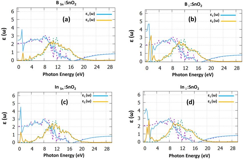
www.nature.com/scientificreports/
Regarding the electrical properties of the material, it was determined that B doping beneficially increases the
carrier concentration compared to the undoped S nO213.
Indium is an important dopant used to increase the electrical and optical properties of S nO214–16. Aouaj et al.14
compared the electrical and optical properties of ITO and FTO and they determined that at high In content the
absorbance is lower in ITO and the gap value is increased. Additionally, they predicted that that the electrical
resistivity is generally lower in ITO as compared to FTO. Finally, they concluded that ITO at different In con-
centration can be used as a transport layer or electrode in solar cells. Similar experiments of Kulkarni et al.15
showed that the deposition temperature and substrate play a major role regarding the optical properties of ITO
and variation to the refractive index value.
Apart from the experimental works, there are also theoretical studies based on DFT that examine the influence
of doping in S nO2, mostly in substitutional positions16–24. Especially for the halogen substitutional doping, it is
revealed that single donor states arise inside the bandgap; however, the effect of interstitials is not generally taken
into consideration by the community. Mallick et al.23 examined theoretically the impact of substitutional Al in
SnO2. They showed that the introduction of aluminium (Al) leads to new defect states above the Fermi energy
level which are highly depend on the doping concentration. The band gap of Al:SnO2 remains unchanged for low
doping concentrations (below 1.85%) while there is a small increase in high concentrations (higher than 3.70%).
Duan et al.24 investigated the effect of gallium (Ga) in S nO2 and determined that Ga substitutionals in Sn sites,
shifts the Fermi energy to the valence band and introduces more charge holes at the Ga sites. The Ga doping also
slightly reduces the band gap and increases the electrical conductivity of the material. Nevertheless, the effect of
B and In incorporation in S nO2 is not extensively examined using computational modelling techniques. From
all the above it is concluded that the B family group elements (group IIIA of the periodic table) introduce energy
states in the band gap which may play a major role in photovoltaic and photocatalytic devices.
In most previous DFT studies, the bandgap of SnO2 is considerably underestimated and predicted at a value
of 1–2 eV22,25. This is a well-known deficiency of the Local Density Approximation (LDA) and of the Generalized
Gradient Approximation (GGA). Therefore, the use of computationally demanding but more accurate hybrid
exchange–correlation functionals are deemed necessary to accurately describe the band gap and the position of
states in the gap or at its edges.
In the present study, we apply Hybrid functional DFT calculations using PBE045 to attain a bandgap value of
3.35 eV, which agrees well with the experimentally reported bandgap3,26. More analytically, we examine the effect
of B and In doping on the bulk SnO2 and we also investigate the effect of interstitial doping of the (110) surface
for the first time. Density of states (DOS) calculations showed a reduction of the band gap in all the substitu-
tional cases and the formation of energy states in the bandgap for the substitutional and interstitial doping. This
bandgap reduction combined with the created inter-gap energy levels are highly beneficial for the photocatalytic
applications of SnO2 while the predicted characteristics can also be applied in photovoltaic technologies.
Results
Bulk rutile SnO2. SnO2 forms in the P42/mmm space group crystalizing in the rutile structure. The exper-
imental unit cell parameters a = b = 4.737 Å and c = 3.186 Å were determined using X-ray diffraction (XRD)
experiments16. The calculated lattice parameters after the relaxation of rutile S nO2 are a = b = 4.717 Å and
c = 3.189 Å in very good agreement with the experimental values. The dopant percentage of the present calcula-
tions is 1 B or In atom in 48 S nO2 atoms, which results in 2.08% doping. Zhang et al.27 performed experiments
regarding the effect of B in tin oxide and they predicted that B can either be at a Sn substitutional site or occupy
an interstitial site. Zhang et al.27 determined that with this amount of doping the thickness of the film is reduced
in parallel with the mean crystal size. We predict that in its Sn substitutional site the B atom is at a distance of
1.775 Å from the nearest oxygen atom (refer to Fig. 1a) while for the interstitial case, the boron atom is at a
distance of 1.475 Å from the O-atom (refer to Fig. 1b). In Fig. 1c,d we show the InSn:SnO2 and I ni:SnO2 cases,
respectively. The substitutional dopant is relaxed at a distance of 2.11 Å from the nearest oxygen atom, while the
interstitial is located at a distance of 2.03 Å. In Fig. 1e we present the bulk supercell used. In Table 1, we report the
relevant lattice parameters and volume changes, through doping, for the bulk system. Concerning the B:SnO2
cases, there is a small decrease in the lattice volume for the substitutional case, which can be attributed to the
smaller ionic radius of B than Sn (B3+: 0.23 Å, Sn4+: 0.71 Å) while for the interstitial case, there is an increase.
The present results agree with the available experimental data that predict a decrease of the lattice parameters for
the BSn:SnO2 and an increase for the Bi:SnO29. Similarly for In:SnO2 we predicted that in all the cases, there is an
increase to the lattice parameters. This is in agreement with previous experimental s tudies28.
For each doping case, we calculate the DOS and the PDOS and present them in Fig. 2. The DOS of the
undoped SnO2 is given in Fig. 2e for reference. To have a clear and more reliable picture of the changes of the
electronic structure due to doping, we employed the hybrid functional PBE0, which provides a good bandgap
value (calculated at 3.35 eV) and is in agreement with the experimental v alue26.
In Fig. 2a, the BSn:SnO2 case is examined. In this case, it is observed from the total DOS (grey) that the
bandgap is reduced to the value of 2.73 eV while some energy states are created inside the bandgap at 1 eV. Fur-
thermore, it is seen that some additional states arise at the valence band maximum. Looking at the PDOS of the
B substitutional case, we predict that these states are created mostly from the hybridization of O-2p with Sn-5p
and the B-2p orbitals. This is in agreement with the work of Yu et al.29, which also predicts mid-gap states and
gap reduction when B is inserted. However, in their study, there is an underestimation to the bandgap value of
SnO2. Experimental studies30 have shown that 2% B doping decreases the bandgap, which is in good agreement
with the present study.
To further investigate the effect of B doping, we considered interstitial B in SnO2. We expect that the inter-
stitial incorporation of B results in gap states forming to the conduction band edge between 1.66 and 3.49 eV.
Scientific Reports | (2021) 11:13031 | https://doi.org/10.1038/s41598-021-92450-2 2
Vol:.(1234567890)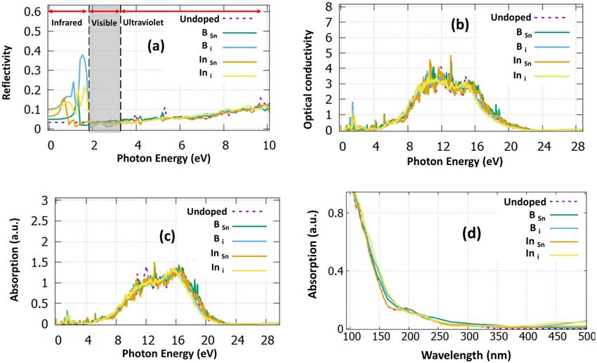
www.nature.com/scientificreports/
Figure 1. The structures of (a) boron substitutional doped SnO2 (BSn:SnO2), (b) boron interstitial doped SnO2
( Bi:SnO2), (c) indium substitutional doped SnO2 (InSn:SnO2), (d) indium interstitial doped SnO2 (Ini:SnO2) and
(e) the bulk supercell.
a (Å) c (Å) Vol (Å3)
SnO2 4.717 3.189 70.956
BSn:SnO2 4.674 3.153 68.881
Bi:SnO2 4.866 3.225 76.361
InSn:SnO2 4.730 3.194 71.459
Ini:SnO2 4.901 3.220 77.343
Table 1. The calculated lattice constants and cell volumes for all the dopants.
Scientific Reports | (2021) 11:13031 | https://doi.org/10.1038/s41598-021-92450-2 3
Vol.:(0123456789)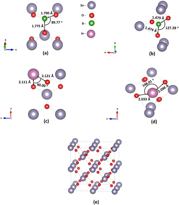
www.nature.com/scientificreports/
Figure 2. The total density of states (DOS) and the projected density of states (PDOS) of (a) BSn:SnO2, (b)
Bi:SnO2, (c) InSn:SnO2, (d) Ini:SnO2 and (e) undoped SnO2.
The bandgap is seen to increase to the value of 3.72 eV. As it is discussed in previous studies, the formation of
energy states in the middle of the bandgap is highly beneficial for photocatalytic applications, but still, they can
be a crucial disadvantage for PV and LED devices as they work as “traps” which reduce the device photocurrent
and the photogenerated charge carriers30,31. Although Bi:SnO2 has not been examined theoretically, Zhi et al.9
predicted that interstitial atomic positions play a significant role in increasing the capacity of tin oxide, making
it a good fit for supercapacitor applications. Zhi et al.9 used 4% B and they concluded that the interstitial atoms
slightly increased the bandgap. This is the Moss-Burstein effect and it is generally seen in heavily doped semi-
conductors, where after a doping concentration, the bandgap of the semiconductor starts to increase and can
even reach higher values than the undoped m aterial32. In the case of Bi:SnO2, this provides a sufficient number
of charge carriers that improve the capacitance of SnO233. We predicted a bandgap increase in the case of the
bulk SnO2 while in the (110) surface of S nO2 the gap remained unchanged. The (110) plane is considered the
most highly energetic plane of the experimental SnO2 structure9,34,35 as we discuss in the next section. In essence
the present calculations complete the DFT work of Zhi et al.9, which focused only to the (002) plane. Zhang
et al.27 also performed electrical measurements to predict the properties of B:SnO2. They predicted that in the
interstitial position, B releases three free electrons resulting in an increase of the free electron concentration.
Tran et al.13 predicted that the bandgap of SnO2 is decreased with the B incorporation and with the increase of
the temperature. While this is opposite to what we predicted or other experimental w orks9 we believe that this
is due to the effect of intrinsic defects, such as oxygen vacancies, which affect the gap value. Also, the percentage
of B atoms that reside in substitutional sites play an important role to the increase of the transmission of light
within SnO2. However, it is clear that even in this case the Moss-Burstein effect is still seen as the band gap is
increasing after the 4 at.% doping percentage.
Continuing with the bulk In:SnO2 we examined the interstitial and substitutional formation. Focusing on
the DOS of InSn:SnO2 (Fig. 2c) we predicted again unoccupied energy states near the valence band at 0.8 eV,
which are created due to the hybridization of O-2p with Sn-5p and In-5p. These gap states might be beneficial
Scientific Reports | (2021) 11:13031 | https://doi.org/10.1038/s41598-021-92450-2 4
Vol:.(1234567890)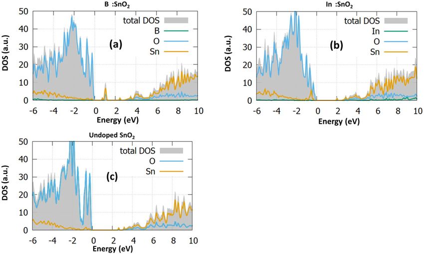
www.nature.com/scientificreports/
Figure 3. The dielectric function for (a) BSn:SnO2, (b) Bi:SnO2, (c) InSn:SnO2 and (d) Ini:SnO2. The dotted
purple and dotted green, correspond to the dielectric function of the undoped S nO2.
for device fabrication as they will serve as a route for the transition from the valence to the conduction band.
Furthermore, now the bandgap is slightly decreased at a value of 3.25 eV. Thereafter, we performed calcula-
tions for the interstitial doping of indium in SnO2. We predict that the In-5p orbitals play a significant role in
shifting the conduction band and reducing the band gap, which reaches a value of 3.48 eV. Similarly to the B
case, the interstitial doping gives rise to energy levels inside the gap in the area between 1.48 and 3.29 eV. The
present results agree well with the experimental data of Abdulsattar et al.36, which predicted a slight decrease to
the bandgap with a doping percentage of 2%. All these results show that although B:SnO2 shows energy states
that are detrimental for device applications, it is evident that gap reduction makes it possible for photocatalytic
applications. In contrast, In:SnO2 shows characteristics that make it a good candidate for an electron transport
layer material for photovoltaic devices.
To consider possible applications of the doped bulk structures, we calculated their optical properties. In
order to describe the absorption and dispersion mechanisms from the occupied to the empty electron levels,
we predicted the dielectric function, presented in Fig. 3. Focusing on the real part of the dielectric function for
the undoped S nO2 (dotted purple), it is seen that it reaches a maximum value of 8.5 eV. The negative value at
16.5 eV is attributed to the metallic properties of undoped SnO237,38. The imaginary part of the dielectric func-
tion provides helpful information regarding the probability of photon absorption. We calculated that there is a
decreasing trend for all the cases due to Maxwell–Wagner interfacial polarization39. From the undoped SnO2 case
(dotted green), two sharp peaks arise due to the transitions from O-2p to Sn-5p. The dielectric constant of the
undoped case is predicted at 2 in good agreement with previous e xperimental37 and theoretical w orks38. Focusing
on BSn:SnO2 (refer to Fig. 3a) case, we predicted the dielectric constant is significantly increased to the value of
2.5. The major peak that arises at 1.7 eV of the imaginary part can be attributed to the transition of electrons of
B-2p and Sn-5p. Continuing with the interstitial B case (refer to Fig. 3b), there is a considerable increase to the
dielectric constant, which reaches a value of 3.8.
Regarding the I nSn:SnO2 (Fig. 3c) the dielectric constant is increased to the value of 3, which is significantly
higher than the B Sn:SnO2 and finally, for the I ni:SnO2 (Fig. 3d) the dielectric constant reaches the value of 3.7.
From Fig. 3 it can also be observed that there is a shift of the low photon energy peaks towards the visible
region accompanied by an increase of the value of the dielectric constant. The recombination of charge carriers
decreases, where the static dielectric constant monitors the electric fields inside the material by polarization. As
a result, both B
i:SnO2 and I ni:SnO2 are highly preferred to use as heterojunction buffer layers in photovoltaic
applications.
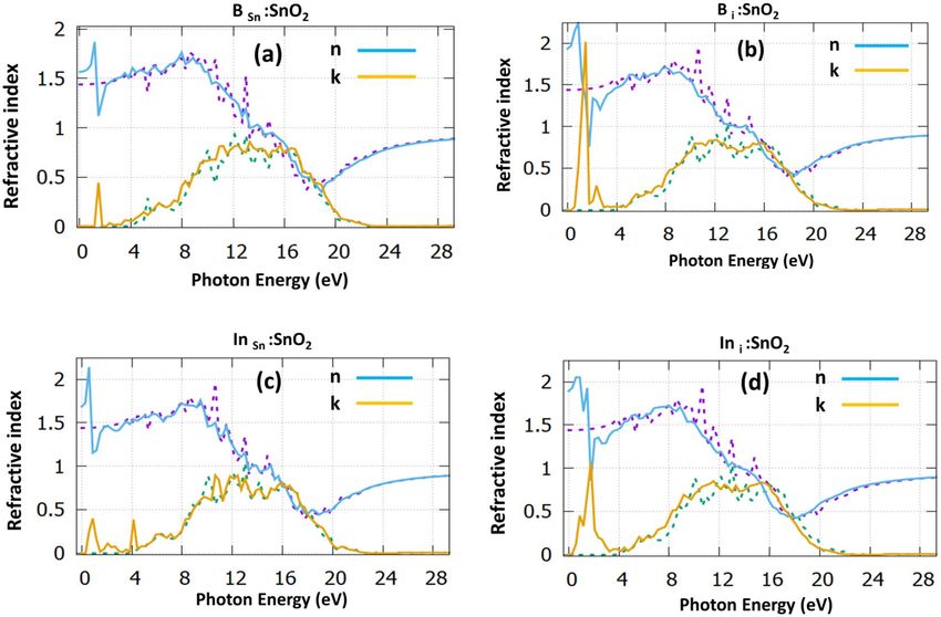
The refractive index is shown in Fig. 4. For the S nO2 the refractive index is computed in zero frequency at
the value of 1.40, which agrees with previous simulation s tudies38, but it is underestimated compared to the
experimental value of 1.7040.
Regarding the doping structures, we predicted a value of 1.55 for BSn:SnO2 (Fig. 4a), while for Bi:SnO2
(Fig. 4b), there is an increase reaching a value of 1.95. Considering In doping, we predicted a value of 1.6 for the
substitutional case (Fig. 4c) and a value of 1.85 for the interstitial In (Fig. 4d). It is evident that for the refractive
Scientific Reports | (2021) 11:13031 | https://doi.org/10.1038/s41598-021-92450-2 5
Vol.:(0123456789)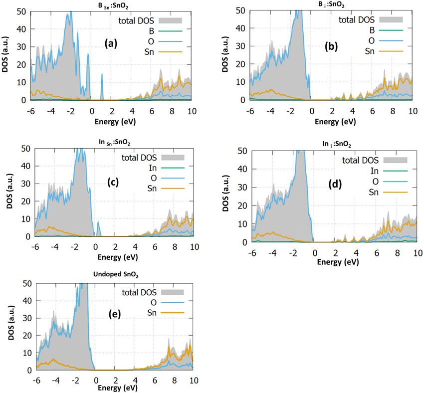
www.nature.com/scientificreports/
Figure 4. The refractive index for (a) BSn:SnO2, (b) Bi:SnO2, (c) InSn:SnO2 and (d) Ini:SnO2. The dotted purple
and dotted green, correspond to the dielectric function of the undoped S nO2.
Figure 5. (a) The reflectivity for all the doped structures (b) The optical conductivity for all the studied
structures (c) the absorption coefficient for all the structures versus the photon energy (d) the absorption
coefficient for all the structures versus the wavelength. The dotted purple and dotted green, correspond to the
undoped SnO2.
Scientific Reports | (2021) 11:13031 | https://doi.org/10.1038/s41598-021-92450-2 6
Vol:.(1234567890)
www.nature.com/scientificreports/
Bandgap (eV) Dielectric constant Refractive index Reflectivity
SnO2 3.33 2.0 1.40 0.03
BSn:SnO2 2.73 2.5 1.55 0.05
Bi:SnO2 3.72 3.8 1.95 0.1
InSn:SnO2 3.25 3 1.60 0.06
Ini:SnO2 3.48 3.7 1.85 0.095
Table 2. The calculated electronic and optical constants.
index, there is an increase in the lower photon energies and on the contrary, there is a significant decrease in the
upper energies. This is due to the optical dispersion that these structures have.
To provide a further insight into the optical properties of all these structures, in Fig. 5 we calculated the
reflectivity, the optical conductivity, and the absorption of the structures. Reflectivity (see Fig. 5a) is an important
property of these materials as it signifies the amount of photons that are reflected from the material. We have
shown that the values at zero photon energy are calculated at 3%, 5%, 10%, 6% and 9.5% for S nO2, BSn:SnO2,
Bi:SnO2, InSn:SnO2 and Ini:SnO2 respectively. We predicted that B i:SnO2 has the highest reflectivity in the near-
infrared and visible regions compared to all the other cases. Importantly, all the examined cases encounter less
than 15% reflectivity in the infrared and visible region; thus they can be used as antireflective coatings when the
dopant concentration is at 2%41. In Table 2 we have gathered all the calculated electrical and optical constants
for reference.
In Fig. 5b we present the optical conductivity of all the calculated structures. If a photon has higher energy
than the optical bandgap then a transition occurs and an electron–hole pair (exciton) is generated. The mobil-
ity of these excitons represent the optical conductivity, which is an important parameter that is used to design
optical detectors42. Due to the electronic charge neutrality, these excitons do not contribute to the electrical
conductivity43. The highest excitonic features are calculated at 13.2 eV for undoped, BSn:SnO2 and InSn:SnO2 cases
while for the interstitial dopants they are shifted to 9 eV and 10 eV for the B and In, respectively. The optical con-
ductivity also describes the losses for a wave with the same frequency. From the graph, we can conclude that S nO2
and Ini:SnO2 have lower losses than the other cases. Lastly, in Fig. 5c,d we present the absorption co-efficiency.
The absorption for the undoped case starts at 380 nm, which is underestimated compared to the experimental
value, which is approximately 400 nm44. It is seen that Ini and Bi have the highest absorption to the visible region.
From the above, we can conclude that B i and I ni doped S nO2 exhibits interesting characteristics, constituting
the material applicable to photovoltaic and photocatalytic devices.
Surface (110) of rutile SnO2. As Zhi et al.9 indicated to further understand the effect of Bi, the surface of
S nO2 needs to be examined. For applicable photocatalytic materials with a visible light response and high charge
mobility, such as SnO2, attention to the high-energy surfaces should be paid when the structure is doped with
atoms or molecules. The studies of SnO2 surface are significantly less than the studies of the bulk and they pri-
marily focus on sensor a pplications45. In this section, the change to the electronic properties of B and In doped
SnO2 will be investigated. Here we used a slab model with a vacuum of 12 Å thickness across the (110) plane.
We chose this particular surface because it is the most intense crystallization p lane9,45 of rutile S nO2 and it has
never been studied before for B or In doping. Furthermore, as the (110) plane is one of the most highly energetic
surfaces, it will play the role of the active site in photocatalytic reactions46. Indium doping improves the electri-
cal characteristics in S nO2 nanowire structures. Specifically, the field enhancement factor is higher compared to
other dopants47–49. In these applications, the surface of the nanowire plays a significant role and it is responsible
for the fluctuations in the field emission properties47.
Here we predicted the interstitial position of both B and In by examining many different configurations
and keeping the lowest energy system. To accurate predict the electronic characteristics, we used the hybrid
functional PBE0.
In Fig. 6a,b we present the B i:SnO2 and In i:SnO2 doping cases while in Fig. 6c the supercell for the (110) plane
is presented for reference. The boron interstitial displaces the tin atom and occupies a tin site to minimize its
energy (Fig. 6a). We predicted that interstitial boron sites at 2.182 Å from the nearest oxygen atom and 3.10 Å
from the nearest tin atom. On the other hand, we calculated that In atom sites at a distance of 2.183 Å from the
nearest oxygen atom and 3.32 Å from the nearest tin atom. Looking at the DOS and the pDOS of Fig. 7a, it is
seen that boron interstitial produces a small band peak at 1 eV.
Interestingly in this high-energy plane the bandgap is not decreased compared to the undoped case (see
Fig. 7c). We believe that this result combined with the bulk B i:SnO2 explains the experimental phenomenon that
Zhi et al.9 discussed in their paper about B i. Looking at the I ni:SnO2 (refer to Fig. 7b) we can see that the (110)
surface bandgap decreases to 2 eV. Indium doping of the surface S nO2 improves the sensitivity of tin oxide based
gas sensors as it significantly affects the crystallization of the s amples50. The gap of the undoped (110) S nO2 is
shown in Fig. 7c at 2.5 eV, a good agreement with previous DFT studies51. All the above results indicate that In
doping in the SnO2 shows good characteristics that should be examined in photocatalytic applications.
Scientific Reports | (2021) 11:13031 | https://doi.org/10.1038/s41598-021-92450-2 7
Vol.:(0123456789)www.nature.com/scientificreports/
Figure 6. The structures of (a) boron doped (110) SnO2 surface, (b) indium doped (110) SnO2 surface and (c)
the (110) surface supercell.
Figure 7. The total density of states (DOS) and the projected density of states (PDOS) of (a) B (b) In and (c)
undoped (110) SnO2 surface.
Scientific Reports | (2021) 11:13031 | https://doi.org/10.1038/s41598-021-92450-2 8
Vol:.(1234567890)www.nature.com/scientificreports/
Conclusions
In the present study, we applied DFT calculations to investigate the electronic and optical properties of boron and
indium doped bulk and surface S nO2. In particular, we performed DOS calculations and we found that the bulk
structures have a bandgap increase for interstitial boron and indium doping. Conversely, for the substitutional
cases, the bandgap is notable decreased. Mid-gap states are formed in all the examined cases. Although these
states might be detrimental for photovoltaics as they may act as trap states for photogenerated carriers, they can
be useful for photocatalytic applications based on B:SnO2 and In:SnO2. The present study explains some of the
phenomena that have been experimentally observed and paves the way for applications of boron and indium
structures to more applications such as supercapacitors or sensors. Regarding the indium defect, we predicted
that at low concentrations highly wanted states are formed near the valence band, which can be beneficial for
energy harvesting devices. Furthermore, its optical characteristics and the bandgap reduction at the surface make
it a worthy candidate for photocatalysis.
Methodology
We employed the Cambridge Serial Total Energy Package (CASTEP)52,53. For our calculations we used the hybrid
functional PBE0 in order to consider the effect of the localized electrons and the bandgap underestimation
that is generally encountered in GGA and L DA54. The cutoff energy was chosen at 800 eV after performing the
convergence test and for our calculations we used a 48 atom supercell (2 × 2 × 2 unit cells) with 2 × 2 × 3 k-points
for the sampling of the Brillouin zone during the geometry o ptimization54. To predict the interstitial positions
in all cases, we used geometry optimization and we examined all possible configurations. Finally, we kept the
position, which provides the lowest energy system. For the simulation of the surface we used a slab model with a
vacuum of approximately 12 Å vertical to the (110) direction. In our system, the top 2 layers represent the surface
while the bottom 2 are fixed and mimic the bulk region. For the DOS calculations we used a k-point mesh of
5 × 5 × 5 for the bulk modelling while for the surface we applied a 3 × 3 × 1 set. Finally, the convergence criteria
for our simulations were chosen at 2.0 ∙ 1 0−5 eV/atom for the SCF tolerance, 0.05 eV/Å for the force tolerance
and 0.001 Å for the Max displacement tolerance.
Received: 4 April 2021; Accepted: 3 June 2021
References
1. Searle, A. B. The Glazer’s Book (The Technical Press, 1935).
2. Holleman, A. F. & Wiberg, E. Inorganic Chemistry (Academic Press, 2001).
3. Greenwood, N. N. & Earnshaw, A. Chemistry of the Elements (Elsevier, 2012).
4. Tountas, M. et al. Water-soluble lacunary polyoxometalates with excellent electron mobilities and hole blocking capabilities for
high efficiency fluorescent and phosphorescent organic light emitting diodes. Adv. Funct. Mater. 26(16), 2655–2665 (2016).
5. Wang, C. et al. Ultrathin S nO2 nanosheets: Oriented attachment mechanism, nonstoichiometric defects, and enhanced lithium-ion
battery performances. J. Phys. Chem. C 116(6), 4000–4011 (2012).
6. Rakhshani, A. E., Makdisi, Y. & Ramazaniyan, H. A. Electronic and optical properties of fluorine-doped tin oxide films. J. Appl.
Phys. 83(2), 1049–1057 (1998).
7. Filippatos, P. P., Kelaidis, N., Vasilopoulou, M., Davazoglou, D. & Chroneos, A. Defect processes in halogen doped S nO2. Appl.
Sci. 11(2), 551 (2021).
8. Minami, T. Transparent conducting oxide semiconductors for transparent electrodes. Semicond. Sci. Technol. 20, S35–S44 (2005).
9. Zhi, J., Zhou, M., Zhang, Z., Reiser, O. & Huang, F. Interstitial boron-doped mesoporous semiconductor oxides for ultratransparent
energy storage. Nat. Commun. 12(1), 1–12 (2021).
10. Kong, X. B., Li, F., Qi, Z. N., Qi, L. & Yao, M. M. Boron-doped tin dioxide films for environmental applications. Surf. Rev. Lett.
24(05), 1750059 (2017).
11. Zhao, W., Ma, W. H., Chen, C. C., Zhao, J. C. & Shuai, Z. G. Efficient degradation of toxic organic pollutants with Ni2O3/TiO2−xBx
under visible irradiation. J. Am. Chem. Soc. 126, 4782 (2004).
12. Bagwasi, S., Tian, B., Zhang, J. & Nasir, M. Synthesis, characterization and application of bismuth and boron co-doped T iO2: A
visible light active photocatalyst. Chem. Eng. J. 217, 108 (2013).
13. Tran, Q. P., Fang, J. S. & Chin, T. S. Optical properties and boron doping-induced conduction-type change in S nO2 thin films. J.
Electron. Mater 45(1), 349–356 (2016).
14. Aouaj, M. A., Diaz, R., Belayachi, A., Rueda, F. & Lefdil, M. A. Comparative study of ITO and FTO thin films grown by spray
pyrolysis. Mater. Res. Bull. 44, 1458 (2009).
15. Kulkarni, A. K., Lim, T., Khan, M. & Schulz, K. H. Electrical, optical, and structural properties of indium-tin-oxide thin films
deposited on polyethylene terephthalate substrates by RF sputtering. J. Vac. Sci. Technol. A 16, 1636 (1998).
16. Peng-Fei, L. et al. Electronic structure and optical properties of antimony-doped SnO2 from first-principle study. Commun. Theor.
Phys. 57, 145 (2012).
17. Canestraro, C. D., Roman, L. S. & Persson, C. Polarization dependence of the optical response in SnO2 and the effects from heavily
F doping. Thin Solid Films 517(23), 6301–6304 (2009).
18. Rivera, R., Marcillo, F., Chamba, W., Puchaicela, P. & Stashans, A. S nO2 physical and chemical properties due to the impurity
doping. Lect. Notes Eng. Comp. 2, 814–818 (2013).
19. Velikokhatnyi, O. I. & Kumta, P. N. Ab-initio study of fluorine-doped tin dioxide: A prospective catalyst support for water elec-
trolysis. Phys. B 406(3), 471–477 (2011).
20. Golovanov, V., Golovanova, V., Kuisma, M. & Rantala, T. T. Electron spin resonance parameters of cation vacancies in tin dioxide
doped with fluorine and hydrogen. J. Appl. Phys. 114(14), 143907 (2013).
21. Oshima, M. & Yoshino, K. Structural and electronic structure of S nO2 by the first-principle study. Trans Tech Stäfa 725, 265–268
(2012).
22. Govaerts, K., Partoens, B. & Lamoen, D. Extended homologous series of Sn–O layered systems: A first-principles study. Solid State
Commun. 243, 36–43 (2016).
23. Mallick, H. K., Zhang, Y., Pradhan, J., Sahoo, M. P. K. & Pattanaik, A. K. Influence of particle size and defects on the optical,
magnetic and electronic properties of Al doped S nO2 nanoparticles. J. Alloys Compd. 854, 156067 (2021).
Scientific Reports | (2021) 11:13031 | https://doi.org/10.1038/s41598-021-92450-2 9
Vol.:(0123456789)www.nature.com/scientificreports/
24. Duan, Y. et al. Effects of Ga doping and hollow structure on the band-structures and photovoltaic properties of SnO2 photoanode
dye-sensitized solar cells. RSC Adv. 5(114), 93765–93772 (2015).
25. Perdew, J. P. & Levy, M. Physical content of the exact Kohn–Sham orbital energies: Band gaps and derivative discontinuities. Phys.
Rev. Lett. 51(20), 1884 (1983).
26. Zervos, M. et al. Epitaxial highly ordered Sb:SnO2 nanowires grown by the vapor liquid solid mechanism on m-, r- and a-Al2O3.
Nanoscale Adv. 1, 1980–1990 (2019).
27. Zhang, B., Tian, Y., Zhang, J. X. & Cai, W. The structural and electrical studies on the Boron-doped SnO2 films deposited by spray
pyrolysis. Vacuum 85(11), 986–989 (2011).
28. Lekshmy, S. S. & Joy, K. Structural and optoelectronic properties of indium doped SnO2 thin films deposited by sol gel technique.
J. Mater. Sci. Mater. Electron. 25(4), 1664–1672 (2014).
29. Yu, J. et al. Structural and electronic properties of SnO2 doped with non-metal elements. J Nanotechnol. 11(1), 1321–1328 (2020).
30. Filippatos, P. P. et al. Defect processes in F and Cl doped anatase T iO2. Sci. Rep. 9, 19970 (2019).
31. Filippatos, P. P. et al. Preparation of hydrogen, fluorine and chlorine doped and co-doped titanium dioxide photocatalysts: A
theoretical and experimental approach. Sci. Rep. 11, 5700 (2021).
32. Butcher, K., Hirshy, H., Perks, R. M., Wintrebert, M. & Chen, P. P. T. Stoichiometry effects and the Moss-Burstein effect for InN.
Phys. Status Solidi A 203, 66–74 (2006).
33. Simon, P. & Gogotsi, Y. Materials for electrochemical capacitors. Nat. Mater. 7, 845–854 (2008).
34. Kumar, M., Kumar, A. & Abhyankar, A. C. S nO2 based sensors with improved sensitivity and response-recovery time. Ceram. Int
40(6), 8411–8418 (2014).
35. Manassidis, I., Goniakowski, J., Kantorovich, L. N. & Gillan, M. J. The structure of the stoichiometric and reduced SnO2 (110)
surface. Surf. Sci. 339(3), 258–271 (1995).
36. Abdulsattar, M. A., Batros, S. S. & Addie, A. J. Indium doped SnO2 nanostructures preparation and properties supported by DFT
study. Superlattices Microstruct. 100, 342–349 (2016).
37. Tingting, S., Fuchun, Z. & Weihu, Z. Density functional theory study on the electronic structure and optical properties of S nO2.
Rare Metal Mater. Eng. 44(10), 2409–2414 (2015).
38. Khan, A. F., Mehmood, M., Aslam, M. & Ashraf, M. Characteristics of electron beam evaporated nanocrystalline S nO2 thin films
annealed in air. Appl. Surf. Sci. 256(7), 2252–2258 (2010).
39. Singh, A., Chatterjee, R., Mishra, S. K., Krishna, P. S. R. & Chaplot, S. L. Origin of large dielectric constant in La modified BiFeO3–
PbTiO3 multiferroic. J. Appl. Phys. 111(1), 014113 (2012).
40. Afify, H. H., Momtaz, R. S., Badawy, W. A. & Nasser, S. A. Some physical properties of fluorine-doped S nO2 films prepared by
spray pyrolysis. J. Mater. Sci. Mater. Electron. 2(1), 40–45 (1991).
41. Khoshman, J. M. & Kordesch, M. E. Optical properties of a-HfO2 thin films. Surf. Coat. Technol. 201(6), 3530–3535 (2006).
42. Akinlami, J. O. & Olateju, I. O. Reflection coefficient and optical conductivity of gallium nitride GaN. Quant. Electron. Optoelectron.
15(3), 281–284 (2012).
43. Dash, L. K., Vast, N., Baranek, P., Reining, M. C. & Cheynet, L. Electronic structure and electron energy-loss spectroscopy of Z rO2
zirconia. Phys. Rev. B 70(24), 245116 (2004).
44. Doyan, A., Susilawati, & Imawanti, Y. D. Synthesis and characterization of SnO2 THIN layer with a doping aluminum is deposited
on quartz substrates. AIP AIP Conf. Proc. 1801(1), 020005 (2017).
45. Wang, X., Qin, H., Chen, Y. & Hu, J. Sensing mechanism of S nO2 (110) surface to CO: Density functional theory calculations. J.
Chem. Phys. C 118(49), 28548–28561 (2014).
46. Talebian, N. & Jafarinezhad, F. Morphology-controlled synthesis of SnO2 nanostructures using hydrothermal method and their
photocatalytic applications. Ceram. Int. 39(7), 8311–8317 (2013).
47. Bhise, A. B. et al. A single In-doped SnO2 submicrometre sized wire as a field emitter. J. Phys. D: Appl. Phys. 40, 3644–3648 (2007).
48. Bhise, A. B. et al. Sb-doped S nO2 wire: Highly stable field emitter. J. Cryst. Growth 307, 87–91 (2007).
49. Bhise, A. B. et al. Field emission investigations of R uO2-doped SnO2 wires. Appl. Surf. Sci. 253, 9159–9163 (2007).
50. Cui, S. et al. Indium-doped S nO2 nanoparticle–graphene nanohybrids: Simple one-pot synthesis and their selective detection of
NO2. J. Mater. Chem. A 1(14), 4462–4467 (2013).
51. Li, M., Zhu, H., Wei, G., He, A. & Liu, Y. DFT calculation and analysis of the gas sensing mechanism of methoxy propanol on Ag
decorated SnO2 (110) surface. RSC Adv. 9(61), 35862–35871 (2019).
52. Segall, M. D. et al. First-principles simulation: Ideas, illustrations and the CASTEP code. J. Phys. Cond. Matter 14(11), 2717–2744
(2002).
53. Ceperley, D. M. & Alder, B. J. Exchange-correlation potential and energy for density-functional calculation. Phys. Rev. Lett. 45,
567–581 (1980).
54. Paier, J. et al. Screened hybrid density functionals applied to solids. J. Chem. Phys. 124, 154709 (2006).
Acknowledgements
P.P.F., M.V., D.D. and A.C. are grateful for LRF ICON funding from the Lloyd’s Register Foundation, a charitable
foundation helping to protect life and property by supporting engineering-related education, public engagement
and the application of research. N.K. acknowledges support from European Union’s H2020 Programme under
Grant Agreement No 824072-HARVESTORE.
Author contributions
P.P.F. and N.K. performed the calculations. P.P.F., N.K., M.V., D.D. and A.C. contributed to the interpretation of
the results and the writing of the paper.
Competing interests
The authors declare no competing interests.
Additional information
Correspondence and requests for materials should be addressed to A.C.
Reprints and permissions information is available at www.nature.com/reprints.
Publisher’s note Springer Nature remains neutral with regard to jurisdictional claims in published maps and
institutional affiliations.
Scientific Reports | (2021) 11:13031 | https://doi.org/10.1038/s41598-021-92450-2 10
Vol:.(1234567890)www.nature.com/scientificreports/
Open Access This article is licensed under a Creative Commons Attribution 4.0 International
License, which permits use, sharing, adaptation, distribution and reproduction in any medium or
format, as long as you give appropriate credit to the original author(s) and the source, provide a link to the
Creative Commons licence, and indicate if changes were made. The images or other third party material in this
article are included in the article’s Creative Commons licence, unless indicated otherwise in a credit line to the
material. If material is not included in the article’s Creative Commons licence and your intended use is not
permitted by statutory regulation or exceeds the permitted use, you will need to obtain permission directly from
the copyright holder. To view a copy of this licence, visit http://creativecommons.org/licenses/by/4.0/.
© The Author(s) 2021
Scientific Reports | (2021) 11:13031 | https://doi.org/10.1038/s41598-021-92450-2 11
Vol.:(0123456789)You can also read