2-ΜM SINGLE LONGITUDINAL MODE GASB-BASED LATERALLY COUPLED DISTRIBUTED FEEDBACK LASER WITH REGROWTH-FREE SHALLOW-ETCHED GRATINGS BY INTERFERENCE ...
←
→
Page content transcription
If your browser does not render page correctly, please read the page content below
Chin. Phys. B Vol. 25, No. 2 (2016) 024204

            2-µm single longitudinal mode GaSb-based laterally coupled
            distributed feedback laser with regrowth-free shallow-etched
                        gratings by interference lithography∗
                           Cheng-Ao Yang(杨成奥)1,2 , Yu Zhang(张宇)1,2 , Yong-Ping Liao(廖永平)1,2 ,
                         Jun-Liang Xing(邢军亮)1,2 , Si-Hang Wei(魏思航)1,2 , Li-Chun Zhang(张立春)1,2 ,
                       Ying-Qiang Xu(徐应强)1,2 , Hai-Qiao Ni(倪海桥)1,2 , and Zhi-Chuan Niu(牛智川)1,2,†
       1 State Key Laboratory for Superlattices and Microstructures, Institute of Semiconductors, Chinese Academy of Sciences, Beijing 100083, China
     2 Synergetic Innovation Center of Quantum Information and Quantum Physics, University of Science and Technology of China, Hefei 230026, China

                        (Received 5 July 2015; revised manuscript received 10 September 2015; published online 20 December 2015)

                  We report a type-I GaSb-based laterally coupled distributed-feedback (LC-DFB) laser with shallow-etched gratings
            operating a continuous wave at room temperature without re-growth process. Second-order Bragg gratings are fabricated
            alongside the ridge waveguide by interference lithography. Index-coupled LC-DFB laser with a cavity of 1500 µm achieves
            single longitudinal mode continuous-wave operation at 20 ◦ C with side mode suppression ratio (SMSR) as high as 24 dB.
            The maximum single mode continuous-wave output power is about 10 mW at room temperature (uncoated facet). A low
            threshold current density of 230 A/cm2 is achieved with differential quantum efficiency estimated to be 93 mW/A. The
            laser shows a good wavelength stability against drive current and working temperature.

            Keywords: laterally coupled distributed feedback laser, LC-DFB, interference lithography, GaSb, second-
                      order Bragg grating
            PACS: 42.55.Px, 78.55.Cr, 78.67.De, 42.60.Pk                       DOI: 10.1088/1674-1056/25/2/024204

1. Introduction                                                                ricated on the wafer, after that, an epitaxial re-growth step is
      The semiconductor laser diode based on Al-                               necessary to complete the growth of the laser epitaxy. [12,13]
GaAsSb/InGaAsSb alloys grown on GaSb substrates is at-                         Although the re-growth technique is common and mature in
tracting more and more attention in mid-infrared applications                  InP-based DFB lasers, it is particularly difficult in the case
such as remote gas sensing, [1] molecular spectroscopy, [2] med-               of GaSb-based laser due to the oxidation of the high Al con-
ical and defense applications [3] for its small size and excellent             tent in the epitaxy. [14] Miller et al. proposed a regrowth-free
laser property. Many industrial and harmful gaseous byprod-                    DFB structure in which the gratings were located alongside
ucts such as CO, HF, CO2 and H2 O have strong absorption                       the ridge-waveguide. The laser structure was completed in a
features in the wavelength range between 1.9 µm and 5 µm                       single epitaxy layer growth step and avoided the difficulty in
which is fully covered by GaSb-based laser diode. [4–6] For de-                the re-growth process. This kind of laser was later named ‘lat-
signing a lidar system for gas sensing, a tunable diode laser ab-              erally coupled’ DFB (LC-DFB) laser. [15] LC-DFB is aimed
sorption spectroscopy (TD-LAS) laser with narrow linewidth                     at avoiding the oxidation of Al content in the epitaxy after
is particularly important, which has been reported in previous                 the defining of grating, and it can also be used in GaAs and
literature. [1,7,8] GaSb-based Fabry–Perot (FP) laser exhibits                 InP material to avert the re-growth step. [15–17] The GaAs- and
mode hops and is inapplicable for this kind of application. [9]                InP-based LC-DFB lasers showed a good laser property which
Lasers with a mode selecting function such as distributed feed-                was very competitive compared with the traditional DFB laser
back lasers show excellent characteristics in narrow linewidth                 and attracted a lot of attention. [15–17] So far, the continuous
and single longitudinal mode emission, thus they are the ideal                 wave operation of GaSb-based LC-DFB laser diodes were re-
candidates for gas sensing applications. [10,11]                               ported to emit light beams at wavelengths of 2 µm, 2.3 µm,
      The conventional fabrication of InP-based DFB lasers                     2.6 µm, 2.8 µm, 3.4 µm. [5,18–20] Owing to the mode selecting
emitting around 2 µm requires two to three high-quality epi-                   mechanism of LC-DFB lasers, the defining of subsize grating
taxial growths, the first epitaxial process stops after the growth             is the most important and difficult part. Among the reports
of the waveguide layer, then a Bragg grating structure is fab-                 of LC-DFB lasers, Bragg grating has been fabricated using e-
∗ Projectsupported by the National Key Basic Research Program of China (Grant Nos. 2014CB643903 and 2013CB932904), the National Special Funds for
 the Development of Major Research Equipment and Instruments, China (Grant No. 2012YQ140005), the National Natural Science Foundation of China
 (Grant Nos. 61435012, 61274013, 61306088, and 61290303), and the Strategic Priority Research Program (B) of the Chinese Academy of Sciences (Grant
 No. XDB01010200).
† Corresponding author. E-mail: zcniu@semi.ac.cn

© 2016 Chinese Physical Society and IOP Publishing Ltd                                           http://iopscience.iop.org/cpb http://cpb.iphy.ac.cn

                                                                       024204-1
Chin. Phys. B Vol. 25, No. 2 (2016) 024204
beam lithography (EBL), [15,16,21] nanoimprint lithography, [22] waveguide is carefully etched to an inclination of 60◦ with re-
and interference lithography. [23] EBL is good at assuring the spect to the horizontal direction, which is an experienced in-
grating quality but it is expensive and fabrication-inefficient, clination at which the grating quality and laser property reach
which is costly and time consuming. [7] Interference lithogra- their equilibrium points after a large number of experiments.
phy and nanoimprint lithography are good at defining Bragg Figure 2 shows the scanning electron micrograph (SEM) of the
grating on a planar epitaxy surface but they present a big prob- slant ridge waveguide. Owing to the principle of interference
lem in transferring the surface grating deep into the waveguide lithography, the top of the ridge waveguide is also patterned
layer as a high aspect ratio is needed in dry etching. To be with a second-order-grating photoresist mask which will be
specific, the traditional fabrication schedule is first patterning transferred into the ridge waveguide in the grating etching pro-
grating on the top of the epitaxy, followed by the defining of cess. The formation of the grating on the ridge waveguide will
the ridge waveguide with photolithography. To form a good cause the problem of a contact window opening as a dielectric
coupling coefficient, the ridge waveguide and grating are then layer will be deposited after the etching of the grating to form
etched deep to the waveguide layer in one etching process, index-coupled mechanism and insulation. The grating on the
which brings problems to the deep dry etching as a high as- top of the ridge waveguide is also filled with dielectric. Thus
pect ratio (normally 20:1) is required to transfer the surface
the contact window opening is particularly difficult due to the
grating deep into the waveguide layer. [23]
different selection ratios between dielectric and GaSb mate-
rial in dry etching which will do harm to the obtainment of
2. Device design and fabrication p-side Ohm contact and reduce the laser property eventually.
To solve the aforementioned problems and reduce the as- To protect the ridge waveguide in the grating etching process
pect ratio in dry etching, we report an improved new approach and form shallow etching grating adjacent to the ridge waveg-
to fabricating an index coupled LC-DFB laser with second- uide, a SiNx protecting mask needs to be deposited before the
order grating by interference lithography. Figure 1 shows defining of the ridge waveguide. During the etching of the
the schematic diagram of our LC-DFB laser structure. This grating, the top SiNx layer has a larger section ratio than the
approach enables the fabricating of single-longitudinal-mode AlGaAsSb, thus if the SiNx layer is thick enough, the top GaSb
lasers following a single epitaxial growth process and the de- contact layer can be totally protected after the shallow grating
creasing of the aspect ratio in grating etching. Unlike the tra- etching. To the best of our knowledge this is the first GaSb-
ditional defining process of gratings by interference lithogra- based LC-DFB laser with interference-lithography-patterned
phy mentioned above, [23] we divide the fabrication of ridge grating on a non-planar surface. The improved process not
waveguide and grating into two steps; the ridge waveguide is only avoids the re-growth of high Al content epitaxy but also
first defined and etched by dry etching and the grating is then reduces the high aspect ratio in grating defining. The laser
formed alongside the ridge waveguide and etched to a shallow fabricated by our process emits up to 10-mW light beams in a
depth. The shallow etching of the grating sharply reduces the single longitudinal mode operation at room temperature with
an SMSR in excess of 24 dB without facet coating.
high aspect ratio in dry etching demanded by the traditional
deep etching approach, but shows little loss in the coupling
coefficient as it is also etched close to the waveguide com-
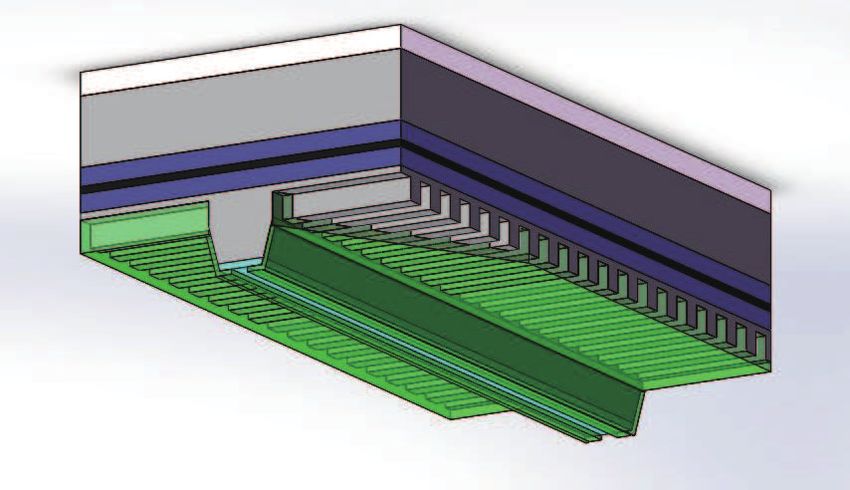
GaSb contact layer SiNx
pared with the conventional deep etching fabrication, which
eventually causes little difference in the laser property. What P cladding layer
is more, we have chosen the second-order Bragg grating which QW
further enlarges the etching width and reduces the aspect ratio.
As the ridge waveguide is first defined and etched, the epitaxy
ready for interference lithography is patterned and has a height
difference which will cause problems of photoresist stacking
aside the sidewall during interference lithography and eventu- N cladding layer
ally make the formation of grating adjacent to the ridge much GaSb substrate
more difficult. Owing to the coupling principle of LC-DFB,
gratings near the ridge are the most important part and have Fig. 1. (color online) Schematic diagram of our index-coupled LC-DFB
a great influence on laser performance. In order to solve the laser structure.
problem of nonuniform photoresist coating and form a high- The GaSb-based laser structure is grown on an n-
quality grating patterned by interference lithography, the ridge type GaSb (100) substrate by using solid–source molec-
024204-2Chin. Phys. B Vol. 25, No. 2 (2016) 024204
ular beam epitaxy (MBE). The epilayer structure con-
tains an n-doped Gasb buffer layer followed by a 1.5-µm
n-doped Al0.9 Ga0.1 As0.02 Sb0.98 cladding layer. The un-
ridge
doped active layer consists of 20 nm/10 nm three pairs waveguide
of In0.2 Ga0.8 Sb/Al0.4 Ga0.6 As0.02 Sb0.98 quantum wells (QWs)
(a)
with a compressive strain of 1.0% located in the central
part of an undoped 400-nm Al0.4 Ga0.6 As0.02 Sb0.98 waveg-
uide layer. [4] The upper cladding layer is composed of p- grating
doped Al0.9 Ga0.1 As0.02 Sb0.98 layer with a thickness of 1.5 µm
followed by a 250-nm highly doped GaSb contact layer for
achieving a good Ohm contact with the p-side electrode men-
tal.
1 mm
Ο ridge waveguide (b)
61.4 P cladding layer
QWs
grating
N cladding layer
1 mm
GaSb buffer
250 nm
Fig. 2. Scanning electron micrograph of the slant ridge waveguide.
The design of our LC-DFB lasers is based on the effec-
tive coupling coefficient, the modal effective refractive index Fig. 3. (color online) SEM picture of LC-DFB laser with second-order
grating fabricated by interference lithography. (a) Top view of the laser
of the unperturbed ridge laser is numerically calculated by us- after the deposition of p-side metal (Ti/Pt/Au), (b) sectional view of
ing a full-vector finite-difference calculation. [21] Assuming an grating after dry etching.
effective-medium index for the grating region, the neff is calcu- Figure 3 shows a scanning electron micrograph of an LC-
lated to be 3.45 while the electric-field overlap factor Γgrating , DFB laser. A 200-nm SiNx layer is first deposited on the top
which describes the extent to which the electric field overlaps of the epitaxy using plasma enhanced chemical vapor deposi-
with the grating is calculated to be 0.46%, thus the second- tion (PECVD) as etching protecting layer during the shallow
order grating width is calculated to be 580 nm for a wave range etching of gratings. The ridge waveguide is then patterned us-
of 2 µm. Using the approximation employed in Ref. [24], the ing contact lithography. The SiNx protecting layer and epitaxy
feedback effect of the lateral gratings can be quantified by es- is etched to a total depth of 1.4 µm using an inductively cou-
timating the grating coupling coefficient, pled plasma (ICP) with CHF3 and a gas mixture of Ar2 and
Cl2 respectively. The sample is then spin-coated with photore-
n2clad − n2cover sin(mπg/Λ )
κ= Γgrating , sist and the second-order grating is defined alongside the ridge
neff λ m
waveguide by interference lithography, due to the thin film of
where nclad is the index of the upper cladding layer into which photoresist used in interference lithography, another 100-nm
the grating is etched, ncover is the index of the SiNx dielectric SiNx transferring layer is deposited on the epitaxy before in-
filling the grating, g is the width of the grating teeth measured terference lithography to transfer a high quality mask for grat-
to be 240 nm, m is the relevant grating diffraction order, and ing etching. The Bragg grating is first transferred to the SiNx
Λ is the grating pitch. For a cavity length L = 1.5 mm, the κL transferring layer by reactive-ion etching (RIE), then the grat-
is estimated to be 1.1, a typical κL value to optimize modal ing is etched to a depth of 400 nm using the SiNx transferring
discrimination and optical power. [25] layer as mask by ICP. The ridge waveguide is completely pro-
024204-3Chin. Phys. B Vol. 25, No. 2 (2016) 024204
tected in the ICP process as the 200-nm thick SiNx protecting gain spectrum and the grating wavelength.
layer on the top of the ridge waveguide remains 100-nm thick
after transferring the grating to the SiNx transferring layer, 1.6 10
the resulting 100-nm SiNx layer is thick enough to protect the
8
ridge during the grating etching. The shallow etched grating is 1.2
Voltage/V
Power/mW
150 nm above the active range to form a good coupling with 6
the light. Thus we achieve a high quality grating alongside 0.8
4
the ridge waveguide to form a good coupling with the light.
0.4 2
Another SiNx layer is deposited on the samples with PECVD
after the etching of the grating for insulation and planariza-
0 0
tion. Finally, an ICP dry etching is used to open a contact 0 100 200 300 400 500
window in the SiNx . The p-side top Ohm contacts are formed Current/mA
by Ti/Pt/Au through using a magnetron sputtering system. The Fig. 4. (color online) Light–current–voltage and characteristic curve of
an LC-DFB CW laser at room temperature.
bottom Ohm contacts are achieved using fast-annealed alloyed
Au/Ge/Ni/Au after wafer thinning of GaSb substrate. 0
355 mA
-10 20 C
3. Laser performance 24 dB
Intensity/dB
All devices are mounted epi-side down onto a copper -20
heatsink. The output characteristics of these devices are mea-
sured using a calibrated thermopile detector at room temper- -30
ature. Emission spectra are measured by a Fourier-transform
infrared (FTIR) method. All the devices are tested without -40
facet coating. Figure 4 shows the power–current–voltage (P– 2010 2015 2020 2025 2030
λ/nm
I–V ) characteristics of the laser at room temperature in con-
tinuous wave (CW) regime. The laser shows a low threshold Fig. 5. Representative output spectrum of an LC-DFB laser with an in-
jecting current of 355 mA. The laser shows a single longitudinal mode
current density of Jth = 230 A/cm2 with a ridge waveguide operation with an SMSR of 24 dB.
length of 1500 µm. Thus the differential quantum efficiency
1.0
is estimated to be 93 mW/A. With a bias current of 440 mA,
340 mA
the LC-DFB emits up to 10 mW from both facets at 20 ◦ C. 360 mA
Intensity/arb. units
0.8 380 mA
At high drive current, the gain spectrum is red-shifted and the 400 mA
420 mA
output power is limited by thermal roll-over. A turn-on volt- 440 mA
0.6
age of 0.8 V shows Ohm contact between the epitaxy and the
metal. However, the operation voltage increases quickly with 0.4
T=20 C
increasing drive current which is mainly caused by the large
series resistance. This can be improved by optimizing the Ohm 0.2
contact between the metal and epitaxy. Figure 5 shows a repre-
0
sentative output spectrum of our LC-DFB. At a drive current 2018 2020 2022 2024
of 355 mA the laser shows a single longitudinal mode oper- λ/nm
ation with a side-mode suppression ratio (SMSR) as high as Fig. 6. (color online) Emission wavelengths of LC-DFB laser at differ-
24 dB. ent injection currents.
The light against current (L–I) characteristics at room The light against temperature characteristics are shown in
temperature are shown in Figs. 6 and 7. The uncoated LC- Fig. 8. Under a drive current of 360 mA, the output spectrum
DFB laser is operated in a single longitudinal mode near 2 µm. shows the emission wavelengths at different heatsink temper-
The wavelength shifted towards longer wave range linearly atures. The wavelength shifts from 2018.34 nm to 2023.82 nm
with the increasing of injecting current. When the drive cur- in a temperature range from 10 ◦ C to 50 ◦ C. The slope is esti-
rent increases from 340 mA to 440 mA, the emission wave- mated to be 0.14 nm/◦ C. This slope is most likely determined
length shifts from 2019.05 nm to 2023.42 nm. The slope is by the change in effective index of the laser structure. Our LC-
estimated to be about 0.04 nm/mA. When the drive current is DFB shows a good temperature stability as the slope is about
above 450 mA, multimode emission is observed due to the ag- one tenth of that in the case of Fabry–Perot laser, whose wave-
gravated thermal effect, which causes the mismatch between length shifts more freely with the drifting of the gain peak in
024204-4Chin. Phys. B Vol. 25, No. 2 (2016) 024204
the gain spectrum. At a high working temperature, we can also ture which is high enough for gas sensing application in mid-
observe a decrease in SMSR. infrared wavelength.
340 mA References
2023 360 mA
380 mA [1] Kassi S, Chenevier M, Gianfrani L, Salhi A, Rouillard Y, Ouvrard A
400 mA and Romanini D 2006 Opt. Express 14 11442
2022 420 mA [2] Belahsene S, Naehle L, Fischer M, Koeth J, Boissier G, Grech P, Narcy
440 mA G, Vicet A and Rouillard Y 2011 IEEE. Photon. Technol. Lett. 22 1084
λnm
[3] Dubinskii M, Post S G, Vizbaras A, Dvinelis E, Trinkunas A, Šimonyte
2021 T=20 C I, Greibus M, Kaušylas M, Žukauskas T, Songaila R and Vizbaras K
SE=0.04 nm/mA 2014 Proc. SPIE 9081 90810P
2020 [4] Xing J L, Zhang Y, Liao Y P, Wang J, Xiang W, Xu Y Q, Wang G W,
Ren Z W and Niu ZC 2014 Chin. Phys. Lett. 31 054204
[5] Carras M, Maisons G, Simozrag B, Garcia M, Parillaud O, Massies J
2019 and Marcadet X 2010 Appl. Phys. Lett. 96 161105
340 360 380 400 420 440 [6] Von E M, Scheuermann J, Nahle L, Zimmermann C, Hildebrandt L,
Fischer M, Koeth J, Weih R, Hofling S and Kamp M 2014 Proc. SPIE
Current/mA
8993 89318
Fig. 7. (color online) Wavelength shifts of LC-DFB laser at different [7] Salhi A, Barat D, Romanini D, Rouillard Y, Ouvrard A, Werner R,
injection currents at 20 ◦ C. Seufert J, Koeth J, Vicet A and Garnache A 2006 Appl. Opt. 45 4957
[8] Hümmer M, Rößner K, Benkert A and Forchel A 2004 IEEE. Photon.
Technol. Lett. 16 380
0
[9] Civiš S, Horká V, Šimeček T, Hulicius E, Pangrác J, Oswald J, Petřı́ček
10 C
20 C O, Rouillard Y, Alibert C and Werner R 2005 Spectrochim Acta A 61
30 C 3066
40 C [10] Nahle L, Zimmermann C, Von E M, Scheuerman J, Fischer M, Hilde-
Intensity/dB
-10 50 C brandt L, Koeth J, Weih R, Hofling S and Kamp M 2014 Proc. SPIE
9101 91010G-1
[11] Naehle L, Belahsene S, Edlinger M V, Fischer M, Boissier G, Grech P,
I=360 mA Narcy G, Vicet A, Rouillard Y, Koeth J and Worschech L 2011 Elec-
-20 tron. Lett. 47 46
[12] Soda H, Kotaki Y, Sudo H, Ishikawa H, Yamakoshi S and Imai H 1987
IEEE J. Quantum Electron. 23 804
[13] Liang R, Hosoda T, Shterengas L, Stein A, Lu M, Kipshidze G and
-30 Belenky G 2014 Electron. Lett. 50 1378
2016 2020 2024 2028 [14] Apiratikul P, He L and Richardson C J K 2013 Appl. Phys. Lett. 102
λnm 231101
[15] Miller L M, Verdeyen J T, Coleman J J, Bryan R P, Alwan J J, Beernink
Fig. 8. (color online) Spectral intensities against wavelength for differ- K J, Hughes J S and Cockerill T 1991 IEEE. Photon. Technol. Lett. 3 6
ent working temperatures at a drive current of 360 mA. [16] Chen N, Watanabe Y, Takei K, Chikuma K Feb 1997 Conference on
Optical Fiber Communication OFC 97, 1997, p. 237
[17] Wang J, Tian J B, Cai P F, Xiong B, Sun C Z and Li Y 2005 IEEE.
4. Conclusions Photon. Technol. Lett. 17 1372
[18] Rossner K, Hummer M, Benkert A and Forchel A 2005 Physica E 30
We successfully present an improved fabrication of LC-
159
DFB laser which is low cost and productive. The second-order [19] Belyanin A A, Smowton P M, Vizbaras A, Greibus M, Dvinelis E,
etched grating is patterned by interference lithography on a Trinkunas A, Kovalenkovas D, Šimonyte I and Vizbaras K 2014 Proc.
SPIE 9002 900214
nonplanar epitaxy. Our improved fabrication sharply reduces [20] Fischer M O, Von E M, Nahle L, Koeth J, Bauer A, Daliner M, Hofling
the aspect ratio of the conventional process without loss of S, Worschech L, Forchel A W B and Belahsene S 2011 Proc. SPIE
7945 7945E
laser property. The epitaxy is completed in a single growth [21] Forouhar S, Briggs R M, Frez C, Franz K J and Ksendzov A 2012 Appl.
step and avoids the regrowth of oxidated Al content in epitaxy Phys. Lett. 100 031107
layer. The CW laser operates in a single longitudinal mode at [22] Haring K, Viherälä J, Viljanen M R, Paajaste J, Koskinen R, Suoma-
lainen S, Laakso A, Leinonen K, Niemi T and Guina M 2010 Electron.
room temperature with an SMSR of more than 24 dB. The Lett. 46 1146
wavelength stability against current and temperature shows [23] Li J and Cheng J 2013 Electron. Lett. 49 764
[24] Choi W Y, Chen J C and Fonstad C G 1996 Jpn. J. Appl. Phys. 35 4654
a typical characteristic of laterally coupled distributed feed- [25] Gupta J ABarrios P JLapointe JAers G CStorey C and Waldron P 2009
back laser. The device emits up to 10 mW at room tempera- IEEE. Photon. Technol. Lett. 21 1532
024204-5You can also read