3-D TCAD Methodology for Simulating Double-Hysteresis Filamentary I-VBehavior and Holding Current in ESD Protection SCRs
←
→
Page content transcription
If your browser does not render page correctly, please read the page content below
4214                                                       IEEE TRANSACTIONS ON ELECTRON DEVICES, VOL. 68, NO. 9, SEPTEMBER 2021

         3-D TCAD Methodology for Simulating
       Double-Hysteresis Filamentary I–V Behavior
              and Holding Current in ESD
                   Protection SCRs
                    Hasan Karaca , Steffen Holland , Hans-Martin Ritter , Vasantha Kumar,
                   Guido Notermans , Senior Member, IEEE, and Dionyz Pogany, Member, IEEE

   Abstract — Current      filament   (CF)-related   double-                                               I. I NTRODUCTION
hysteresis I –V behavior and holding current, I HOLD ,
are analyzed using experiments and 3-D technology
computer-aided design (TCAD) simulation in silicon-
controlled rectifiers (SCR) for system-level electrostatic
                                                                                D      UE to their high electrostatic discharge (ESD) robust-
                                                                                       ness, silicon-controlled rectifiers (SCRs) are suitable
                                                                                devices for ESD protection [1], [2]. For system-level ESD pro-
discharge (ESD) protection. Our 3-D TCAD methodology                            tection, discrete devices on low-doped or silicon-on-insulator
uses up and down quasi-dc current sweeps to reveal a                            (SOI) substrate are often used due to their low capacitance,
memory effect in the current density distribution along
the device width. I HOLD is related to the smallest possible                    which makes them suitable for high-frequency or large bitrate
CF where the self-sustaining SCR action takes place                             applications [3], [4]. For latch-up safe operation, high holding
during down current sweep. I HOLD exhibits a nontrivial                         voltage, VHOLD , and high holding current, IHOLD , are often
dependence on device width, depending on whether a CF                           requested [5], [6]. While VHOLD has been studied exten-
is created or not. Analyzing devices of different layouts                       sively [6], [7], there is less literature related to IHOLD optimiza-
shows that I HOLD values determined from experiments and
3-D TCAD are almost layout-independent and substantially                        tion [8]–[10]. Design measures to increase IHOLD have been
lower than those evaluated from 2-D TCAD. I HOLD calculated                     studied by 2-D technology computer-aided design (TCAD)
by 3-D TCAD in edge-terminated devices is higher than that                      simulation [8], [9].
in 3-D structures obtained from simple width-extended 2-D                          It is known that, in sufficiently wide structures, inhomoge-
doping profiles. The use of latter devices, thus, simplifies                    neous current density distribution (here called current filaments
the 3-D TCAD I –V analysis and provides a safe margin for
I HOLD prediction. The work is relevant for designing the                       (CFs) [11]) over the device width can emerge due to negative
latch-up immunity of ESD protection devices, and it also                        differential resistance (NDR)–induced instability [12]. This
shows that conventional 2-D TCAD can provide unwanted                           phenomenon cannot be treated by 2-D simulation [13], [14].
overestimation of I HOLD .                                                      The filamentary I –V curve has typically a double-hysteresis
  Index     Terms — 3-D      technology      computer-aided                     behavior, which has been observed experimentally in power
design (TCAD) simulation, current filamentation, double-                        thyristors [15], [16] and ESD protection devices [11], [17].
hysteresis I –V, electrostatic discharge (ESD) protection,                      The origin of the double-hysteresis I –V behavior is com-
emission microscopy (EMMI), holding current, latch-up                           prehensively explained in the introductory part of [11] and
immunity, silicon controlled rectifier (SCR), SCR triggering.
                                                                                references therein. The theoretical approaches [12], [18] can
                                                                                qualitatively model the filamentary I –V curve and the hys-
  Manuscript received April 26, 2021; revised June 14, 2021; accepted           teresis behavior for simple structures with 1-D doping profile
July 13, 2021. Date of publication August 5, 2021; date of current version      extended in the width direction [15], [16]. These works also
August 23, 2021. The review of this article was arranged by Editor              analyze the current filamentation in power thyristors in relation
C. Duvvury. (Corresponding authors: Hasan Karaca; Dionyz Pogany.)
  Hasan Karaca and Dionyz Pogany are with the Institute of                      to device parameters [15], [16]. However, ESD protection
Solid State Electronics (FKE), Vienna University of Technology                  devices typically have a complex 2-D cross section, and the
(TU Wien), 1040 Vienna, Austria (e-mail: hasan.karaca@tuwien.ac.at;             analytical analysis would be difficult or even impossible to per-
dionyz.pogany@tuwien.ac.at).
  Steffen Holland, Hans-Martin Ritter, and Vasantha Kumar are                   form. A 3-D TCAD analysis of grounded-gate MOSFETs has
with Nexperia Germany GmbH, 22529 Hamburg, Germany (e-mail:                     demonstrated differences between the I –V curves calculated
steffen.holland@nexperia.com;         hans-martin.ritter@nexperia.com;          by 3-D and 2-D TCAD simulations [13], [19]. The values of
vasantha.kumar@nexperia.com).
  Guido Notermans, retired, was with Nexperia Germany GmbH,                     VHOLD and IHOLD are, thus, expected to be different, depending
22529 Hamburg, Germany. He resides in Berlin, Germany (e-mail:                  on whether they were calculated by 2-D and 3-D TCAD.
guido.notermans@ieee.org).                                                      To the best of our knowledge, neither double-hysteresis behav-
  Color versions of one or more figures in this article are available at
https://doi.org/10.1109/TED.2021.3100301.                                       ior has been simulated previously in ESD protection devices
  Digital Object Identifier 10.1109/TED.2021.3100301                            nor has 3-D TCAD been applied to the IHOLD analysis.

                  0018-9383 © 2021 IEEE. Personal use is permitted, but republication/redistribution requires IEEE permission.
                                See https://www.ieee.org/publications/rights/index.html for more information.

          Authorized licensed use limited to: TU Wien Bibliothek. Downloaded on August 23,2021 at 11:14:46 UTC from IEEE Xplore. Restrictions apply.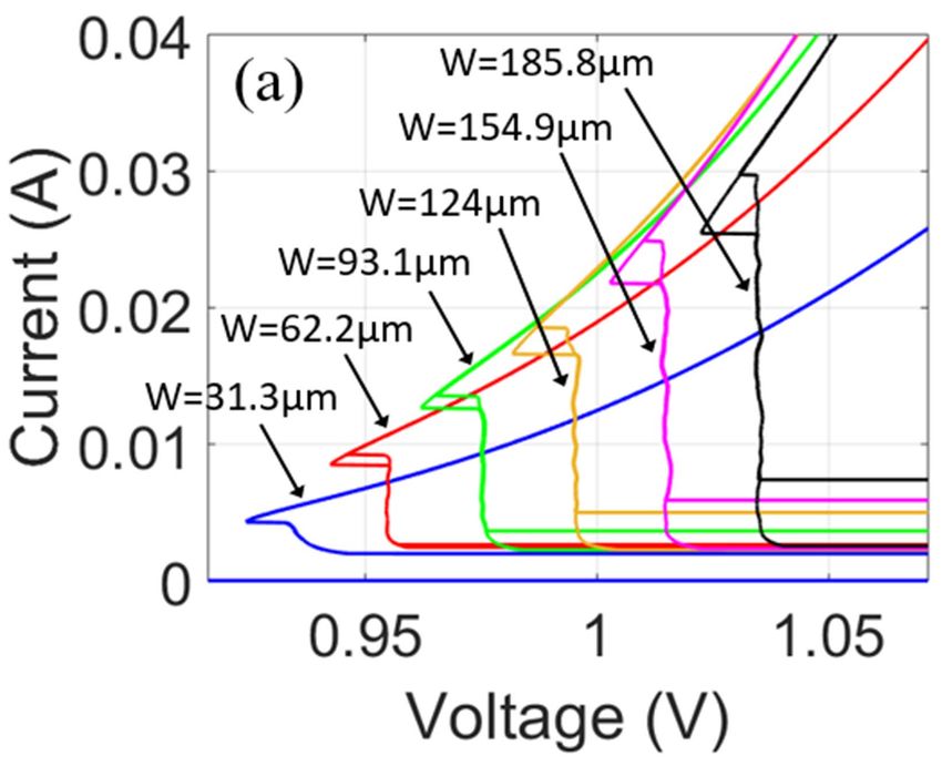
KARACA et al.: 3-D TCAD METHODOLOGY FOR SIMULATING DOUBLE-HYSTERESIS FILAMENTARY I–V BEHAVIOR 4215
What complicates matters even more is the fact that
ESD protections are usually laid out as multifinger
devices [20], [21]. I –V curves with multiple branches have
been observed in multifinger ESD protection and power
devices [17], [22], [23]. However, while the trigger current
scales with the number of fingers, the holding current is
determined from the activity of the last triggered finger when
sweeping the current down [17], [22]. Therefore, it is the
behavior of a single finger, which determines IHOLD .
In this article, we present a 3-D TCAD methodology to
investigate the double-hysteresis filamentary I –V behavior
in single-finger ESD protection SCRs and apply it to the
determination of IHOLD . The essence is to calculate the I –V
characteristics from quasi-dc up and down current sweeps
and to determine IHOLD as the smallest current where the
SCR is still in the ON-state during the down sweep. IHOLD is
analyzed as a function of layout parameters. Simulations are
compared to experimental results. We will show that IHOLD
determined from 3-D TCAD is substantially lower than that
determined from the 2-D TCAD. This has practical relevance
for protection design and excludes 2-D TCAD as a tool for
reliable IHOLD estimation.
The article is organized as follows. Section II presents
devices as well as experiments. Section III introduces the
simulation approach. Relation of filamentary I –V curves to
current density distribution over the width and the dependence
of IHOLD on layout parameters are presented and discussed in
Section IV, followed by conclusions in Section V.
II. D EVICES S TUDIED AND E XPERIMENTAL D ETAILS
Fig. 1(a) represents a simplified cross section of the studied
Fig. 1. (a) Simplified cross section of the studied device with indicated
SCRs. The structures are fabricated on low p-doped silicon on layout parameters. Devices used in 3-D TCAD analysis with (b) width-
an insulated substrate. The shallow p+ , n-well, and deep p-well extended 2-D profile and (c) edge termination. (d) Example of standard
under the Signal terminal serve as emitter (E), base (B), and mesh region (A) and region with finer mesh (B).
collector (C) of the p-n-p transistor, respectively. The n-well
III. TCAD S IMULATION A PPROACH
serves also as a substrate resistance of the p-n-p. The n+ -
contact to the n-well is short-circuited with the p+ -emitter Current density distribution and I –V curves of SCRs
by metallization. The highly doped n+ -regions of the Ground are simulated by TCAD using Synopsys Sentaurus [27].
terminal, p− -substrate/deep p-well, and n-well form the E, B, Isothermal drift-diffusion simulation is employed since the
and C regions of the n-p-n, respectively. Since the p− -substrate self-heating effect at the applied low currents is negligible
and the deep p-well are left floating, we call this device a (see Appendix). Up and down current sweeps in 3-D TCAD
floating-base SCR. The device is isolated at sides by a shallow with a rate of ±50 mA/s are used to produce the quasi-dc
trench insulation (STI). Thus, the left and right boundaries in I –V curve and reveal the possible hysteresis behavior. Since
Fig. 1(a) represent the position where STI starts. Although the solution at the next iteration step depends on the previous
the devices studied here are not exactly identical to those distribution of internal state parameters, such as current densi-
in [24], their basic structure and operation are similar. Devices ties, carrier concentrations, and electrical potential, the device
of different widths W and layout parameters L and L pn , were prehistory is well taken into account. In particular, we have
investigated [see Fig. 1(a)]. The default device parameters are monitored the current density distribution along the device
denoted by L 0 and L pn,0 . width at particular points in the up and down I –V curves
DC I –V curves were recorded in current controlled-mode in order to check whether CF was created when entering the
using a Keithley 2410 source measurement unit or HP 4155A NDR region or not. The NDR is necessary but not sufficient
semiconductor parameter analyzer. Up and down sweeps are condition to create CF [15], [16] (see more details related to
used to record the double-hysteresis I –V curve. To monitor meshing in the following and Section IV). The above is the
the current distribution over the device width as a function main approach corresponding to our TCAD methodology.
of total current, emission microscopy (EMMI) [21], [25], [26] The layouts of the 3-D simulation structures are presented
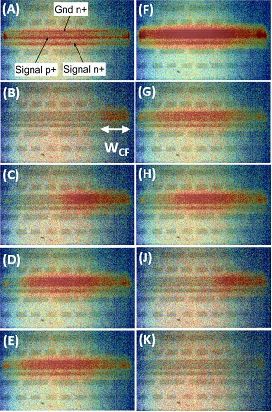
has been applied simultaneously to I –V recording. The EMMI in Fig. 1(b) and (c).
pattern is recorded from the polished backside of the chip by 1) A structure where the 2-D profile is extended in
an infrared camera [17]. the width (i.e., z-axis) direction, called here as
Authorized licensed use limited to: TU Wien Bibliothek. Downloaded on August 23,2021 at 11:14:46 UTC from IEEE Xplore. Restrictions apply.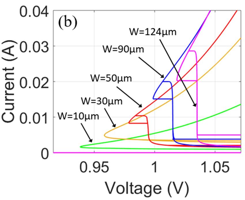
4216                                                                     IEEE TRANSACTIONS ON ELECTRON DEVICES, VOL. 68, NO. 9, SEPTEMBER 2021

       “width-extended” structure [see Fig. 1(b)], to study vari-
       ations in different W ’s, L’s, and L pn ’s. An example of
       a top view of the mesh is given in Fig. 1(d).
   2) A structure with edge terminations [see Fig. 1(c)],
       which resembles the real structure and is called “ter-
       minated” device, to investigate the effects of edges on
       the I –V curves.
   The lateral boundaries of this structure represent positions
where STI surrounds the device.
   The Neumann boundary conditions are applied at all six
sides of the simulation region. Thus, the effect of STI sur-
rounding is covered.
   To create CF when entering the NDR region in a wide
enough device, two conditions have to be fulfilled: The device
width has to be larger than about 5× the CF wall thickness
L CF [18], and there should be an inhomogeneity along the
width, which is larger than L CF [15], [16]. In our case,
L CF was about 9 μm (see the exact definition of L CF in
Section IV). In most of the simulations, the natural mesh
asymmetry created by the mesh generator [such as in region
A in Fig. 1(d)] was sufficient to induce a large enough
inhomogeneity to create a filamentary state in a wide device.
In some cases, in order to induce the filamentary instability in
devices with W > 50 μm, it was necessary to introduce an
“inhomogeneity” into the mesh, which is, in our case, a region
of about 12-μm width with a finer mesh [see region B in
Fig. 1(d)]. Thus, the widths of both regions A and B are larger
than L CF fulfilling the second condition for CF creation. The
width of region B is the same for all W values and both the
width-extended and terminated devices. From our experience,
the incommensurate ratio of mesh steps in z-direction in
regions A and B helps the convergence to stable filamentary
solution. Thus, our approach in mesh selection with respect to                 Fig. 2. Experimental I–V curves for a device with standard layout
                                                                               parameters and W = 124 µm. (a) overall and (b) zoomed-in views. The
CF creation when entering the NDR region can be summarized                     points A–K indicate the device state at which EMMI images in Fig. 4
as follows: if CF is not created for the wide enough devices                   were recorded. The current sweeping direction is indicated by arrows
(W  45 μm) with mesh of type A, we introduced the                             and color.
region B. The finer the mesh in the A and B regions, the longer
is the computational time. The mesh presented in Fig. 1(d)                     sweeping in a device with W = 124 μm. Curve “3-D”
provided sufficiently accurate and stable results. We emphasize                in Fig. 3(a) and (b) shows the up and down sweeps of
that the basic property of CF, such as L CF and general                        the 3-D TCAD simulated I –V curve in full and zoomed
shape of filamentary I –V curve, does not depend much on                       voltage scales, respectively. The I –V curve “2-D” in Fig. 3
meshing details. The mesh size determines just their accuracy.                 represents a 2-D I –V behavior with homogeneous current
In particular, the SCR properties in the ON-state (such as IHOLD               flow over the width in the NDR region. Remarkably, the
value) are quite insensitive on meshing. The more detailed                     I –V curves in Figs. 2 and 3 (curve “3-D”) both exhibit a
analysis of the meshing problem is out of the scope of this                    double-hysteresis I –V behavior. While the lower hysteresis
article and will be addressed in future work.                                  is well pronounced [see Figs. 2(a) and 3(a)], the upper one
   The simulation model is not calibrated in detail, so there is a             [see encircled regions in Figs. 2(a) and 3(a) zoomed in respec-
small deviation between the experimental and simulated I –V s.                 tive Figs. 2(b) and 3(b)] might be overlooked in the scale of
Our purpose is to concentrate on qualitative tendencies. For                   Figs. 2(a) and 3(a).
the reason of comparison, we have also performed the I –V                         Fig. 4 shows the EMMI pattern for selected points on
simulation using a 2-D TCAD with a current ramp of 50 mA/s                     the I –V curve from Fig. 2. Fig. 5 shows the 3-D plots
(rising slope). There, the simulation structure was based on the               of current density distributions for the selected points on
2-D cross section profile given in Fig. 1(a).                                  the simulated I –V curve in Fig. 3. The points are labeled
                                                                               identically in Figs. 2 and 3 according to the same qualitative
              IV. R ESULTS AND D ISCUSSION                                     behavior. However, the exact values of current and voltage
A. Double-Hysteresis I–V Behavior and IHOLD                                    can slightly differ. To clearly see the current distribution in
  Fig. 2(a) and (b) shows the measured full-scale and zoomed                   the z-direction, current density values across the line –
dc I –V curves, respectively, recorded during the up and down                  [depicted in Fig. 5(a)] were extracted and plotted in Fig. 6.

         Authorized licensed use limited to: TU Wien Bibliothek. Downloaded on August 23,2021 at 11:14:46 UTC from IEEE Xplore. Restrictions apply.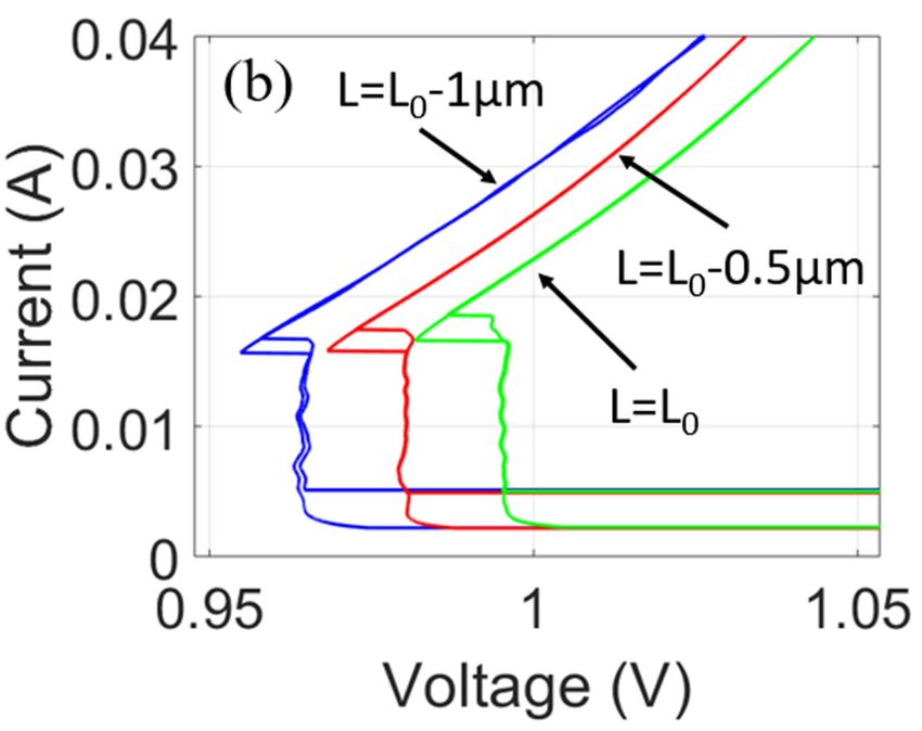
KARACA et al.: 3-D TCAD METHODOLOGY FOR SIMULATING DOUBLE-HYSTERESIS FILAMENTARY I–V BEHAVIOR                                                         4217

Fig. 3. Simulated 3-D I–V characteristics (curve “3-D”) in (a) full and        Fig. 4. EMMI images at working points A–K from Fig. 2, aligned with
(b) zoomed scales for a device with standard layout parameters and             backside reflectivity image of the device. In B, the CF width WCF is
W = 124 µm. The labels A–K indicate the working points at which                indicated.
J(z) distribution was extracted in Fig. 6. The ON-state, OFF-state and
filamentary parts of the I–V curve are indicated. The arrows indicate
the sweeping direction of the current. Curve “2-D” represents the 2-D
I–V behavior with the homogeneous current flow.                                behavior below ITR due to homogeneous current flow in this
                                                                               regime.
                                                                                  When the lateral potential drop across the p+ /n-well junc-
   At low currents of below 100 μA, a small voltage peak at                    tion at Signal is sufficiently high, the p-emitter starts to inject,
about V = 7.5 V (labeled Vnpn ) is observed in the measured                    which drives the device into the NDR region and causes
I –V curve in Fig. 2(a). It is due to avalanching and snapping-                the voltage snapback at I = ITR ≈ 5 mA [point B in
back of the open base n-p-n, which is qualitatively well repro-                Figs. 2(a) and 3(a)]. Since the simulated device is large enough
duced by simulations [see Fig. 3(a)]. The n-p-n snap-back is                   (W  L CF ), a CF can develop, resulting in the vertical or
related to the current-dependent transistor gain [28]. A small                 filamentary I –V curve at the so-called coexistence voltage
discrepancy in the Vnpn voltage in Figs. 2(a) and 3(b) is due                  UCO , Figs. 2(b) and 3(b) [11], [15]. The experimental UCO
to the noncalibrated model. The n-p-n at these small currents                  is accurately reproduced by 3-D TCAD. Note that UCO is
is turned on homogeneously over the width. We suppose                          higher than the holding voltage in the device with homoge-
that the filamentary instability due to NDR in the n-p-n is                    neous current flow, VHOLD (2-D) (see Fig. 3(b) and [11]). The
not developed due to very low current density under these                      emission pattern and J (z) at point B are shown in Fig. 4B
conditions.                                                                    and Fig. 6 (curve B), respectively. The width of this initial CF
   While the total current increases from zero up to the                       WCF of 29 μm from experiments and 20 μm from the sim-
trigger current ITR , current flows mostly via n-well substrate                ulation is consistent with its estimation from ITR /JCO , where
resistance of the p-n-p [cf. Fig. 1(a)] and the SCR remains                    JCO = ICO /W is about 0.17 and 0.25 mA/μm, respectively.
in the OFF-state. The OFF-state current flows homogeneously                    JCO is the 1-D current density, which is current independent
over the entire width [see EMMI in Fig. 4A and J (z) in Fig. 6                 along the filamentary I –V branch [11]. The CF in simulations
(curve A)]. In Fig. 3, we observe the same 3-D and 2-D I –V                    of Fig. 6 (curve B) is created and pinned at the right boundary,

         Authorized licensed use limited to: TU Wien Bibliothek. Downloaded on August 23,2021 at 11:14:46 UTC from IEEE Xplore. Restrictions apply.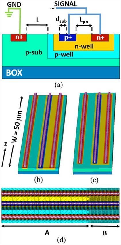
4218                                                                      IEEE TRANSACTIONS ON ELECTRON DEVICES, VOL. 68, NO. 9, SEPTEMBER 2021

                                                                                Fig. 6. Extracted distribution of simulated total current density along
                                                                                the device width at different working points (A–K) from Fig. 3. The J(z)
                                                                                distributions are extracted from data of Fig. 5, along lines such as Ω–Ω in
                                                                                Fig. 5A. The filament width WCF is indicated in curve B. The filamentary
                                                                                wall thickness LCF is indicated in curve C1.

                                                                                density OFF-state elsewhere. The J (z) distribution can be
                                                                                directly related to the distribution of the B–E voltage of the
                                                                                p-n-p transistor, which controls the SCR action. The ON- and
                                                                                OFF -state regions in the CF are separated by a transition
                                                                                region called the filamentary wall having the thickness of
                                                                                L CF (see Fig. 6 and [11], [15], and [18]). According to the
                                                                                model in [15] and [16], L CF is an increasing function of
                                                                                the conductivity of SCR base (in our case the n-well) and
                                                                                a complex function of transistor gains. The value of UCO is
                                                                                determined by the balance between the ON- and OFF-state
                                                                                regions at the filamentary wall [15], [16], [18].
                                                                                   Figs. 4C and 6 (curves C1 and C2) show the increase in
                                                                                WCF with increasing current I according to
                                                                                                                           I
                                                                                                               WCF ≈                                    (1)
                                                                                                                         JCO
                                                                                where JCO remains constant.
                                                                                   At still higher current (point D), the CF wall reaches the
                                                                                device end, and the inhomogeneous filamentary state becomes
                                                                                unstable. The current conduction reverts to a homogeneous
                                                                                state and the voltage jumps to point E. The voltage jump
                                                                                D → E represents an “energy gain” related to the disappear-
                                                                                ance of CF wall [11], [15]. The current difference dI between
                                                                                point D and the point at the ON-state I –V curve at UCO
                                                                                [see Fig. 3(b)] is related to a missing current flow over the
                                                                                region with a thickness of L CF nearly.
                                                                                   Above point E, the current flows homogeneously
Fig. 5.     3-D TCAD simulated total current density distribution in
width-extended device at working points A–K, from Fig. 3. In (C),               [see Figs. 4F and 6 (curve F)]. When the current decreases,
the working point corresponds to C1 in Figs. 3 and 6. The J(z) distribution     the homogeneous current distribution stays stable until the
is extracted along lines as Ω–Ω indicated in (A).                              point G [see Figs. 4G and 6 (curve G)]. Notice that the 3-D
                                                                                I –V (curve “3-D”) and 2-D I –V (curve “2-D”) characteristics
                                                                                in Fig. 3(b) are identical in the homogeneous ON-state. The
but a CF creation at the left one is also possible if mesh of                   upper hysteresis HDEG [see Fig. 3(b)] originates because,
type A is used over the whole device width. If a mesh of                        at point D, the parameter dI is related to L CF , while,
type B is used, then the filament originates at the side of mesh                at point G, the device enters the NDR region, which depends
type A since this region is wider than region B and the CF                      on the shape of the 2-D I –V curve. These two SCR
can develop there more easily [15], [16].                                       characteristics are not directly related to each other [15], [16].
  At UCO , the ON-state region with the high current density                    At the current region of the upper hysteresis, there may exist
JCO = ICO /W (i.e., inside the CF) coexists with a low current                  two different voltages for the same applied current depending

          Authorized licensed use limited to: TU Wien Bibliothek. Downloaded on August 23,2021 at 11:14:46 UTC from IEEE Xplore. Restrictions apply.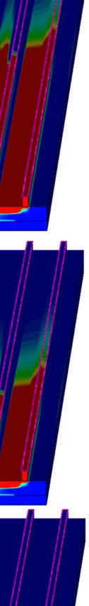
KARACA et al.: 3-D TCAD METHODOLOGY FOR SIMULATING DOUBLE-HYSTERESIS FILAMENTARY I–V BEHAVIOR                                                         4219

on whether the device conducts homogeneously over the
width (region G–E), or CF is created (H–D). These two states
depend on sweeping prehistory.
   Below point G, the device enters the NDR region, and a CF
is created. The voltage jumps to point H on the filamentary
I –V curve. The EMMI and J (z) patterns at point H show the
pronounced filamentary state [see Figs. 4H and 6 (curve H)].
Interestingly, in this simulation, the CF at point H is pinned at
the left boundary, which is the opposite side of the device
compared to the side that the current rose initially (com-
pare curves H and B–D in Fig. 6). In this particular case,
the position of mesh type B coincides with the CF position.
However, the CF can be pinned also at the right boundary,
depending on mesh details, current step, and so on, indicating
that numerical nuances matter. However, what is important is
that the CF is always created for devices larger than 50 μm
(so for W > 5 × L CF ) at either the left or right positions, and
so a stable filamentary solution is obtained.
   When the current decreases further, WCF decreases (see data
in Figs. 4 and 6 for point J) until point K, the current
called 3-D IHOLD , or IHOLD (3-D). Notice that the voltage at
point K is only slightly higher than UCO ; consider the apparent
amplifying effect of the zoomed scale in Figs. 2(b) and 3(b).
At this point, the filamentary I –V curve enters its unstable
branch (see line “F” in Fig. 1 in [11] for details). IHOLD
(3-D) is the lowest current where the SCR still operates in
the ON-state. We emphasize that this is the IHOLD value that
has to be considered in latch-up considerations. The EMMI
and J (z) in Figs. 4 and 6, respectively, show a small CF
at the structure edge at working point K. Its width WCF is
determined by L CF . L CF estimation from IHOLD (3-D)/JCO ≈
9 μm is consistent with the 20%–80% variation in J (z)
(see Fig. 6). Due to the filamentary nature of conduction,
IHOLD (3-D) of about 2 mA is much lower than IHOLD
(2-D) ≈ 20 mA. However, the current density inside the CF
of nearly JCO = 0.25 mA/μm is higher compared to that at
IHOLD (2-D) of IHOLD (2-D)/W ≈ 0.16 mA/μm. This shows
that the SCR action in CF at IHOLD (3-D) is supported by a
sufficiently high current density.                                             Fig. 7. (a) Experimental and (b) 3-D TCAD simulated I–V curves for the
                                                                               width-extended device with the device width W as a parameter. For better
   Below point K, the self-sustaining operation of SCR in the                  visibility, the curves in (a) and (b) are fanned out with a 20-mV distance
CF is not possible anymore, and the device returns to a mode                   between two curves. The VCO value for each curve does not depend on
where the current only flows through the open base n-p-n [see                  the device width W. (c) Measured and simulated IHOLD values extracted
                                                                               from data of (a) and (b). The data points for the terminated device are
point L in Figs. 2(a) and 3(a)], where the current flows again                 also included. In the case of no CF creation for W < 50 µm, the value of
homogeneously (not shown).                                                     IHOLD (2-D) is considered for IHOLD .
   We remark that the lower hysteresis LABK (see Fig. 3)
is due to the fact that, while ITR at point A is related to
homogeneous current flow in the OFF-state, the property of                        Examples of experimental and 3-D-simulated I –V curves
the SCR at point K is related to the filamentary state.                        for width-extended devices are given in Fig. 7(a) and (b),
                                                                               respectively. For better visibility, the curves for increasing
                                                                               width are subsequently horizontally fanned out with a 20-mV
B. Geometry Dependence of IHOLD                                                distance between two curves. This means that the UCO value
   The theory predicts that the filamentary instability occurs in              does not depend on the device width W . The IHOLD values
devices wider than about 5×L CF [18], which is about 45 μm                     extracted from the I –V data of Fig. 7(a) and (b) are given in
in our case. Therefore, we have carried out I –V measurements                  Fig. 7(c). In experiments, IHOLD for W = 31.3 μm is slightly
of available devices with W in the 31.3–185.8-μm range, and                    smaller than the values for W > 60 μm, which are width-
we performed simulations of both types of devices (width-                      independent. The simulated IHOLD (3-D) shows, first, a linear
extended and terminated) with W in the 2–185-μm range.                         increase with W until W = 40 μm, and then, it jumps to a
Thus, both regimes below and above 5 × L CF are covered.                       constant value for W > 45 μm. For W < 45 μm, the device

         Authorized licensed use limited to: TU Wien Bibliothek. Downloaded on August 23,2021 at 11:14:46 UTC from IEEE Xplore. Restrictions apply.
4220                                                                      IEEE TRANSACTIONS ON ELECTRON DEVICES, VOL. 68, NO. 9, SEPTEMBER 2021

Fig. 8. 3-D TCAD simulated I–V curve in width-extended and terminated
device in (a) full and (b) zoomed scales. W = 124 µm. The thick arrow
in (b) indicates the early transition from ON-state to filamentary state in
the terminated device. The small horizontal arrows indicate the current
sweeping direction.

is not large enough to induce the NDR instability, which is
consistent with the 5 × L CF criterion. For W < 45 μm,
the values of IHOLD from 2-D and 3-D TCAD are identical,
and thus, IHOLD scales linearly with W . This can be directly
seen in the I –V curves where the double-hysteresis and ideal
filamentary I –V behavior is not formed for the device with
W = 31.3 μm in experiments [see Fig. 7(a)] and for W =
10 μm and W = 30 μm in simulations [see Fig. 7(b)]. Thus,
the double-hysteresis filamentary I –V in Fig. 7(a) and (b) is
observed only for W > 5 × L CF . We notice that the lack of
devices with widths in the 30–50-μm range prevents us to see
the linearly increasing part in the IHOLD –W dependence in the
experimental data.
   Fig. 8 compares the 3-D I –V curves of the width-
extended and terminated structure for W = 124 μm. While
the trigger parameters are nearly identical for this width
[see Fig. 8(a)], IHOLD increases by 30% for the terminated
device [see Fig. 8(b)]. Furthermore, one observes a transition
from the ON-state to filamentary I –V curve at higher currents
in the down-sweep than in the terminated device, as indicated
by the thick arrow in Fig. 8(b). The termination likely induces
an inhomogeneity, which facilitates an earlier transition to the
filamentary state.                                                              Fig. 9. (a) and (b) Experimental and (c) and (d) 3-D TCAD simulated I–V
   The simulated IHOLD values in the terminated device as a                     curves for the width-extended device as a function of (a) L and (c) near
                                                                                VTR and (b) and (d) near UCO voltages. (e) Extracted measured IHOLD
function of W are added in Fig. 7(c) (see green squares). The                   and simulated values of IHOLD (3-D) and IHOLD (2-D) as a function of L.
critical device width for the CF creation of about 45 μm also
fulfills the 5 × L CF criterion. One can remark that IHOLD in                   W > 60 μm. This is attributed to an additional current flow
the terminated device is higher than that in the width-extended                 around the edge. The IHOLD values for terminated devices also
device, and this difference is nearly width-independent for                     match better to experimental values. However, this increased

          Authorized licensed use limited to: TU Wien Bibliothek. Downloaded on August 23,2021 at 11:14:46 UTC from IEEE Xplore. Restrictions apply.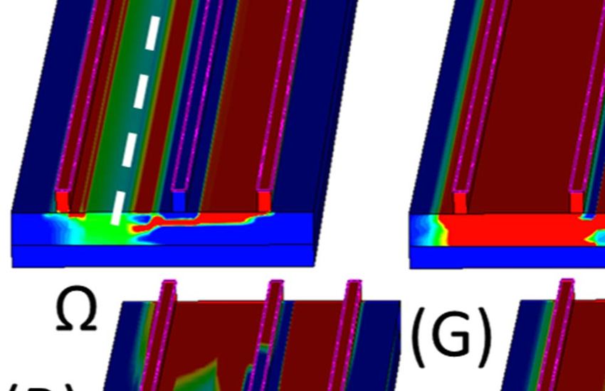
KARACA et al.: 3-D TCAD METHODOLOGY FOR SIMULATING DOUBLE-HYSTERESIS FILAMENTARY I–V BEHAVIOR                                                          4221

                                                                                layout variation, there are no experimental data. The value of
                                                                                ITR for the studied layout range does not depend much on L pn
                                                                                [see Fig. 10(a)]. ITR depends on total n-well resistance below
                                                                                p+ and in the region of length L pn [see Fig. 1(a)]. However,
                                                                                it is mainly the n-well resistance part of width dsub below the
                                                                                p-well, which controls the forward biasing of the p+ /n-well
                                                                                junction necessary for p-n-p triggering. When a potential drop
                                                                                of about 0.7 V occurs on this resistance part the SCR triggers.
                                                                                Since dsub is L pn -independent and the net n-well doping of
                                                                                this region is lower than that in the region of the length
                                                                                L pn , the value of VTR also does not depend much on L pn .
                                                                                VHOLD (2-D) decreases as L pn increases due to an increased
                                                                                contribution of the vertical p-n-p current path for larger L pn .
                                                                                The vertical current path of the p-n-p is discussed in [24].
                                                                                   The extracted values of IHOLD from 2-D and 3-D simulations
                                                                                are shown in Fig. 10(c). While IHOLD (2-D) decreases with
                                                                                L pn , IHOLD (3-D) is lower and layout-independent.
                                                                                   It is challenging to explain the independence of IHOLD
                                                                                (3-D) on layout parameters in Figs. 9(e) and 10(c) in simple
                                                                                and intuitive terms. In general, we relate it to the high injection
                                                                                condition in the CF (the SCR is in the ON-state there), where
                                                                                the details of geometry do not play a significant role. At high
                                                                                injection, a dense electron-hole plasma floods the entire device
                                                                                active region and controls the transport. In addition, in these
                                                                                floating-base devices, a conductivity modulation takes place
                                                                                in the low-doped p-sub in between the Ground n+ -region
                                                                                and deep p-well [4], [24], which complicates the picture
                                                                                even more. Moreover, although UCO , which is related to
                                                                                IHOLD (3-D), can be modeled analytically only for simple
                                                                                1-D doping profile structures [15], [16]. There is no theory,
                                                                                and therefore, the intuitive view for how UCO depends on
                                                                                the SCR structure parameters with 2-D doping profiles. The
                                                                                understanding of the complexity of this problem will be treated
                                                                                in future works.
Fig. 10. Simulated 3-D I–V curves for the width-extended device in (a) full
and (b) zoomed scales with Lpn as parameters. (c) Extracted simulated
values of IHOLD (3-D) and IHOLD (2-D) as a function of Lpn .                                                V. C ONCLUSION
                                                                                   Using quasi-dc current up and down sweeps in 3-D TCAD,
accuracy is accompanied by an increased simulation time.
                                                                                we are able to simulate the double-hysteresis I –V curve and
Since IHOLD for the width-extended device is lower than for
                                                                                holding current IHOLD in ESD protection SCRs. The shape of
the terminated device, the former represents, thus, the worst
                                                                                the I –V curve has been related to spatial distribution of the
case scenario in IHOLD estimation. For the latter and compu-
                                                                                current density in the width direction. The value of simulated
tational time-saving reasons, IHOLD for other layout variations
                                                                                IHOLD in the devices with width-extended 2-D profiles is lower
has been evaluated only for the width-extended device with
                                                                                than that in the terminated devices. The simulation of width-
W = 50 μm. For this width, a CF is certain to be created.
                                                                                extended devices represents, thus, a worst case scenario in
   Fig. 9(a)–(d) shows the experimental and simulated
                                                                                the 3-D TCAD estimation of IHOLD . IHOLD increases with the
I –V curves with L as a parameter. Fig. 9(a) and (c) shows the
                                                                                device width for W smaller than five times the filamentary
I –V curve near the VTR and Fig. 9(b) and (d) near UCO . Since
                                                                                wall thickness since no CFs are formed. For larger W , CFs
increasing L enhances the base width of the n-p-n, its gain
                                                                                are formed, and IHOLD becomes W -independent. Importantly,
decreases, and the open base breakdown voltage of the n-p-n
                                                                                while IHOLD determined from 3-D TCAD is typically indepen-
shifts slightly to higher values. As well, due to the same reason
                                                                                dent of the layout parameters, the value of IHOLD determined
the VHOLD (2-D) shifts to higher voltage with increasing L.
                                                                                from 2-D TCAD strongly depends on them and is typically
UCO follows this trend. This is observed in both experiment
                                                                                several times higher. Thus, 3-D TCAD has to be used for the
and simulation. The extracted values of IHOLD from 2-D and
                                                                                latch-up safe ESD protection design of IHOLD .
3-D simulations are given in Fig. 9(e). While IHOLD (2-D)
increases with L, IHOLD (3-D) is L-independent and much
lower than IHOLD (2-D).                                                                                            A PPENDIX
   Fig. 10(a) and (b) shows the simulated I –V curves with L pn                   The self-heating effect has been estimated using the 2-D
as a parameter near VTR and near UCO , respectively. For this                   thermodynamic simulation of the structure shown in Fig. 1(a).

          Authorized licensed use limited to: TU Wien Bibliothek. Downloaded on August 23,2021 at 11:14:46 UTC from IEEE Xplore. Restrictions apply.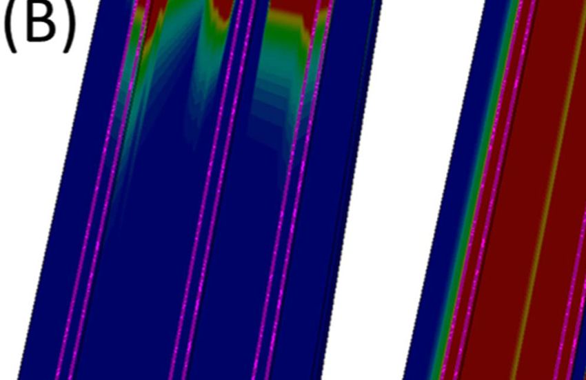
4222                                                                      IEEE TRANSACTIONS ON ELECTRON DEVICES, VOL. 68, NO. 9, SEPTEMBER 2021

STI and the additional silicon on the substrate and the lateral                 [13] K. Esmark, “Device simulation of ESD protection elements,” Ph.D.
sides have been considered. The substrate thickness was                              dissertation, ETH Zurich, Zurich, Switzerland, 2001, doi: 10.3929/ethz-
                                                                                     a-004317494.
240 μm, and the lateral chip extension beyond STI was                           [14] M. Denison et al., “Moving current filaments in integrated DMOS
200 μm on each side. The current density was chosen at                               transistors under short-duration current stress,” IEEE Trans. Elec-
JCO = ICO /W [see Fig. 3(b)], which corresponds to that in                           tron Devices, vol. 51, no. 10, pp. 1695–1703, Oct. 2004, doi:
                                                                                     10.1109/TED.2004.835978.
CF. The simulated maximum temperature rise at steady state                      [15] I. Varlamov, V. Osipov, and E. Poltoratskii, “Current fillamentation in a
was about 15 K, which represents worst case estimate. Since                          four-layer structure,” Sov. Phys. Semicond., vol. 3 no. 8, pp. 978–982,
the 2-D simulation considers zero heat flow in the z-direction                       1970.
                                                                                [16] I. V. Varlamov and V. V. Osipov, “Current filamentation in pnpn-
(i.e., infinite extended heat source in the z-direction), we may                     structures,” Sov. Phys. Semicond., vol. 3, no. 7, pp. 803–911, 1970.
expect that the temperature in the 3-D structure with finite                    [17] C. Fleury, G. Notermans, H.-M. Ritter, and D. Pogany, “TIM,
width will be even lower.                                                            EMMI and 3D TCAD analysis of discrete-technology SCRs,”
                                                                                     Microelectron. Rel., vols. 76–77, pp. 698–702, Sep. 2017, doi:
                                                                                     10.1016/j.microrel.2017.06.070.
                               R EFERENCES                                      [18] M. Meixner, P. Rodin, E. Schöll, and A. Wacker, “Lateral current
                                                                                     density fronts in globally coupled bistable semiconductors with S- or
 [1] J. Di Sarro, K. Chatty, R. Gauthier, and E. Rosenbaum, “Study of design         Z-shaped current voltage characteristics,” Eur. Phys. J. B, vol. 13, no. 1,
     factors affecting turn-on time of silicon controlled rectifiers (SCRS)          pp. 157–168, Jan. 2000, doi: 10.1007/s100510050019.
     in 90 and 65 nm bulk CMOS technologies,” in Proc. IEEE Int. Rel.           [19] M. Litzenberger, C. Furbock, D. Pogany, E. Gornik, K. Esmark, and
     Phys. Symp. Proc., San Jose, CA, USA, Mar. 2006, pp. 163–168, doi:              H. Gossner, “Investigation of 3D phenomena in the triggering of gg-
     10.1109/RELPHY.2006.251210.                                                     nMOS electrostatic discharge protection devices,” in Proc. 30th Eur.
 [2] G. Notermans et al., “Design of an on-board ESD protection for                  Solid-State Device Res. Conf., Cork, Ireland, Sep. 2000, pp. 520–523,
     USB3 applications,” IEEE Trans. Device Mater. Rel., vol. 16, no. 4,             doi: 10.1109/ESSDERC.2000.194829.
     pp. 504–512, Dec. 2016, doi: 10.1109/TDMR.2016.2622400.                    [20] C. Musshoff, H. Wolf, H. Gieser, P. Egger, and X. Guggenmos,
 [3] W. Soldner et al., “RF ESD protection strategies: Codesign vs. low-             “Risetime effects of HBM and square pulses on the failure thresholds
     C protection,” Microelectron. Rel., vol. 47, no. 7, pp. 1008–1015,              of GGNMOS-transistors,” Microelectron. Rel., vol. 36, nos. 11–12,
     Jul. 2007, doi: 10.1016/j.microrel.2006.11.007.                                 pp. 1743–1746, Nov. 1996, doi: 10.1016/0026-2714(96)00188-6.
 [4] G. Notermans, H.-M. Ritter, S. Holland, and D. Pogany, “Model-             [21] C. Russ, K. Bock, M. Rasras, I. De Wolf, G. Groeseneken, and
     ing dynamic overshoot in ESD protections,” in Proc. 40th Electr.                H. E. Maes, “Non-uniform triggering of gg-nMOSt investigated by
     Overstress/Electrostatic Discharge Symp. (EOS/ESD), Reno, NV, USA,              combined emission microscopy and transmission line pulsing,” in Proc.
     Sep. 2018, pp. 1–9, doi: 10.23919/EOS/ESD.2018.8509781.                         Electr. Overstress/ Electrostatic Discharge Symp., Reno, NV, USA,
 [5] S. H. Voldman, Latchup. Hoboken, NJ, USA: Wiley, 2008.                          Oct. 1998, pp. 177–186, doi: 10.1109/EOSESD.1998.737037.
 [6] M.-D. Ker, S.-F. Hsu, Transient-Induced Latchup in CMOS Integrated         [22] M. Gartner, D. Vietzke, D. Reznik, M. Stoisiek, K. G. Oppermann,
     Circuits. Hoboken, NJ, USA: Wiley, 2009.                                        and W. Gerlach, “Bistability and hysteresis in the characteristics of
 [7] Y.-C. Huang and M.-D. Ker, “A latchup-immune and robust SCR                     segmented-anode lateral IGBTs,” IEEE Trans. Electron Devices, vol. 45,
     device for ESD protection in 0.25-μm 5-V CMOS process,” IEEE                    no. 7, pp. 1575–1579, Jul. 1998, doi: 10.1109/16.701491.
     Electron Device Lett., vol. 34, no. 5, pp. 674–676, May 2013, doi:         [23] H. Karaca et al., “Triggering of multi-finger and multi-segment SCRs
     10.1109/LED.2013.2252456.                                                       near the holding voltage studied by emission microscopy under DC con-
 [8] M. P. Mergens, C. C. Russ, K. G. Verhaege, J. Armer, P. C. Jozwiak, and         ditions,” presented at the Int. ESD Workshop (ESDA/IEW), Hamburg,
     R. Mohn, “High holding current SCRs (HHI-SCR) for ESD protection                Germany, May 2021.
     and latch-up immune IC operation,” Microelectron. Rel., vol. 43, no. 7,    [24] H. Karaca et al., “Simultaneous and sequential triggering in multi-
     pp. 993–1000, 2003, doi: 10.1016/S0026-2714(03)00125-2.                         finger floating-base SCRs depending on TLP pulse rise time,” IEEE
 [9] H. Liang, X. Bi, X. Gu, H. Cao, and Y. Zhang, “Investigation on                 Trans. Device Mater. Rel., vol. 20, no. 4, pp. 632–640, Dec. 2020, doi:
     LDMOS-SCR with high holding current for high voltage ESD pro-                   10.1109/TDMR.2020.3033618.
     tection,” Microelectron. Rel., vol. 61, pp. 120–124, Jun. 2016, doi:       [25] K.-H. Oh, C. Duvvury, K. Banerjee, and R. W. Dutton, “Analysis of
     10.1016/j.microrel.2016.01.016.                                                 nonuniform ESD current distribution in deep submicron NMOS tran-
[10] S. Bart, B. Ilse, M. Olivier, and K. Bart, “On-chip ESD protection with         sistors,” IEEE Trans. Electron Devices, vol. 49, no. 12, pp. 2171–2182,
     improved high holding current SCR (HHISCR) achieving IEC 8 kV                   Dec. 2002, doi: 10.1109/TED.2002.805049.
     contact system level,” in Proc. IEEE Electr. Overstress/Electrostatic      [26] P. Salome, C. Leroux, J. P. Chante, P. Crevel, and G. Reimbold, “Study
     Discharge Symp. (EOS/ESD), Reno, NV, USA, Nov. 2010,                            of a 3D phenomenon during ESD stresses in deep submicron CMOS
     pp. 1–10.                                                                       technologies using photon emission tool,” in Proc. IEEE 35th Annu.
[11] D. Pogany et al., “Measuring holding voltage related to homogeneous             Int. Rel. Phys. Symp., Denver, CO, USA, Apr. 1997, pp. 325–332, doi:
     current flow in wide ESD protection structures using multilevel TLP,”           10.1109/RELPHY.1997.584282.
     IEEE Trans. Electron Devices, vol. 58, no. 2, pp. 411–418, Feb. 2011,      [27] T.C.A.D. Industry-Standard Process and Device Simulators, SENTAU-
     doi: 10.1109/TED.2010.2093143.                                                  RUS, Synopsys. Inc., Mountain View, CA, USA, May 2012.
[12] H. L. Grubin, V. V. Mitin, E. Schöll, and M. P. Shaw, The Physics          [28] B. El-Kareh and R. J. Bombard, Introduction to VLSI Silicon Devices:
     of Instabilities in Solid State Electron Devices. New York, NY, USA:            Physics, Technology and Characterization, vol. 10. New York, NY, USA:
     Springer, 2013.                                                                 Springer, 2012.

          Authorized licensed use limited to: TU Wien Bibliothek. Downloaded on August 23,2021 at 11:14:46 UTC from IEEE Xplore. Restrictions apply.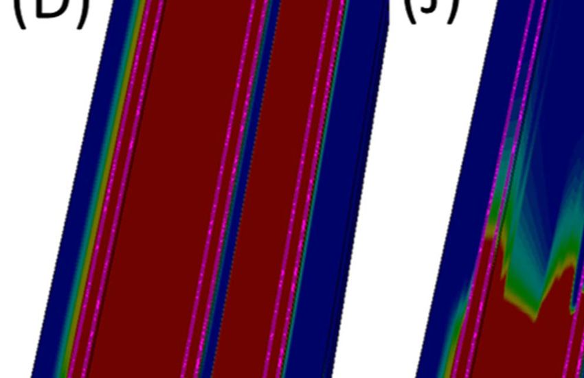
You can also read