A Fault-Tolerant and High-Speed Memory Controller Targeting 3D Flash Memory Cubes for Space Applications
←
→
Page content transcription
If your browser does not render page correctly, please read the page content below
A Fault-Tolerant and High-Speed Memory
   Controller Targeting 3D Flash Memory Cubes for
                  Space Applications
                        Anthony Agnesina1 , Da Eun Shim1 , James Yamaguchi2 , Christian Krutzik2 ,
                                  John Carson2 , Dan Nakamura3 , and Sung Kyu Lim1
                                1
                             School of ECE, Georgia Institute of Technology, Atlanta, Georgia, USA
                                  2
                                    Irvine Sensors Corporation, Costa Mesa, California, USA
                 3
                   NASA Jet Propulsion Laboratory, California Institute of Technology, Pasadena, California, USA
                                              {agnesina,daeun,limsk}@gatech.edu
                                        {jyamaguchi,ckrutzik,jcarson}@irvine-sensors.com
                                                daniel.i.nakamura@jpl.nasa.gov

   Abstract—In this work, we develop a new 3D flash memory                    they have not yet been widely adopted inside embedded
cube architecture that integrates multiple flash dies and their               systems for space, as the performance of space-qualified SSD
logic controller in a unique and optimized fashion for space                  controllers does not measure up to those of the enterprise
applications. In our Loaf-of-Bread (LOB) configuration, flash dies
are standing up and bonded laterally instead of the conventional              server and consumer markets.
pancake-style vertical die stacking. Our LOB allows the flash dies               3D memory cubes have emerged over the last few years,
to be bonded without the use of through-silicon-vias and micro-               presenting solutions to the end of Moore’s law in terms of
bumps. Instead, we insert a redistribution layer in between two               size, performance and power efficiency. Typical solutions in
adjacent dies to bring the IO signals to the bottom, where a logic
controller die collects the IOs from all flash dies and coordinates           commercial applications such as Samsung’s V-NAND [14] and
the communication with an off-cube host processor. Thus, our                  IBM’s High Bandwidth Memory [11] use vertical channels
LOB configuration allows the users to form flash memory cubes                 built into each die to connect chips together. However, the
using off-the-shelf 2D flash dies and complete the integration at             behavior and resilience of such channels in a space environ-
a packaging house instead of a fab. A key element in our LOB                  ment is yet unclear. The authors of [17] propose a space-
flash cube is the logic controller architecture that supports fault-
tolerant and energy-efficient operation of the cube. We develop               qualified NAND flash memory cube, by stacking packaged
the controller architecture and validate the functionality using              chips connected through flip chip bonding at the bottom
C++ emulation and FPGA prototyping. Compared with a state-                    of the stack. In [1], the authors explore a novel way of
of-the-art space-grade flash memory module, our system shows                  stacking, arranging the dies in a vertical fashion to allow direct
a 20X bandwidth improvement in a smaller form factor along                    individual access to the bottom edge of each die. While these
with a 25X better ratio of density per volume.
   Index Terms—Aerospace and electronic systems, Computer
                                                                              new developments make NVM much more attractive for use
architecture, Disk drives                                                     in space, the physical properties of NAND flash require a
                                                                              complex extra layer of processing and control, making their
                         I. I NTRODUCTION                                     system integration difficult.
                                                                                 However, to the best of our knowledge, no specific con-
   Advances in non-volatile memory (NVM) have led to the                      troller architecture has been proposed to take advantage of
ability of creating high density flash-based storage systems                  the new cube characteristics as well as solve reliability and
retaining information despite power loss. These systems have                  performance issues of outdated space SSD controllers. The
been readily accepted by the commercial market in the form of                 contributions of this paper are as follows:
solid-state drives (SSDs). SSDs provide high memory density
per unit volume, low power and weight without the downsides                   •   We propose a new space-qualified SSD controller micro-
of their hard disk drives counterparts (e.g. mechanical parts).                   architecture targeting 3D memory cubes that renders the
These attributes make them compelling for use in the space                        memory system reliable while retaining state-of-the-art per-
arena where more NVM applications for solid state recorders                       formance characteristics.
are being pursued. In fact, SSDs have already been used in                    •   Our novel architecture combines a flash translation layer
a few space missions, including the Mars Global Surveyor                          (FTL) controller with RTL accelerators and MRAM caching
(1996), Cassini (1997) and New Horizons (2006). However,                          to offload critical processor tasks. It also includes several
                                                                                  error mitigation enhancements to address NAND flash defi-
  This research is funded by the NASA SBIR Grant under the contract               ciencies in terms of radiation tolerance.
number NNX17CP47P. A portion of the research was carried out at the Jet       •   We design software and FPGA-based emulators to validate
Propulsion Laboratory, California Institute of Technology, under a contract
with the National Aeronautics and Space Administration.                           combined operation of the memory cube and RTL controller.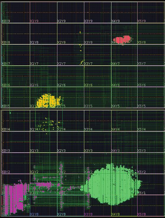
The architecture of our 3D NAND flash memory system is
                                                                      depicted in Figure 1. Individual Commercial-Off-The-Shelf
                                            memory                    (COTS) single-level cell (SLC) NAND flash and MRAM dies
                                            cube                      are stacked at wafer level in a vertical configuration. Die IOs
                                                                      are routed to the bottom of the stack on a redistribution layer
                                                                      applied on each die as shown in Figure 2. High-frequency
                                                                      bypass capacitors are incorporated in-between the dies. The
                                                  Si Filler           stack is then attached to a controller chip with integrated
                                                  Capacitor           through-silicon vias (TSV) structure to allow bumping to the
                                                  NAND flash          3D stack (top side). A typical ball grid array interface (bottom
                                                  Spare flash         side) allows the cube to be further packaged (e.g. in ceramic
                                                  MRAM                package) and connect to the underlying PCB and external host
                                                  Logic               system.
          controller          serdes              TSV                 B. Overall Controller Architecture
Fig. 1: Schematic view of our 3D NAND flash cube. The Loaf-of-           Figure 3 shows an overall view of our state-of-the-art SSD
Bread configuration allows heterogeneous stacking of COTS NAND        controller architecture centered around a logic driven imple-
and COTS MRAM dies into a single cube structure and enables           mentation and integrated in the chip sitting underneath the
individual die access for improved bandwidth and reliability.
                                                                      cube. The controller is composed of the following components:
                                                                      • A host interface connects a host computer to the SSD and
                                                                        allows multiple stacks to be chained together for scalability
                                                                        and achieve higher memory capacity.
                                                                      • A system processor implements FTL mechanisms, per-
                                                                        forming I/O requests from the host and flash management
                                                                        procedures. Many of the processor tasks are accelerated by
                                                                        offload to RTL, an easy means to improve performance,
                                                                        reliability and energy consumption without resorting to
                                                                        complex software optimizations.
                                                                      • A memory manager handles the data path, using external
Fig. 2: Completed 2-metal redistribution layer, bringing IOs to the
bottom of the die for electrically edge-connected attachment to the     MRAM to cache host data and FTL data structures.
logic controller.                                                     • A flash multiplexer/demultiplexer connects the FTL and
                                                                        MRAM cache decoupled command and data paths to each
                                                                        of the low-level NAND flash controllers.
   The rest of this paper is organized as follows. Section            • The low-level controllers communicate with the NAND flash
II reviews the overall cube and controller architectures as             chips in parallel for improved bandwidth and fault-tolerance.
well as our novel solutions to classical SSD/FTL limitations.            A processor-driven implementation as found in consumer
Section III presents RTL enhancements for built-in safety,            SSDs requires a very high-performance processor to handle
scalability and power-up performance. Section IV shows how            high bandwidth in-line data processing, which complicates
we integrate advanced memory management techniques to                 the design and increases power requirements. For this reason,
make the whole system more notably efficient and reliable. In         we develop an all-logic data path to allow a low power/low
Section V, we design a custom software emulator to confirm            resource processor to handle necessary functions. The logic
our architectural choices, we validate our RTL controller             driven implementation offers lowest power (minimize data
through simulation as well as verify the combined operation of        movement), lowest gate-count and optimal performance, at the
our custom firmware and RTL controller on a FPGA platform.            expense of flexibility and upgradeability.
Finally, conclusions are given in Section VI.
                                                                      C. Our Answers to traditional SSD Design Tradeoffs
        II. OVERVIEW OF OUR SSD A RCHITECTURE
                                                                        The SSD architecture involves many design tradeoffs. Its
A. Overall Cube Structure                                             central piece, the FTL, handles all the host commands and
   Our logic controller targets the memory cubes built using          manages the NAND flash to maximize performance, reliability
the technique developed by [1], where bare memory dies are            and endurance. It fills many duties such as the address mapping
stacked in a Loaf-of-Bread fashion. This configuration enables        of the logical block addresses (LBA) of the data from the
heterogeneous integration of different memory types such as           host to the physical page addresses (PPA) of the data in
DDR, NAND, MRAM, ReRAM or SRAM, as well as offers an                  the flash, garbage collection (GC) that frees invalid memory
individual, short and direct point-to-point interface to each die.    space, wear-leveling that spreads flash writes across the entire
This allows in particular parallelism in the execution of oper-       die to prevent premature burn-out of blocks, and bad-block
ations and individual die access for improved fault-tolerance.        management that maps out corrupt blocks. A software-only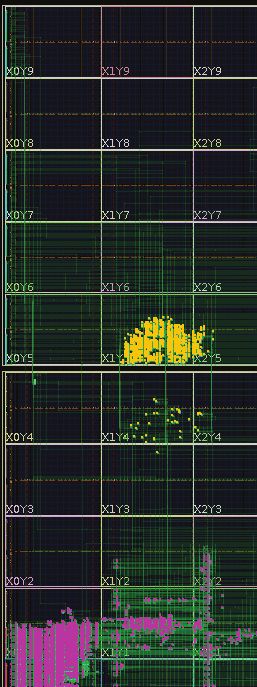
Fig. 3: Our flash-cube SSD controller architecture aiming to solve the limitations presented in Table I.

TABLE I: Our methods to increase performance, reliability and lifetime of space SSD systems, relying notably on the combination of LOB
cube structure, RTL accelerators, and MRAM caching.

        Aspect          Metrics of Interest/Limitations               Our Solutions
        Performance     Bandwidth                                     • Parallel interface of LOB structure supported by
                                                                      individual low-level controllers
                                                                      • RapidIO cube network scalability
                        Density                                       • LOB structure enabling much taller stacks
                                                                      • RapidIO cube network scalability
                        Address mapping latency                       • Accelerated hardware memory manager including caching
                        CPU processing overhead                       • Multi-level caching
                                                                      • RTL Block Merger inside each low-level controller
                        Power-up wakeup time                          • RTL bootloader
                                                                      • MRAM as main memory
        Reliability     COTS NAND radiation weaknesses                • Advanced error mitigation techniques given in Table II
                        Unsafe shutdown                               • MRAM as cache and main memory
        Lifespan        Normal wearing                                •    Hybrid-FTL offering efficient wear-leveling
                                                                      •    Data compression and scrambling
                        Write amplification                           •    Caching
                                                                      •    Hot-cold data identification

implementation typically suffers many limitations in terms of             E. Comparison
performance and safety features, as described in [2]. Table I
summarizes the main solutions that we present in the next                    Table III compares our solution with the Radiation Tolerant
sections.                                                                 and Intelligent Memory Stack (RTIMS) from 3D Plus [4],
                                                                          which was integrated on the NASA Curiosity rover for Mars
D. Our Reliability Management for Space                                   exploration. Compared with the RTIMS, our solution of-
                                                                          fers a significantly higher Density×BandWidth/Volume ratio.
   SLC NAND flash shows improved radiation tolerance to                   Table IV estimates worst case power consumption of our
total ionizing dose (20-150 krads (Si)) and single-event upset            memory solution, expected to remain under 9W. Note that
with the reducing of feature size, due to thinner oxide required          high-performance SSDs from the consumer market of similar
for the device fabrication [9]. However, heavy ion and proton             densities exhibit typical peak power consumption between 4-
irradiations still induce upsets and NAND flash is susceptible            8W. In our case, the 9W value is highly pessimistic. Indeed,
to single-event effects (SEE) on the order of 10−11 bit/day.              for example, MRAM current is heavily dependent on bank
With advanced technology nodes NAND flash reliability is                  activation rate. The worst case scenario of 100% non-repeating
indeed at risk due to fewer electrons in the flash memory                 bank access is mitigated with out-of-order execution of our
cell floating gate and larger cell-to-cell interference and dis-          MRAM memory controller. Moreover, the MRAM is mainly
turbance effects [5]. Table II shows how our 3D memory                    used for translation table lookup. Assuming sequential write
module provides robust protection against all forms of failures           access with input data rate of 800MB/s would require about
of COTS NAND flash devices, including radiation induced in                102,400 lookups per second and another 102,400 writes (as-
case of long term storage in high dose environments.                      suming all misses) which requires less than 8% active mode.
TABLE II: Our mitigation of flash error sources.

         Possible Error                                                   Our Mitigations
         Raw bit error (read and write disturb, charge loss, stuck bit,   Bose–Chaudhuri–Hocquenghem         (BCH)     error-correcting
         radiation event)                                                 codes (ECC)
         Bit error accumulation                                           Scrubbing (read, correct and rewrite data)
         Grown bad blocks                                                 Block replacement
         Die failure                                                      Enable cold spare & rebuild using redundant array of
                                                                          independent disks (RAID)
         Logical block table error                                        Reconstruct table using metadata
         SEE causing bit upset during erase or write                      Partial read-back and block/die recovery using RAID in
                                                                          case of failure
         SEE during read                                                  Embed address with CRC into spare area and validate on
                                                                          read-back
         Controller SEE                                                   Radiation hardened process & checksum for address/data
                                                                          path

TABLE III: Comparison of our solution with the RTIMS, which offers
significantly higher bandwidth in a smaller form factor.                                                        System Processor/FTL
                                                                                          Host Buffer                  Wear Leveling
    Metric                           Our cube       RTIMS [4]
                                                                                                                 Garbage Collection
    Package Size (mm)                25×25×15       28×28×10                            Microprocessor
    Density                            96GB            3GB                                                       Bad Block Manager
    #dies                                24             3
    Peak Bandwidth                    800MB/s        ∼40MB/s                                RTL                  Address Translation
    Density×BW/Volume (arb.)            8.2           0.015                              Accelerators

TABLE IV: Worst case peak active power consumption based on                          Memory Manager
values obtained from the datasheets.
                                                                                  Spare     Bootloader
         Component                             Power                              Control    SHA256
         DDR MRAM (write mode)            2×300mW [6]                             Rebuild Fault Detection
         NAND flash (write mode)         24×180mW [13]
         Cortex-M3                          20mW [3]
                                                                                   Logic    /Correction
         SerDes (4)                          1.6W [8]                                    Compressor
         Controller                             2W
         Total                                 8.5W                       Fig. 4: FTL co-software/hardware architecture. RTL accelerator mod-
                                                                          ules connect as custom Advanced High-performance Bus (AHB)
                                                                          peripherals to the CPU.
         III. DATA M ANAGEMENT I MPROVEMENTS
   Figure 4 shows the main pieces of our FTL co-software/                 NAND flash, and passed through between modules with cyclic
hardware architecture integrating a low-power microprocessor              redundancy checksums (CRC).
(ARM Cortex-M3). While we implement the more complex
tasks in software (e.g. external cache replacement policy,                B. Optimized Metadata
FTL algorithms), the entire movement (made through simple                    A spare area is dedicated in each page to store information
custom parallel interfaces with reduced signaling), protection            necessary to rebuild the FTL logical block map and related
and processing of the data is done in hardware. This requires             data structures at startup. It is also used to store health
a proper consideration of error-correcting codes, metadata                metrics such as Program/Erase (P/E) cycles. A summary of our
storage, host interface, and data hashing and compression.                advanced metadata layout is shown in Figure 5. It holds ECC
                                                                          to recover bit errors and determine which pages are valid and
A. Data & Data Path Protection                                            which blocks are failure-free. The address metadata is used by
   Data path connections are controlled in hardware and nec-              the controller to validate page reads and the address translation
essary buffering is made through FIFOs to allow for fast, low-            table. The timestamp is useful for scrubbing validation and
latency and non-stalling communications. The data is stored               identification, and a data hash serves as additional verification
with strong BCH ECC on each page of the RAM cache and                     of boot data.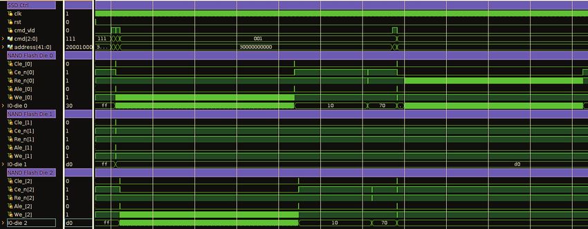
12       12           8            4        4        8          at the end of the data and instruction sections. The hash
                                                                   table stores a SHA256 checksum for each page of the code
   LBA     PPA      Timestamp Bad Block Index P/E wear
                               Marker          count               section. We accelerate the booting process by implementing
    addressing                                      FTL info       the SHA256 hash function in RTL. The system data is such
                        16          32        118                  that the P/E cycle limit of the flash is ensured by design, with
                    Metadata Hash of         Data                  no heavy writing on those pages (typically not a factory bad
                     ECC      Data           ECC                   block). Each block is 1MB in size, which allows for system
                                protection codes                   usage beyond the process code data.
                             214B                                  E. Compression
Fig. 5: Layout of metadata stored within each page, assuming 8KB     We use a hardware GZIP compression engine, based on a
page size SLC with 448B spare area and strong BCH(9130, 8192,
67) encoding of user data.                                         systolic architecture and LZ77 algorithm presented in [15].
                                                                   Compressing the data saves space and has the benefit of
                                                                   reducing write amplification and increasing write bandwidth.
                                                                   Note that not all data is compressed, and this feature is only
                                                                   used for radar imaging or audio in solid state recorders for
                                                                   example.

                                                                        IV. A HARDWARE - ONLY MEMORY MANAGEMENT
                                                                      Our hardware accelerated memory system is shown in Fig-
                                                                   ure 7. It includes components generally found in modern state-
                                                                   of-the-art microprocessor designs that are rarely put together
                                                                   in a SSD controller chip. A memory management unit (MMU)
                                                                   handles the orchestration of data movement between the FTL,
                                                                   the caches and the memory cube. Two levels of caching are
                                                                   used for better performance. First-level is a non-blocking 4-
                                                                   way associative SRAM cache with pseudo-tree least recently
                                                                   used (LRU) policy. The SRAM content is protected by a
Fig. 6: Our scalable and reliable SSD cube network architecture,   Hamming code single-error correction double-error detection
based on the space-qualified Serial RapidIO protocol. Each cube    on each of the two ports. The last-level cache is the MRAM
stores 96GB of data (24-layers).                                   which also serves as main memory for the FTL processor.
                                                                   Caching speeds up the FTL tasks where frequent mapping
                                                                   table lookups and updates are necessary (address translation,
C. A Host Interface for Reliability and Scalability                bad block, free block list, metadata for health metrics, etc.)
   The host interface logic is based on the high-speed and         and increase response time to the host for NAND bare data
fault-tolerant Serial RapidIO (SRIO) protocol. SRIO serves as      read requests (e.g. hot pages), since fetching from the flash
a standard RTL-based interface, serving similar functions as       requires more time.
SATA or NVMe, such as request scheduling. One principal
advantage of SRIO is its various fault-tolerance features. In      A. Our Address Translation Scheme
particular, it allows inter-module redundancy with no addi-           To emulate a logical disk from the host point-of-view, the
tional overhead required by the host processor, as the FTL is      FTL performs a mapping from the LBA of the host to the PPA
handled mostly by the controller of each memory module. A          inside the NAND.
scalable and reliable network of cubes is then built as shown         1) Hybrid Mapping: For mapping, we use a static scheme
in Figure 6. Technology of RAID is implemented among the           provided at a page-granularity in page order by a block
cubes, to enhance bandwidth and reliability, by spreading data     sequencing from die-to-die. On each die, we use the hybrid
and parity across multiple disks. This way, we protect from        log-structured mapping of [10] where writes are appended to
data loss in the event that one or more disks in the array fails   the next free spot in the block that is currently being written
completely. This is a valuable feature to enhance mission life     to. This way, writes are spreaded across all pages, performing
since it allows for backup modules to take-over failed modules.    wear leveling and increasing the lifetime of the devices in the
                                                                   cube.
D. RTL Bootloader                                                     2) Mapping Acceleration: A Translation-Lookaside Buffer
   A bootloader is stored as a read-only memory and preloads       (TLB) caches the last LBA-PPA mappings. In case of a miss,
the CPU instruction and data caches. For reliability and fault     a hardware Page-Table Walker (PTW) “walks” the multi-
prevention, the configuration data is stored in the lower block    level Page Table Entry (PTE) stored in the L1 cache or the
of each NAND flash with built-in ECC SHA encoding. To              MRAM to look for the mapping. If the mapping exists, it
ensure that a valid copy was decoded, a hash table is stored       automatically loads the translation into the TLB. Otherwise,
Fig. 7: Memory management in our SSD architecture, based on high-performance CPU architecture techniques.

                                                                       of the device: block table read/write operations from/to the
                                                                       NAND flash array are done only when necessary, which
                                                                       reduces write amplification. The MRAM device exhibits small
                                                                       radiation effects at the storage cell level, as well as unlimited
                                                                       endurance and extreme retention characteristics (20+ year) [7].

                                                                       C. Hot-Cold Data Identification
                                                                         We implement an efficient hot page identification scheme
                                                                       presented in [12] in RTL, originally designed for software
                                                                       implementation. It consists of two fixed-length LRU lists of
                                                                       LBAs (hot list and candidate hot list), updated based on
Fig. 8: (a) MRAM cache architecture, (b) low-level controller archi-
                                                                       write requests LBAs. This scheme is used to improve garbage
tecture.
                                                                       collection necessary to enumerate previously-used blocks that
                                                                       must be erased or recycled. Our GC policy avoids copying
the FTL is notified which in turn provides a mapping to the            hot-live data, as pages that store hot data usually have a high
never-allocated page. For robustness against SEEs, parity bits         chance of becoming invalid in the near future.
are added to the TLB contents. The TLB is also cached in
                                                                       D. Low-Level Controllers
MRAM so that the CPU can restore the corrupted state of the
TLB from the MRAM in case an error is detected.                           To obtain high bandwidth and low latency, we implement
                                                                       one channel controller per NAND device (= flash die), taking
B. MRAM Caching & Buffering                                            advantage of the LOB cube structure offering individual die
   We use the MRAM to store various controller metadata (e.g.          connections. We operate dies in parallel, i.e. they are accessed
translation table, block map table) and frequently accessed/hot        concurrently and carry out different operations independently.
pages. The organization of the MRAM cache is shown in                  This way, GC of multiple blocks are done in parallel when
Figure 8(a). State-of-the-art DRAM caches store tags in the            needed. The block diagram of each low-level controller is
DRAM itself [16]. Instead, we store tags on-chip for low               shown in Figure 8(b). When data is sent from the MMU/last-
latency of tag lookups, which in turn incurs the need of a             level cache to the controller, it is buffered in its own internal
large on-chip SRAM. Two MRAM dies are used in parallel                 queue, rather than being stalled in the cache. This provides
to protect against single event effects (the data is stored            increased performance and reduces cache accesses. Our low-
with ECC and mirrored on writes and down-selected on                   level controller architecture includes in particular the following
reads), and connected to the cache controller through a DDR4           features.
interface. The non-volatile nature of MRAM optimizes power-               1) Data Scrambling: We scramble the data so that stored
up and power-down sequencing and protects from sudden                  zeroes and ones are equally distributed to optimize binary data
power failures. These MRAM features optimize system energy             distribution. This reduces cells interference with adjacent bits
consumption, reduce the overhead of the controller (less               (read/write disturb). This also aids in an even distribution of
frequent journaling/checkpointing) and increase the lifetime           cell voltages for each bit over the lifetime of the flash, reducing
TABLE V: Design metrics of the FPGA SSD controller. The ARM
                                                                       processor and host interface are mapped onto a Cyclone V while the
                                                                       rest of the design is placed onto a Virtex Ultrascale.

                                                                                   Module             LUTs      FFs       Memory bits
                                                                                                 on Intel Cyclone V
                                                                                  Cortex-M3            22k     16.6k         3.9M
                                                                                Serial RapidIO         9.6k     10k          150K
                                                                                            on Xilinx Virtex UltraScale
                                                                             Memory Manager           14.9K    14.7K        5.5M
                                                                                Compressor             28K      46K          33K
                                                                                 SHA256               2.1K     1.8K           0
Fig. 9: Custom interface C++ software for SSD architecture testing.         24 NAND controllers        82K      39K         860K
                                                                                  Total               158K     128K         10.4M

                                                                       B. RTL Simulation & FPGA Implementation
                                                                         We perform extensive Verilog simulations of most hardware
                                                                       functions by building advanced testbenches for each module.
                                                                       Figure 11 shows correct parallel operations of the low-level
                                                                       controllers connected to NAND Verilog models from Micron.
Fig. 10: Simulation of the repair of an inconsistent block map table
at powerup.                                                            We verify the operation of the firmware with the bare-metal
                                                                       code exercising the AHB RTL peripherals correctly.
                                                                         We implement the Cortex-M3 and Serial RapidIO interface
the stress on the tunnel oxide. This in turn maximizes flash           on Intel Cyclone V due to licensing reasons. We build the
life. The scrambling and descrambling is based on a linear             prototype board shown in Figure 12 to test the processor. It
feedback shift register, which uses the LPA as a seed value            comprises a single socketed flash package connected to an
so that descrambling is possible even after a page has been            expansion header on a ARM MPS2+ board. The rest of the
moved (e.g. using internal copy-back operation).                       SSD controller including the 24 low-level controllers and RTL
   2) Block Merger: Upon exhaustion of log blocks where                accelerators is mapped onto a Xilinx XCVU440 FPGA. The
updated data is stored, the hybrid mapping requires expensive          fabric utilization of the FPGA resources is shown in Table V.
merging operations in order to allocate new log blocks. Merg-          Figure 13 shows the two aforementioned mappings.
ing will reunite pages from many blocks through page copies
and block erases and is a critical performance bottleneck. To                                  VI. C ONCLUSION
limit the CPU processing during merging that would involve                SSD performance is impacted by many design tradeoffs due
passing around large pages through the Channel Mux/Demux               to the circuit limitations of NAND flash. NAND flash also
from a NAND device to an other, we perform these expensive             suffers from reliability issues such as cell wear-out, charge
merge operations during GC inside each low-level controller            leakage, etc. These issues are intensified in the space radiation
in hardware.                                                           environment. In this work, we propose a mostly hardware
   V. V ERIFICATION OF THE PROPOSED ARCHITECTURE                       space SSD controller architecture for a new 3D NAND flash
                                                                       memory cube, where dies can be operated in parallel. The
A. Software Emulator                                                   novelty of our work is to combine a FTL controller with RTL
   In order to test the correct functioning of the FTL firmware        acceleration and MRAM cache in a single architecture. The
and help in the design of the RTL controller, we develop               enhancements we propose in terms of reliability and high-
a custom C++ trace-driven emulator of the flash controller,            speed features help SSDs stand out as the most sensible option
NAND stack with MRAM caching and SRIO daisy-chainable                  for data storage in modern interplanetary spacecraft.
interface. While executing the trace, we observe the status
of each die in the stack using the monitoring GUI shown in                                        R EFERENCES
Figure 9. This helps demonstrate functionality of our various           [1] A. Agnesina et al. A Novel 3D DRAM Memory Cube Architecture for
flash management features (firmware with GC, wear leveling,                 Space Applications. In 2018 55th ACM/ESDA/IEEE Design Automation
etc.), the capability to recover flash corruptions (e.g. rebuild            Conference (DAC), June 2018.
                                                                        [2] N. Agrawal et al. Design Tradeoffs for SSD Performance. In USENIX
table in case of power-loss scenario as shown in Figure                     2008 Annual Technical Conference, ATC’08, pages 57–70, Berkeley,
10), and optimizes memory tables and processor interaction.                 CA, USA, 2008. USENIX Association.
Furthermore, the code stores a “golden” copy of all data trans-         [3] ARM. ARM Cortex Series Documentation.
                                                                        [4] M. Bagatin et al. SEE Tests of the NAND Flash Radiation Tolerant
actions to assist debugging and perform runtime validation of               Intelligent Memory Stack. In 2015 IEEE Radiation Effects Data
operations on the cube.                                                     Workshop (REDW), July 2015.
Instruction Sequence from FTL Reading Page
die 0
die 1
die 2
Programming Page Erasing Block
Fig. 11: Simulation of the parallelism of low-level controllers, where dies are operated concurrently.
P&R processor/SRIO
P&R RTL accelerators
sha
compressor
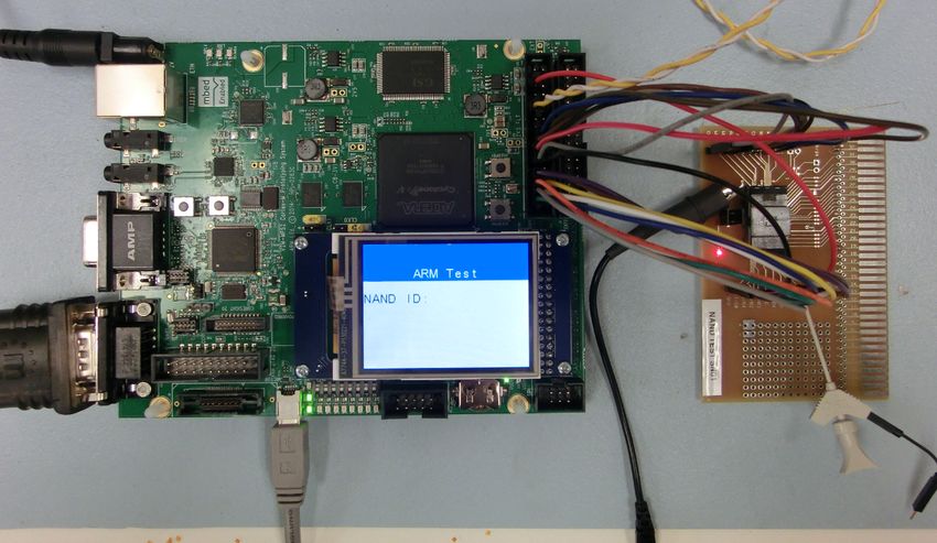
Fig. 12: Cortex-M3 based prototyping system with Cyclone-V FPGA.
[5] Y. Cai, S. Ghose, E. F. Haratsch, Y. Luo, and O. Mutlu. Errors in Flash-
Memory-Based Solid-State Drives: Analysis, Mitigation, and Recovery. low-level
ArXiv, abs/1711.11427, 2017.
memory controllers
[6] Everspin. Using MRAM to Optimize System Energy Consumption.
[7] J. Heidecker. MRAM Technology Status, 2013. system
[8] Honeywell. HXSRD02 Slider 1x/4x sRIO PHY and SERDES Quad
Transceiver Radiation Hardened. Fig. 13: FPGA layouts of SSD controller for memory cube.
[9] F. Irom et al. Single Event Effect and Total Ionizing Dose Results of
Highly Scaled Flash Memories. In 2013 IEEE Radiation Effects Data
Workshop (REDW), pages 1–4, July 2013.
[10] J. Kim et al. A space-efficient flash translation layer for CompactFlash Memory With 24-WL Stacked Layers and 50 MB/s High-Speed Pro-
systems. Consumer Electronics, IEEE Transactions on, 2002. gramming. IEEE Journal of Solid-State Circuits, Jan 2015.
[11] D. U. Lee et al. 25.2 A 1.2V 8Gb 8-channel 128GB/s high-bandwidth [15] O. Plugariu et al. FPGA systolic array GZIP compressor. In 2017
memory (HBM) stacked DRAM with effective microbump I/O test 9th International Conference on Electronics, Computers and Artificial
methods using 29nm process and TSV. In 2014 IEEE International Intelligence (ECAI), June 2017.
Solid-State Circuits Conference Digest of Technical Papers (ISSCC), Feb [16] M. K. Qureshi et al. Fundamental Latency Trade-off in Architecting
2014. DRAM Caches: Outperforming Impractical SRAM-Tags with a Simple
and Practical Design. In 2012 45th Annual IEEE/ACM International
[12] Li-Pin Chang et al. An adaptive striping architecture for flash memory
Symposium on Microarchitecture, pages 235–246, Dec 2012.
storage systems of embedded systems. In Eighth IEEE Real-Time and
[17] Tak-kwong Ng et al. Radiation tolerant intelligent memory stack
Embedded Technology and Applications Symposium, Sep. 2002.
(RTIMS). In 2nd IEEE International Conference on Space Mission
[13] Micron. NAND Flash Die 32Gb Die: x8 300mm SLC, MT29F32G08AB. Challenges for Information Technology (SMC-IT’06), July 2006.
[14] K. Park et al. Three-Dimensional 128 Gb MLC Vertical nand FlashYou can also read