Aerosol Jet Printing of Silver Lines with A High Aspect Ratio on A Heated Silicon Substrate - Mdpi
←
→
Page content transcription
If your browser does not render page correctly, please read the page content below
materials
Article
Aerosol Jet Printing of Silver Lines with A High
Aspect Ratio on A Heated Silicon Substrate
Alexey Efimov * , Pavel Arsenov * , Denis Kornyushin, Anna Lizunova, Ivan Volkov
and Victor Ivanov
 Moscow Institute of Physics and Technology (National Research University), Dolgoprudny 141701, Russia;
 kornush94@rambler.ru (D.K.); anna.lizunova@gmail.com (A.L.); volkov256@yandex.ru (I.V.);
 ivanov.vv@mipt.ru (V.I.)
 * Correspondence: arsenov@phystech.edu (P.A.); efimov.aa@mipt.ru (A.E.)

 Received: 19 November 2019; Accepted: 4 February 2020; Published: 5 February 2020

 Abstract: In this work, we studied the formation of conductive silver lines with high aspect ratios (AR =
 thickness/width) > 0.1 using the modernized method of aerosol jet printing on a heated silicon substrate.
 The geometric (AR) and electrical (resistivity) parameters of the formed lines were investigated
 depending on the number of printing layers (1–10 layers) and the temperature of the substrate
 (25–300 ◦ C). The AR of the lines increased as the number of printing layers and the temperature of
 the substrate increased. An increase in the AR of the lines with increasing substrate temperature was
 associated with a decrease in the ink spreading as a result of an increase in the rate of evaporation of
 nano-ink. Moreover, with an increase in the substrate temperature of more than 200 ◦ C, a significant
 increase in the porosity of the formed lines was observed, and as a result, the electrical resistivity of
 the lines increased significantly. Taking into account the revealed regularities, it was demonstrated
 that the formation of silver lines with a high AR > 0.1 and a low electrical resistivity of 2–3 µΩ·cm is
 advisable to be carried out at a substrate temperature of about 100 ◦ C. The adhesion strength of silver
 films formed on a heated silicon substrate is 2.8 ± 0.9 N/mm2 , which further confirms the suitability
 of the investigated method of aerosol jet printing for electronic applications.

 Keywords: aerosol nanoparticles; printed electronics; aspect ratio; microstructure; sintering; silver;
 electrical resistivity; 3D manufacturing

1. Introduction
     Currently, there is great interest in the manufacture of low-cost electronic devices using printing
technologies [1,2]. The use of these technologies allows the formation of active and passive components by
direct deposition of functional materials in the form of nanoparticles on the surface of the substrate without
the use of expensive photolithographic masks and stencils [3–6]. Among the existing printing methods,
aerosol jet printing is the most promising technology because it allows the formation of functional
elements with a minimum lateral size of up to 10 microns [7–9] both on flat and curved substrates [10,11].
This technology has been applied for the manufacture of transistors [12], sensors [13–15], solar cells [16],
microheaters [17], microantennas [18,19] and interconnects [20]. Previous studies of this technology
relied mainly on the formation of thin-film microstructures due to the need for the manufacture of
planar electronic devices. At the same time, there is a large and inevitable production demand for
the manufacture of narrow and abnormally high bulk microstructures having aspect ratios (ratio of
thickness to line width) of more than 0.1. These microstructures, for example, are relevant for use
as busbars and fingers of solar cells, where minimization of dimming losses due to narrow line widths
and minimization of power losses due to high line thicknesses are required [21].

Materials 2020, 13, 730; doi:10.3390/ma13030730                                 www.mdpi.com/journal/materials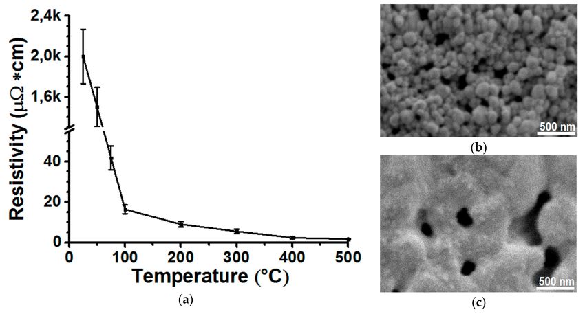
Materials 2020, 13, 730                                                                                       2 of 12

      There are not many studies reporting the study of ways to increase the aspect ratio of lines formed
by aerosol jet printing. Therefore, earlier in the work [22], it was established that in a single-pass
mode of aerosol printing due to the optimization of rates of aerosol and sheath gas, it is possible to
obtain narrow (20 µm) lines with an aspect ratio of more than 0.1. At the same time, it was shown
in [23], that an increase in the number of print passes and a decrease in the speed of movement of
the substrate do not lead to an increase in the aspect ratio of the lines due to the effect of ink spreading
during aerosol jet printing. Obtaining lines with a high aspect ratio is possible only using additional
approaches for processing the substrate or the deposited material. Therefore, one of the approaches is
to structure the substrate using imprinting or lithography, which limits the spreading of ink on it [24],
and the second approach is based on the use of multiple printing passes in combination with local
laser sintering of the deposited material [25–28]. Both presented approaches significantly complicate
and increase the cost of the aerosol jet printing process through the use of additional lithographic,
laser and optomechanical equipment.
      In this regard, there is still a need to develop and study more technologically simple methods
that ensure the formation of lines with a high aspect ratio. Therefore, in this paper, we proposed
to investigate a fairly simple method of aerosol jet printing of lines on a thermally heated substrate,
in which the conditions for forming lines with a high aspect ratio will be ensured due to the temperature
effect on the deposited material and many printing passes. In addition, in this work, a comparative study
of the geometric parameters, structure, morphology, and electrical resistivity of lines of nanoparticles
deposited on an unheated and heated substrate with the potential of their use as current-carrying
compounds will be performed.

2. Experimental
     In the experiments, the formation of the studied lines was carried out on a modernized commercial
aerosol jet printer AJ 15XE (Neotech AMT GmbH, Nuremberg, Germany). The modernization of
the aerosol jet printer was to provide controlled heating of the substrate in the process of aerosol
printing using heating plate in the temperature range from 25 to 500 ◦ C. The experimental setup,
including a modernized aerosol jet printer for the deposition of silver lines on a heated silicon substrate,
is shown in Figure 1.

      Figure 1. Schematic of an experimental setup for focused deposition of aerosol particles on a heated
      silicon substrate (a); An example of a cross-sectional profile of a silver line, measured with an optical
      profilometer, where the measured thickness t, width W and aspect ratio AR of the line are ~ 67 µm, ~
      43 µm and 0.64, respectively. The characteristic lengths of the formed lines in the experiments ranged
      from 10 to 30 mm. The inset shows the optical image of this line (b).

    Aerosol particles in the form of micro droplets with nanoparticles inside were generated using
a pneumatic atomizer during spraying a mixture of silver nano-ink PG-007 (Paru Co. Ltd., Seoul,
South Korea) based on solvents 1-methoxy-2-propanol (MOP) and ethylene glycol (EG) in a volume
Materials 2020, 13, 730                                                                                       3 of 12

ratio of 3:1, respectively. The sheet resistivity of the sintered nano-ink layer was 3.5 mΩ/sq according
to the manufacturer's specification [29]. The mass concentration of silver nanoparticles in the ink was
about 46%. Nanoparticles had a size in the range from 5 to 420 nm with a mean size of 108 ± 68 nm
according to the results of measurements by transmission electron microscope JEM-2100 (JEOL Ltd.,
Tokyo, Japan). Pure nitrogen N2 (99.9999%) was used as the carrier gas. Next, the aerosol particles
were transport to a print head with a micro nozzle for focusing and deposition on a moving heated
silicon substrate. In the experiments, a micro nozzle with an outlet diameter of 150 µm was used,
and the distance from the micro nozzle to the substrate was 5 mm. The line was deposited when
the substrate was moved relative to the nozzle with a constant printing speed of the order of V s =
100 mm/min. The characteristic lengths of the formed lines in the experiments ranged from 10 to 30 mm.
The control of the line width W was carried out by changing the values of the focusing ratio (FR =
Qsh /Qa ) with varying flow rates of aerosol Qa and constant sheath gas Qsh = 90 sccm. The possibility of
increasing the thickness of the formed lines was achieved due to several layers of printing on each other
in the multi-pass mode. In this case, the temperature of the substrate was a critical parameter, since it
affected the spreading of nano-ink due to a change in the drying rate, evaporation, and solidification of
the nano-ink.
      Experiments to determine the conditions and patterns of silver line formation with a high aspect
ratio and low resistivity were performed in two stages. At the first stage, a study was made of
the temperature ranges responsible for the drying and sintering of the deposited silver nano-ink in
order to obtain monolithic lines with a low resistivity. To do this, we studied the dependence of
the electrical resistivity of silver lines on heat treatment of nano-ink in the range from 25 to 500 ◦ C,
and also established the nature of the dependence of the measured resistance on temperature in
the range from 25 to 100 ◦ C for sintered and dried lines. Sintered lines were those that were dried
and sintered, and dried lines were those that had only been dried. In this case, the drying process
involved the removal of the solvent and surfactants included in the composition of the used nano-ink,
and the sintering process was responsible for monolithization of the deposited nano-ink.
      At the second stage, we studied the effect of the number of printing layers N (from 1 to 10)
and the temperature of the heated substrate Ts (from 25 to 300 ◦ C) on the values of width W, thickness t,
aspect ratio AR and electrical resistivity ρ, as well as structural and morphological features of the formed
lines. The values of the variable and fixed parameters of the aerosol jet printing process used in
the experiments are presented in Table 1. In the process of aerosol jet printing on a heated substrate in
several layers, each subsequent layer was deposited immediately after printing of the previous layer
without additional exposure to time. In this case, experiments on printing lines on a heated substrate
were carried out with completely heated substrate. The total heating time of the substrate was from 10
to 20 min, depending on the set temperature. After the process of aerosol jet printing, the obtained
lines were additionally sintered on a heating plate at a temperature of 400 ◦ C for 60 minutes in order to
ensure their conductive properties.

      Table 1. Parameters of the aerosol jet printing process to establish the effect of the number of printing
      layers N and the temperature of the heated substrate Ts on the characteristics of the lines formed.

        Number of Printing       Substrate Temperature         Printing Speed V s
                                                                                         Focusing Ratio FR
           Layers N                     T s (◦ C)                  (mm/min)
               1, 2, 5, 10                25, 100                      100                        5
                   10              25, 50, 100, 200, 300               100                        2

     In order to demonstrate the effect of ink spreading on the substrate the FR = Qsh /Qa was reduced
from 5 to 2 in experiments to establish the effect of the Ts (25, 50, 100, 200 and 300 ◦ C) on the aspect
ratio of lines (see Table 1). The value of the FR was reduced due to an increase in the amount of aerosol
Qa deposited on the substrate at Qsh = const. Moreover, earlier in [22] it was already shown that
increasing the value of the FR allows increasing the values of the aspect ratio of the printed lines.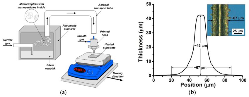
Materials 2020, 13, 730                                                                             4 of 12

     The aspect ratio (AR) of the lines was determined from the analysis of the cross-sectional profile
of the line in accordance with Equation (1):

                                                      t
                                               AR =     ,                                              (1)
                                                      W
where t – line thickness, W – line width.
     The line cross-sectional profile was measured using a DCM 3D optical profilometer
(Leica Microsystems GmbH, Wetzlar, Germany). This profilometer allows to obtain an averaged
cross-sectional profile of lines. The profile was averaged over 50 lines section with an analysis
area of 200 × 200 µm2 . As an example, Figure 1b shows the measured line cross-sectional profile
for which a thickness t ~ 43 µm, a width W ~ 67 µm, and an aspect ratio of the line AR ~ 0.64
were determined. The electrical resistivity of the lines ρ was determined using Equation (2):

                                                   S
                                                ρ=R ,                                                  (2)
                                                   L
where R – line resistance, S – line cross-sectional area, L – line length.
      The line resistance R was measured using the four-point probe method [30]. For this purpose,
four contacts were formed on the surfaces of the silver lines using conductive silver paste PELCO®#
16031 (Ted Pella, Inc., Redding, CA, USA). A current I in the range of 10 to 100 µA was passed through
two external contacts using a current source SourceMeter 2401 (Tektronix, Inc., Beaverton, OR, USA).
The voltage drop V between two internal contacts was measured using a U1253B multimeter
(Agilent Technologies, Inc, Santa Clara, CA, USA). Based on the measurement data, I was obtained
as a function of V, which had a linear character and from which the resistance of printed lines R was
calculated as the slope of I(V) plot. The cross-sectional area of line S was measured using an optical
profilometer DCM 3D (Leica Microsystems GmbH, Wetzlar, Germany), and the line length L was
measured using an optical microscope VHX-1000 (KEYENCE Corp. of America, Itasca, IL, USA).
The structural and morphological features of the lines were determined using a JSM 7001F scanning
electron microscope (JEOL, Ltd., Tokyo, Japan).
      In order to confirm the suitability of using a thermally heated substrate in the process of aerosol
jet printing, we measured the adhesion strength of silver films with an area of 15x15 mm2 formed on
a heated silicon substrate at Ts = 100 ◦ C, N = 5 layers, FR = 2, and V s = 1000 mm/min and sintered
at 400 ◦ C for 60 minutes. The adhesion measurements were carried out using a pull-off adhesion
analyzer LUMiFrac (LUM GmbH, Berlin, Germany) according to ISO 4624 [31]. The glue Super Moment
(Henkel Rus, Ltd., Moscow, Russia) was used as an adhesive between printed layer and pull off test
stamp with bonded area of 78.5 mm2 . The glued parts were cured at room temperature for 12 hours
according to the manufacturer's datasheet. The samples of this study have been tested with a linear
load increase of 5 N/s and a temperature of 25 ◦ C. Fourteen samples were analyzed in pull off test.
The tensile strength σ [32] are calculated using the centrifugal force Fc and the bonded area A by
the following Equation (3):
                                                 σ = Fc/A,                                            (3)

    Thus, based on the results of the studies, regularities for the formation of lines on a heated
substrate were established and conditions that ensure the production of lines with a high aspect ratio
and minimum electrical resistivity were found.

3. Results and Discussion
     Lines with high aspect ratios (AR = thickness/width) are required for many applications in printed
electronics [22]. In addition, the lines must have a low resistivity required to minimize resistive losses
in manufactured electronic devices [33,34]. The low resistivity of the lines of nanoparticles is ensured
when the nanoparticles are continuously connected to each other, and the bulk structure of the line
Materials 2020, 13, 730                                                                                            5 of 12

has a low porosity [35]. As a rule, this is achieved by thermal drying and subsequent sintering of
the deposited lines, provided that the nanoparticle structure is densely formed [35,36]. Therefore,
in the drying process at relatively low temperatures < 150 ◦ C, the solvent and surfactants are removed
from the surface of the nanoparticles, and in the process of sintering of the nanoparticles at high
temperatures > 250 ◦ C, the formation of many contacts between nanoparticles takes place, and a bulk
monolitic structure is formed [37].
      In aerosol jet printing of lines on a heated substrate, depending on its temperature Ts , the processes
of deposition, spreading, drying, and sintering of nanoparticles can occur in parallel. For this reason,
the substrate temperature Ts can significantly affect both the aspect ratio AR of the formed lines due to
the influence on the spreading, drying and evaporation rates of the nano-ink, and their morphology,
structure and deposition density of nanoparticles, and, as a consequence, on the electrical resistivity of
the lines. Considering this, before the experiments on the deposition of lines on a heated substrate,
the study investigated the effect of heat treatment used nano-ink on resistivity ρ, conductivity, structure
and morphology of the lines in order to determine the temperature ranges responsible for the drying
and sintering processes.
      Figure 2a shows the temperature dependence of the electrical resistivity ρ of the line of silver
nano-ink in the range from 25 to 500 ◦ C during the heat treatment. The error bars shown in Figure 2a
are the expanded uncertainty determined from the measurements of 10 lines with a 95% confidence
probability [38]. The formation of this line was carried out at Ts = 25 ◦ C, N = 1 layer, FR = 5 and V s =
100 mm/min. It is shown from Figure 2 that the electrical resistivity ρ of the initial thermally untreated
line at 25 ◦ C is extremely high and amounts to ~ 2000 µΩ·cm. In this case, a significant drop in
the line electrical resistivity by two orders of magnitude from ~ 2000 to ~ 16 µΩ·cm is achieved with
increasing temperature from 25 to 100 ◦ C, respectively. At a temperature of about 100 ◦ C, the drying
process of the line is probably completed as a result of evaporation of the main fraction of the solvent
mixture (1-methoxy-2-propanol and ethylene glycol) and decomposition of the organic surfactants
included in nano-ink. Confirmation of this statement is presented in Figure 2b, where the SEM image
of the surface of the line heat-treated at 100 ◦ C shows that the line surface has a structure consisting of
many individual micro-sized agglomerates of nanoparticles weakly bonded to each other, which is
typical for dried structures from nanoparticles.

      Figure 2. Dependence of the electrical resistivity of the lines from silver nano-ink on the temperature of
      the substrate heating (a); SEM image of a line dried at 100 ◦ C (b) and sintered at 400 ◦ C (c), respectively.
      The formation of the lines was carried out at Ts = 25 ◦ C, N = 1 layer, FR = 5 and V s = 100 mm/min.
Materials 2020, 13, 730 6 of 12
Figure 2a also shows that with a further increase in the heating temperature from 100 to 300 ◦ C,
the electrical resistivity of the line changes less significantly from ~ 16 to ~ 6 µΩ·cm, respectively.
This temperature range is probably responsible for the beginning of the stage of the sintering process
of nanoparticles, at which contacts and necks between nanoparticles begin to form. Moreover, it can
also be seen from the graph in Figure 2a that the complete sintering of nanoparticles occurs in
the temperature range from 300 to 500 ◦ C, where the line electrical resistivity reaches minimum values
of the order of ~ 2.3 µΩ·cm and then ceases to change with increasing substrate temperature [39,40].
In the SEM image of the surface of the line heat-treated at 400 ◦ C, it can be seen that the line consists of
a bulk monolitized material with a certain number of micro-sized pores formed during sintering of
nanoparticles. These structural features and line morphology are characteristic of sintered nanoparticle
structures, where the presence of pores in the line structure also causes a nearly 2-fold difference
between the electrical resistivity of the sintered silver line and the bulk silver resistivity of 1.6 µΩ·cm.
Thus, by analyzing the dependence of the electrical resistivity of the line of nanoparticles on
the heating temperature of the substrate (Figure 2a), it was found that the drying and sintering
processes used by the nanoparticles are completed at temperatures of approximately 100 ◦ C and 400 ◦ C,
respectively. An additional confirmation of this statement is the results of measurements of the nature
of the temperature dependence of the heat-treated lines at 100 ◦ C and 400 ◦ C for 60 min, respectively.
In Figure 3, the samples dried at 100 ◦ C and sintered at 400 ◦ C demonstrate a different character of
the dependence of resistance on temperature.
Figure 3. Temperature dependence of the resistance of dried and sintered lines after heat treatment for
60 minutes formed at temperatures of 100 ◦ C (a) and 400 ◦ C (b), respectively. The formation of this
lines was carried out at Ts = 25 ◦ C, N = 1 layer, FR=5 and V s = 100 mm/min.
The error bars shown in Figure 3a,b are the expanded uncertainty determined
from the measurements of ten lines with a 95% confidence probability. The resistance of the dried
samples has a semiconductor nature of conductivity, since it decreases exponentially with increasing
temperature, see Figure 3a. Figure 3a shows that with increasing line temperature from 25 to 100 ◦ C,
the resistance of the dried lines decreases from 18 to 0.3 kΩ, respectively. In this case, the resistance of
sintered lines increases linearly from 6.6 to 8.0 Ω with an increase in the line temperature from 25 to
100 ◦ C (Figure 3b), which is a characteristic for metal structures.
Subsequently, the established temperature ranges responsible for the drying and sintering of
particles were used in experiments of aerosol jet printing on a heated substrate in order to obtain lines
with a high aspect ratio and low electrical resistivity.
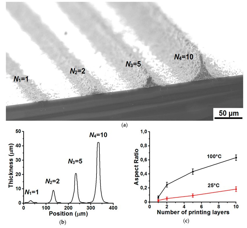
Figure 4a shows SEM images of silver lines formed by aerosol jet printing on a heated silicon
substrate at Ts = 100 ◦ C, V s = 100 mm/min and FR = 5, depending on the number of printing layers N =
1, 2, 5, and 10. The lines after printing were additionally sintered on a heating plate at a temperature of
400 ◦ C for 60 minutes in order to ensure their conductive properties. Figure 4b shows their respectiveMaterials 2020, 13, 730 7 of 12
cross-sectional profiles. Figure 4a,b show that with an increase in the number of printing layers N
from 1 to 10 when particles are deposited on a heated substrate at Ts = 100 ◦ C, the thickness of the lines
t increases from ~ 2 to ~ 43 µm with a change in their width W from ~ 37 to ~ 66 µm, respectively.
This increase is probably due to the fact that when printing on a heated substrate during the deposition
of ink material on a heated surface, the ink dries quickly, without having time to spread on the surface,
and the subsequent layer of ink material is deposited already on the annealed line.
From the analysis of the cross-sectional profiles of the lines shown in Figure 4b, the aspect ratio
AR of the lines was determined and their dependence on the number of printing layers N (1–10) was
plotted when printing on a heated substrate at Ts = 100 ◦ C, see Figure 4c. A similar analysis was also
performed for lines formed on an unheated substrate at Ts = 25 ◦ C. Figure 4c shows that the aspect ratio
of the lines formed on the heated substrate at Ts = 100 ◦ C almost linearly increases with the number of
printing layers N. For example, AR values increase from 0.06 to 0.63 with an increase in the number of
printing layers N is from 1 to 10, respectively. In this case, the electrical resistivity ρ of the sintered
lines is ~ 2.4 µΩ·cm.
Figure 4. SEM image of silver lines formed by aerosol jet printing on heated silicon substrate at Ts
= 100 ◦ C with a change in the number of printing layers N from 1 to 10, where V s = 100 mm/min
and FR = 5 (a) and their relevant cross-sectional profiles measured on an optical profilometer (b).
The dependence of the values of the aspect ratio of lines on the number of printing layers N is from 1 to
10 when printing on heated substrate at Ts = 100 ◦ C and on unheated substrate at Ts = 25 ◦ C (c).Materials 2020, 13, 730 8 of 12
In case of printing on unheated substrate at Ts = 25 ◦ C, the absolute values of the aspect ratio AR
of lines reach lower values in comparison with the printing mode on heated substrate at Ts = 100 ◦ C.
For example, the aspect ratio of the lines is 0.18 and 0.63 at a temperature of the heated substrate
of 25 ◦ C and 100 ◦ C, respectively. This indicates that during the deposition of lines on unheated
substrate, due to a greater spreading, the nano-ink along with an increase in the line thickness t
due to a larger amount of deposited material substantially increases its width W in accordance with
the expression AR = (thickness/width). Thus, it was experimentally found that using a heated substrate
Ts = 100 ◦ C and a multitude of printing layers, it is possible to multiply increase the aspect ratio of
lines in proportion to the number of layers N.
However, for a number of practical applications, it is not enough just to have lines with a high
aspect ratio. It is also required that the lines have a low electrical resistivity ρ. Since the temperature of
the heated substrate Ts in the process of aerosol jet printing, in addition to the aspect ratio, can also affect
the spreading, drying, and sintering rates of the nano-ink, and as a result, the structure and morphology
of the line and its electrical resistivity ρ. For this reason, the influence of the temperature of the heated
substrate Ts in the range from 25 to 300 ◦ C on the aspect ratio AR, resistivity ρ, morphology, and line
structure was investigated.
Figure 5a shows a SEM image of lines formed by aerosol jet printing on heated substrate, depending
on the substrate temperature Ts equal to 25 ◦ C, 50 ◦ C, 100 ◦ C, 200 ◦ C, and 300 ◦ C at N = 10 layers, V s =
100 mm/min and FR = 2. In comparison with the previous experiment, the focusing ratio was reduced
to 2 in order to demonstrate the effect of ink spreading on the substrate by increasing the amount of
aerosol Qa deposited on the substrate at Qsh = const. The relevant cross-sectional profiles of the formed
lines are shown in Figure 5b. The lines after printing were additionally sintered on a heated plate
at a temperature of 400 ◦ C for 60 minutes in order to ensure their conductive properties. The measured
values of electrical resistivity ρ, aspect ratio AR, width W, thickness t and cross-sectional area of lines S
depending on the temperature of the heated substrate Ts are presented in Table 2.
Figure 5. SEM image of lines formed by the method of aerosol jet printing on heated substrate,
depending on the substrate temperature Ts equal to 25 ◦ C, 50 ◦ C, 100 ◦ C, 200 ◦ C, and 300 ◦ C at N
= 10 layers, V s = 100 mm/min and FR = 2 (a); Relevant line cross-section profiles measured with
an optical profilometer (b).
Figure 5a,b show that the temperature of the heated substrate Ts during aerosol jet printing
has a significant effect on the geometry of the formed lines. Figure 5a shows that when aerosol jet
printing of lines in the multi-pass mode at N = 10 layers, when the substrate temperature is Ts = 25 ◦ C,
a significant spreading of nano-ink is observed and, as a result, the lines are wide W ~ 250 µm and have
low aspect ratio AR ~ 0.020, see Table 2. At the same time, it can also be seen from Figure 5b and Table 2
that even with a slight increase in the temperature of the heated substrate from 25 to 50 ◦ C, a significant
change in the geometry of the line is observed, namely, its width decreases significantly from ~ 250
to ~ 134 µm, and the thickness varies from ~ 5 to ~ 15 µm, which ultimately leads to an increase inMaterials 2020, 13, 730 9 of 12
the aspect ratio AR of the line from 0.02 to 0.11, respectively. This increase in the aspect ratio of the line
is probably due to an increase in the contact angle θ due to a change in the composition of the nano-ink
due to their evaporation upon deposition on a heated substrate. An increase in the contact wetting
angle θ with an increase in the substrate temperature was previously studied in [41] in the process
of capillary printing of chemical sensors. In work [41] It was found that the contact wetting angle
θ can vary over a wide range from 30◦ to > 90◦ depending on the temperature Ts and the printing
speed V s , and thus, to a large extent, determine the geometry of the formed lines from nano-ink.
A schematic representation of the influence of the wetting angle θ on the geometry of the formed lines
of nanomaterials with increasing temperature is shown in the inset in Figure 5b. The inset shows that,
with an increase in the contact angle θ, a decrease in the width W and an increase in the thickness t of
microdroplets on the surface are observed. In our experiments, as the substrate temperature increases
from 100 to 300 ◦ C, as in the work [41] due to the increase in the rate of evaporation of the nano-ink,
the contact wetting angle θ is also likely to increase further, and as a result, there is a further increase
in the aspect ratio of the lines from 0.17 to 0.70, respectively (see Figure 5b and Table 2).
Table 2. Parameters of the aerosol jet printing process to establish the effect of the number of print
layers N and the temperature of the heated substrate Ts on the characteristics of the lines formed.
T s (◦ C) 25 50 100 200 300
ρ (µΩ·cm) 2.96 ± 0.28 2.69 ± 0.28 2.56 ± 0.24 3.53 ± 0.32 6.98 ± 0.73
AR 0.020 ± 0.004 0.11 ± 0.02 0.17 ± 0.03 0.47 ± 0.08 0.70 ± 0.12
t (µm) 5.1 ± 0.9 15.2 ± 2.1 23.1 ± 3.2 46.9 ± 6.3 62.6 ± 8.4
W (µm) 250.3 ± 23.6 134.2 ± 15.1 135.5 ± 14.6 99.1 ± 10.2 90.6 ± 9.4
S (µm2 ) 1170 ± 234 970 ± 175 1280 ± 225 1462 ± 249 2072 ± 352
It was also found that with increasing temperature of the heated substrate Ts in the range from 100
to 300 ◦ C, the electrical resistivity of the formed lines increases from 2.56 ± 0.24 to 6.98 ± 0.73 µΩ·cm,
respectively (see Table 2). This increase in the electrical resistivity ρ can be explained by an increase in
the porosity of the lines, due to the too rapid evaporation of the microdroplets of nano-ink at elevated
temperatures in the range of 200–300 ◦ C. An indirect confirmation of this statement is an increase in
the cross-sectional area S of the lines from 1280 ± 225 to 2072 ± 352 µm2 with an increase in the substrate
temperature from 100 to 300 ◦ C, respectively (see Table 2). It is known that the amount of material
deposited, which is proportional to the cross-sectional area of line S, should not depend on the substrate
temperature Ts . In this regard, it can be assumed that the increase in the cross-sectional area of the line
S observed with increasing substrate temperature Ts is associated with an increase in the porosity of
the formed lines. Thus, it was found that too high temperatures of the heated substrate Ts > 200 ◦ C
lead to the formation of lines with high values of electrical resistivity.
In this regard, we can conclude that in the process of aerosol printing on a heated substrate in
the multi-pass mode in order to form lines with a high aspect ratio and low resistivity, an optimal choice
of substrate temperature is required. The optimum temperature of the substrate should contribute
to a decrease in the spreading of the nano-ink and exclude the formation of a porous line structure,
affecting their electrical and mechanical properties.
According to the results of adhesive tests, it was found that the adhesive strength of silver films
formed on a heated silicon substrate at the optimum temperature Ts = 100 ◦ C is 2.8 ± 0.9 N/mm2 .
This value of adhesive strength is sufficient for use in electronics with a high safety factor [42]. Thus,
the suitability of the use of a heated substrate in the process of aerosol jet printing for the formation of
conductive and adhesive-strong structures is further confirmed.Materials 2020, 13, 730 10 of 12
4. Conclusions
In this work, we studied the formation of silver lines on a heated silicon substrate during aerosol jet
printing with varying the number of printing layers 1–10 and the temperature of the substrate 25–300 ◦ C
in order to obtain lines with a high aspect ratio > 0.1 and low electrical resistivity. As the deposited
material, commercial silver nano-ink with a mass content of nanoparticles of about 46% was used.
The temperature values responsible for the drying and sintering process of the nano-ink, which were
100 and 400 ◦ C, respectively. It is established that the values of the aspect ratio of the line obtained
during printing on a heated substrate at 100 ◦ C are several times higher than under conditions of
using an unheated substrate. It has also been found that the aspect ratio of the lines increases linearly
with the number of print layers. In addition, it was found that with an increase in the temperature of
the substrate from 25 to 100 ◦ C, due to a decrease in the spreading of the nano-ink and an increase in
the contact angle, there is a substantial increase in the aspect ratio of the formed lines from 0.02 to 0.17,
respectively. Moreover, a further increase in the temperature of the substrate from 100 to 300 ◦ C, in
addition to increasing the aspect ratio of the lines from 0.17 to 0.70, due to an increase in the porosity
of the structure, leads to an increase in the electrical resistivity from 2.56 to 6.98 µΩ·cm, respectively.
According to the results of adhesive tests, it was found that the approach of aerosol jet printing on
a heated substrate is suitable for electronic applications, since the adhesive strength of silver films
was 2.8 N/mm2 . Thus, it has been experimentally shown that the formation of silver lines with a high
aspect ratio > 0.1 and a low resistivity of 2-3 µΩ·cm is advisable to be carried out at a substrate
temperature of about 100 ◦ C.
Author Contributions: Conceptualization, P.A., A.E. and I.V.; Data curation, D.K.; Formal analysis, D.K., A.E.;
Investigation, P.A., A.L.; Methodology, A.E.; Project administration, V.I.; Supervision, A.E. and V.I.; Validation,
P.A.; Visualization, D.K.; Writing – original draft, P.A., A.E. All authors have read and agreed to the published
version of the manuscript.
Funding: This work was supported by the Russian Science Foundation (project # 19-79-00375).
Conflicts of Interest: The authors declare no conflict of interest.
References
1. Garlapati, S.K.; Divya, M.; Breitung, B.; Kruk, R.; Hahn, H.; Dasgupta, S. Printed Electronics Based on
Inorganic Semiconductors: From Processes and Materials to Devices. Adv. Mater. 2018, 30, 1707600.
[CrossRef] [PubMed]
2. Subramanian, V.; Chang, J.B.; de la Fuente Vornbrock, A.; Huang, D.C.; Jagannathan, L.; Liao, F.; Mattis, B.;
Molesa, S.; Redinger, D.R.; Soltman, D.; et al. Printed electronics for low-cost electronic systems: Technology
status and application development. In Proceedings of the ESSCIRC 2008 - 34th European Solid-State Circuits
Conference; 2008; pp. 17–24. [CrossRef]
3. Maeng, S.-Y.; Lee, D.-K.; Choi, J.-W.; Kim, H.-J.; Kang, C.-Y.; Nahm, S.; Yoon, S.-J. Design and fabrication of
multilayer actuator using floating electrode. Mater. Chem. Phys. 2005, 90, 405–410. [CrossRef]
4. Rivadeneyra, A.; Loghin, F.C.; Falco, A. Technological Integration in Printed Electronics. Flex. Electron. 2018.
[CrossRef]
5. Efimov, A.A.; Arsenov, P.V.; Volkov, I.A.; Urazov, M.N.; Ivanov, V.V. Study of aerosol jet printing with dry
nanoparticles synthesized by spark discharge. J. Phys. Conf. Ser. 2017, 917, 092020. [CrossRef]
6. Kumar, L.; Islam, T.; Mukhopadhyay, S.C. Sensitivity Enhancement of a PPM Level Capacitive Moisture
Sensor. Electronics 2017, 6, 41. [CrossRef]
7. Seifert, T.; Sowade, E.; Roscher, F.; Wiemer, M.; Gessner, T.; Baumann, R.R. Additive Manufacturing
Technologies Compared: Morphology of Deposits of Silver Ink Using Inkjet and Aerosol Jet Printing. Ind.
Eng. Chem. Res. 2015, 54, 769–779. [CrossRef]
8. Arsenov, P.V.; Efimov, A.A.; Ivanov, V.V. Effect of Methods of Changing in Focusing Ratio on Line Geometry
in Aerosol Jet Printing. Key Eng. Mater. 2018, 779, 159–164. [CrossRef]
9. Protas, N.V.; Efimov, A.A.; Zemlyanoy, V.K.; Ivanov, V.V. Computer simulation of aerosol nanoparticles focusing
and deposition process for functional microstructure fabrication. J. Phys. Conf. Ser. 2018, 1124, 081033. [CrossRef]Materials 2020, 13, 730 11 of 12
10. Borghetti, M.; Serpelloni, M.; Sardini, E. Printed Strain Gauge on 3D and Low-Melting Point Plastic Surface
by Aerosol Jet Printing and Photonic Curing. Sens. 2019, 19, 4220. [CrossRef]
11. Jabari, E.; Toyserkani, E. Aerosol-Jet printing of highly flexible and conductive graphene/silver patterns.
Mater. Lett. 2016, 174, 40–43. [CrossRef]
12. Hong, K.; Kim, S.H.; Mahajan, A.; Frisbie, C.D. Aerosol Jet Printed p- and n-type Electrolyte-Gated Transistors
with a Variety of Electrode Materials: Exploring Practical Routes to Printed Electronics. ACS Appl. Mater.
Interfaces. 2014, 6, 18704–18711. [CrossRef] [PubMed]
13. Vasiliev, A.A.; Varfolomeev, A.E.; Volkov, I.A.; Simonenko, N.P.; Arsenov, P.V.; Vlasov, I.S.; Ivanov, V.V.;
Pislyakov, A.V.; Lagutin, A.S.; Jahatspanian, I.E.; et al. Reducing Humidity Response of Gas Sensors for
Medical Applications: Use of Spark Discharge Synthesis of Metal Oxide Nanoparticles. Sensors 2018, 18.
[CrossRef] [PubMed]
14. Vasiliev, A.; Varfolomeev, A.; Volkov, I.; Arsenov, P.; Efimov, A.; Ivanov, V. Gas Sensor with Reduced Humidity
Response Based on Metal Oxide Nanoparticles Synthesized by Spark Discharge. Orient. J. Chem. 2018,
34, 648–654. [CrossRef]
15. Tortorich, R.P.; Shamkhalichenar, H.; Choi, J.-W. Inkjet-Printed and Paper-Based Electrochemical Sensors.
Appl. Sci. 2018, 8, 288. [CrossRef]
16. Mette, A.; Richter, P.L.; Hörteis, M.; Glunz, S.W. Metal aerosol jet printing for solar cell metallization.
Prog. Photovolt. Res. Appl. 2007, 15, 621–627. [CrossRef]
17. Arsenov, P.V.; Vlasov, I.S.; Efimov, A.A.; Minkov, K.N.; Ivanov, V.V. Aerosol Jet Printing of Platinum
Microheaters for the Application in Gas Sensors. IOP Conf. Ser. Mater. Sci. Eng. 2019, 473, 012042. [CrossRef]
18. Yuxiao, H.; Oakley, C.; Chahal, P.; Albrecht, J.; Papapolymerou, J. Aerosol Jet printed 24 GHz end-fire
quasi-Yagi-Uda antenna on a 3-D printed cavity substrate. In Proceedings of the 2017 International Workshop
on Antenna Technology: Small Antennas, Innovative Structures, and Applications (iWAT), Athens, Greece,
1–3 March 2017; pp. 179–182. [CrossRef]
19. Cai, F.; Pavlidis, S.; Papapolymerou, J.; Chang, Y.H.; Wang, K.; Zhang, C.; Wang, B. Aerosol jet printing
for 3-D multilayer passive microwave circuitry. In Proceedings of the 2014 44th European Microwave
Conference, Rome, Italy, 6–9 October 2014; pp. 512–515. [CrossRef]
20. Elmogi, A.; Soenen, W.; Ramon, H.; Yin, X.; Missinne, J.; Spiga, S.; Amann, M.-C.; Srinivasan, A.; De Heyn, P.;
Van Campenhout, J.; et al. Aerosol-Jet Printed Interconnects for 2.5 D Electronic and Photonic Integration.
J. Light. Technol. 2018, 36, 3528–3533. [CrossRef]
21. Bag, S.; Deneault, J.R.; Durstock, M.F. Aerosol-Jet-Assisted Thin-Film Growth of CH3NH3PbI3 Perovskites—A Means
to Achieve High Quality, Defect-Free Films for Efficient Solar Cells. Adv. Energy Mater. 2017, 7, 1701151. [CrossRef]
22. Mahajan, A.; Frisbie, C.D.; Francis, L.F. Optimization of aerosol jet printing for high-resolution, high-aspect
ratio silver lines. ACS Appl. Mater. Interfaces. 2013, 5, 4856–4864. [CrossRef]
23. Kopola, P.; Zimmermann, B.; Filipovic, A.; Schleiermacher, H.-F.; Greulich, J.; Rousu, S.; Hast, J.; Myllylä, R.;
Würfel, U. Aerosol jet printed grid for ITO-free inverted organic solar cells. Sol. Energy Mater. Sol. Cells 2012,
107, 252–258. [CrossRef]
24. Chu, T.-Y.; Zhang, Z.; Tao, Y. Printing Silver Conductive Inks with High Resolution and High Aspect Ratio.
Adv. Mater. Technol. 2018, 3, 1700321. [CrossRef]
25. Kocabas, C.; Meitl, M.A.; Gaur, A.; Shim, M.; Rogers, J.A. Aligned arrays of single-walled carbon nanotubes
generated from random networks by orientationally selective laser ablation. Nano. Lett. 2004, 4, 2421–2426.
[CrossRef]
26. Renn, M.J.; Schrandt, M.; Renn, J.; Feng, J.Q. Localized Laser Sintering of Metal Nanoparticle Inks Printed
with Aerosol Jet®Technology for Flexible Electronics. J. Microelectron. Electron. Packag. 2017, 14, 132–139.
[CrossRef]
27. Khabarov, K.; Kornyushin, D.; Masnaviev, B.; Tuzhilin, D.; Saprykin, D.; Efimov, A.; Ivanov, V. The Influence
of Laser Sintering Modes on the Conductivity and Microstructure of Silver Nanoparticle Arrays Formed by
Dry Aerosol Printing. Appl. Sci. 2020, 10, 246. [CrossRef]
28. Khabarov, K.M.; Kornyushin, D.V.; Masnaviev, B.I.; Tuzhilin, D.N.; Efimov, A.A.; Saprykin, D.L.; Ivanov, V.V.
Laser sintering of silver nanoparticles deposited by dry aerosol printing. J. Phys. Conf. Ser. 2019, 1410, 012217.
[CrossRef]
29. PRINTED ELECTRONICS. Available online: https://www.iparu.com/printed-electronics (accessed on
24 January 2020).Materials 2020, 13, 730 12 of 12
30. Vogeler, F.; Verheecke, W.; Voet, A.; Valkenaers, H. Aerosol Jet®printed interconnections on extrusion based
3D printed substrates. In International Conference on Polymers and Moulds Innovations (PMI); Ghent, Belgium,
12–14 September 2012.
31. ISO 4624: 2016 (en). Paints and varnishes - Pull-off test for adhesion. Available online: https://www.sis.se/
api/document/preview/920202/ (accessed on 5 February 2020).
32. Rietz, U.; Lerche, D.; Hielscher, S.; Beck, U. Centrifugal Adhesion Testing Technology (CATT) - A Valuable
Tool for Strength Determination. J. Adhesion Soc. Jap. 2015, 51, 293–297. [CrossRef]
33. Laurent, P.; Stoukatch, S.; Dupont, F.; Kraft, M. Electrical characterization of Aerosol Jet Printing (AJP)
deposited conductive silver tracks on organic materials. Microelectron. Eng. 2018, 197, 67–75. [CrossRef]
34. Efimov, A.A.; Minkov, K.N.; Arsenov, P.V.; Protas, N.V.; Ivanov, V.V. Investigation of sintering of silver lines
on a heated plastic substrate in the dry aerosol jet printing. J. Phys. Conf. Ser. 2018, 1124, 081041. [CrossRef]
35. Wünscher, S.; Abbel, R.; Perelaer, J.; Schubert, U.S. Progress of alternative sintering approaches of
inkjet-printed metal inks and their application for manufacturing of flexible electronic devices. J. Mater.
Chem. C. 2014, 2, 10232–10261. [CrossRef]
36. Lefky, C.; Mamidanna, A.; Huang, Y.; Hildreth, O. Impact of solvent selection and temperature on porosity
and resistance of printed self-reducing silver inks. physica status solidi (a) 2016, 213, 2751–2758. [CrossRef]
37. Kim, D.; Moon, J. Highly Conductive Ink Jet Printed Films of Nanosilver Particles for Printable Electronics.
Electrochem. Solid-State Lett. 2005, 8, J30–J33. [CrossRef]
38. ISO/IEC Guide 98-3:2008(en). Uncertainty of measurement — Part 3: Guide to the expression of uncertainty in
measurement (GUM:1995). Available online: https://www.sis.se/api/document/preview/910301/ (accessed on
5 February 2020).
39. Efimov, A.A.; Arsenov, P.V.; Protas, N.V.; Minkov, K.N.; Urazov, M.N.; Ivanov, V.V. Dry aerosol jet printing
of conductive silver lines on a heated silicon substrate. IOP Conf. Ser. Mater. Sci. Eng. 2018, 307, 012082.
[CrossRef]
40. Lizunova, A.A.; Efimov, A.A.; Arsenov, P.V.; Ivanov, V.V. Influence of the sintering temperature on morphology
and particle size of silver synthesized by spark discharge. IOP Conf. Ser. Mater. Sci. Eng. 2018, 307, 012081.
[CrossRef]
41. Kahng, S.-J.; Cerwyn, C.; Dincau, B.M.; Kim, J.-H.; Novosselov, I.V.; Anantram, M.P.; Chung, J.-H. Nanoink
bridge-induced capillary pen printing for chemical sensors. Nanotechnol. 2018, 29, 335304. [CrossRef]
[PubMed]
42. Ratautas, K.; Jagminienė, A.; Stankevičienė, I.; Sadauskas, M.; Norkus, E.; Račiukaitis, G. Evaluation
and optimization of the SSAIL method for laser-assisted selective electroless copper deposition on dielectrics.
Results Phys. 2020, 16, 102943. [CrossRef]
© 2020 by the authors. Licensee MDPI, Basel, Switzerland. This article is an open access
article distributed under the terms and conditions of the Creative Commons Attribution
(CC BY) license (http://creativecommons.org/licenses/by/4.0/).You can also read