An innovative architecture for a wide band transient monitor on board the HERMES nano-satellite constellation
←
→
Page content transcription
If your browser does not render page correctly, please read the page content below
An innovative architecture for a wide band transient monitor
                                                   on board the HERMES nano-satellite constellation
                                                  F. Fuschinoa,b , R. Campanaa,b , C. Labantia,b , Y. Evangelistac,d , F. Fioree , M. Gandolaf ,
                                                M. Grassig , F. Melef , F. Ambrosinoc , F. Ceraudoc , E. Demenevh , M. Fiorinil , G. Morgantea ,
                                                   R. Piazzollac , G. Bertucciof , P. Malcovatig , P. Belluttih,m , G. Borghih,m , G. Dililloo,n ,
                                                   M. Ferocic,d , F. Ficorellah,m , G. La Rosai , P. Nogarai , G. Paulettao,n , A. Picciottoh,m ,
                                              I. Rashevskayam , A. Rachevskin , G. Sottilei , A. Vacchio,n , E. Virgillia , G. Zampan , N. Zampan ,
                                                               N. Zorzih,m , T. Chenp , N. Gaop , J. Caop , Y. Xup , and L. Wangp
arXiv:2101.03035v1 [astro-ph.IM] 8 Jan 2021

                                                                     a
                                                                           INAF/OAS, Via Gobetti 101, I-40129, Bologna, Italy
                                                         b
                                                             INFN–Sezione di Bologna, Viale Berti Pichat 6/2, I-40127, Bologna. Italy
                                                               c
                                                                 INAF/IAPS Roma, Via Fosso del Cavaliere 100, I-00133, Roma, Italy
                                                            d
                                                              INFN-Tor Vergata, Via della Ricerca Scientifica, 1 I-00133, Roma - Italy
                                                                       e
                                                                         INAF/OATS, Via G.B. Tiepolo 11, I-34143, Trieste, Italy
                                              f
                                                Department of Electronics, Information and Bioengineering (DEIB) of Politecnico di Milano,
                                                                            Como Campus, Via Anzani 42, 22100 Como, Italy
                                                g
                                                  Department of Electrical, Computer, and Biomedical Engineering, University of Pavia, Via
                                                                                    Ferrata 5, 27100, Pavia, Italy
                                                          h
                                                            Fondazione Bruno Kessler – FBK, Via Sommarive 18, I-38123 Trento, Italy
                                                  i
                                                    INAF, Istituto di Astrofisica Spaziale e Fisica cosmica di Palermo, via U. La Malfa 153,
                                                                                        I-90146 Palermo, Italy
                                                                   l
                                                                     INAF-IASF Milano, Via Alfonso Corti 12, I-20133 Milano, Italy
                                                                         m
                                                                           TIFPA-INFN, Via Sommarive 14, I-38123 Trento, Italy
                                                   n
                                                     INFN Italian National Institute for Nuclear Physics c/o Area di Ricerca Padriciano 99,
                                                                                         I-34127 Trieste, Italy
                                                o
                                                  Department of Mathematics, Computer Science and Physics University of Udine, Via delle
                                                                                   Scienze 206, I-33100 Udine, Italy
                                                       p
                                                         Institute of High Energy Physics, Chinese Academy of Sciences, Beijing, China

                                                                                             ABSTRACT
                                              The HERMES-TP/SP mission, based on a nanosatellite constellation, has very stringent constraints of sensitivity
                                              and compactness, and requires an innovative wide energy range instrument. The instrument technology is based
                                              on the “siswich” concept, in which custom-designed, low-noise Silicon Drift Detectors are used to simultaneously
                                              detect soft X-rays and to readout the optical light produced by the interaction of higher energy photons in
                                              GAGG:Ce scintillators. To preserve the inherent excellent spectroscopic performances of SDDs, advanced readout
                                              electronics is necessary. In this paper, the HERMES detector architecture concept will be described in detail,
                                              as well as the specifically developed front-end ASICs (LYRA-FE and LYRA-BE) and integration solutions.
                                              The experimental performance of the integrated system composed by scintillator+SDD+LYRA ASIC will be
                                              discussed, demonstrating that the requirements of a wide energy range sensitivity, from 2 keV up to 2 MeV, are
                                              met in a compact instrument.
                                              Keywords: Nanosatellites, constellation, Gamma-ray Burst, Silicon Drift Detectors, Scintillator Detectors
                                                Send correspondence to:
                                                Fabio Fuschino, E-mail: fabio.fuschino@inaf.it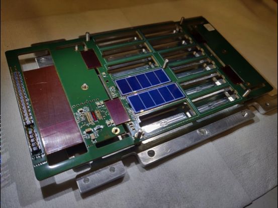
1. INTRODUCTION
Gamma-Ray Bursts (GRBs) are one of the most intriguing and challenging phenomena for modern science,
because of their huge luminosities, up to more than 1052 erg/s, their redshift distribution extending from z ∼ 0.01
up to z > 9. Their study is of very high interest for several fields of astrophysics, such as the physics of matter in
extreme conditions, cosmology, fundamental physics and the mechanisms of gravitational wave signal production.
    The High Energy Modular Ensemble of Satellites - Technologic and Scientific Pathfinder (HERMES-TP/SP)1
is a new mission concept hosting compact but innovative X-ray detectors for the monitoring of cosmic high energy
transients, such as Gamma Ray Bursts and the electromagnetic counterparts of Gravitational Wave events, based
on a constellation of six 3U nanosatellites. The main topic of HERMES is to demonstrate that accurate location
of high energy cosmic transients can be obtained using CubeSats. That means miniaturized hardware, one
order of magnitude smaller costs than conventional space observatories and few years of development time. The
four pillars of the HERMES project are: 1) providing a first mini-constellation for GRB localization with a
total of six units, for GRB triangulation using miniaturized and distributed instrumentation, joining also to the
multimessenger revolution; 2) develop miniaturized payload technology for breakthrough science; 3) contribute to
the so-called Space 4.0 goals demonstrating that components off-the shelf (COTS) can be reliable for challenging
missions; 4) push and prepare for final and more solid larger constellation.
    The HERMES-TP project is funded by the Italian Ministry for education, university and research and the
Italian Space Agency. The HERMES-SP project is funded by the European Union’s Horizon 2020 Research
and Innovation Programme under Grant Agreement No. 821896. The constellation should be tested in orbit
in 2022. HERMES-TP/SP is intrinsically a modular experiment that can be naturally expanded to provide a
global, sensitive all sky monitor for high energy transients.

                                   2. HERMES MISSION CONCEPT
The HERMES approach differs from the conventional idea to build increasingly larger and expensive instruments.
HERMES proposes to realize distributed, modular and innovative instruments composed by tens/hundreds of
simple units, cheaper and with a limited development time. The current CubeSat technologies demonstrated
that off-the-shelf components for space use can offer solid readiness at a limited cost. The physical dimension of
a single HERMES detector need to be compliant with the nanosatellite mechanical structure; the 1U CubeSat
standard is 10×10×10 cm3 . Therefore, the single HERMES detector is of course under-performing, having a lower
effective area when compared with transient monitors currently operating. The lower costs and the innovative
concept of distributed instrument demonstrate that to build an new mission with unprecedented sensitivity is
actually feasible. The HERMES detector is designed to provide a sensitive area >50 cm2 , suggesting that with
several tens/hundreds of such units a total sensitive area of the order of magnitude of ∼1 m2 can be reached.
By measuring the time delay between different satellites, using cross correlation of the lightcurves detected by
different satellites,2 the localisation capability of the whole constellation is directly proportional to the number
of components and inversely proportional to the average baseline between them. As a rough example, with a
reasonable average baseline of ∼7000 km, represented by the Earth radius, and a reasonable number for low-
Earth satellites in suitable orbits (e.g. ∼100 nanosats) simultaneously detecting a transient, a source localisation
accuracy of the order of magnitude of ∼10 arcsec2 can be reached, for transients with milliseconds time scale
variability.
   A more extensive description of HERMES mission concept is given in other proceedings in this volume.2–4

                                      3. PAYLOAD DESCRIPTION
A sketch of the HERMES payload, allocated in 1U-CubeSat (10×10×10 cm3 ), is shown in Figure 1. A mechanical
support is placed on the instrument topside. The support is composed by two parts to hold an optical/thermal
filter. The detector core is located under the mechanical support: this is a scintillator-based detector in which
Silicon Drift Detectors (SDD5 ) are used to both detect soft X-rays, by direct absorption in silicon, and to
simultaneously readout the scintillation light. The payload unit is expected to allocate a detector with >50
cm2 sensitive area in the energy range from 2 keV up to 2 MeV, with a total power consumption
electronics, power supply and data handling functionalities. They are allocated on the bottom of the payload
unit, below the detector unit. A more extensive description of HERMES payload is given in other proceedings
in this volume.6

Figure 1. Exploded view of the payload unit (10×10×10 cm3 ) on board the HERMES nanosatellite. From the top are
shown the mechanical support composed by top and bottom parts, with optical filter (violet) in middle, the FEE board
(dark green) allocating SDD matrices (light green), LYRA-FE chips on the top and LYRA-BE chips folded on the side
(not shown for clarity), the GAGG:Ce crystal pixels and their housing. A mechanical rib on top is also visible, necessary
to fix the whole payload to the satellite structure.

                               4. DETECTOR CORE ARCHITECTURE
The HERMES detector is based on the so-called “siswich” concept,7, 8 exploiting the dual intrinsic sensitivity
of silicon to both soft X-rays and scintillation light. Thus, aiming at designing a compact instrument with a
very wide sensitivity band, the silicon detectors are optically coupled with inorganic scintillators. The detector
is therefore composed by an array of scintillator pixels, optically insulated, read out by SDDs.
    In this concept the SDDs play also the role of an independent X-ray solid state detector. When the SDD
faces the sky, low energy X-rays are directly absorbed by the SDD, while higher energy X-rays and γ-rays,
pass through the silicon sensor without interactions and are absorbed in the scintillator crystal. The optical
scintillation photons are than collected by the same silicon sensor. Only very low noise readout devices coupled
with state-of-the-art front-end electronics allow to reach a low energy scintillator threshold down to 20–30 keV.
This is a key issue of this architecture, considering that around these energies the increasing sensitivity of the
scintillator is able to compensate the lack of efficiency of thin silicon wafers (450 µm), so a quite flat overall
sensitivity in a wide energy band for the whole integrated system is reached. This effect is clearly visible in the
Figure 2 where both silicon and scintillator detection efficiency vs. photon energy are shown.
   The inorganic scintillator selected for HERMES is the Cerium-doped Gadolinium-Aluminum-Gallium Garnet
(GAGG:Ce).9 This is a very promising material with high light output (∼50 000 ph/MeV), a fast radiation
decay time of ∼90 ns, no hygroscopicity, high density (6.63 g/cm3 ) with an effective mean atomic number of
54.4, no internal radioactive background, peak light emission at 520 nm. These specifications make this material
very suitable for the HERMES detector. Since GAGG:Ce is a relatively recent crystal, it has not been yet
extensively investigated with respect to radiation resistance and performance after irradiation, although the
published results are very encouraging.10 Further radiation tests were carried out by our collaboration, to better
understand the scintillator behaviour in specific in-orbit environments to evaluate their impact on the scientific
performance. A more in-depth description of in-orbit conditions and irradiation campaign results are presented in
other proceedings in this volume.10–12 These tests confirmed the very good performance of GAGG:Ce compared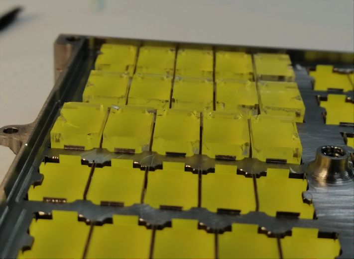
Figure 2. Top: the working principle of a siswich detection system. The SDD, directly facing the sky, is coupled with
a GAGG:Ce scintillator crystal. The low energy radiation (below ∼30 keV) interacts in the SDD. Photons with higher
energy cross the SDD and interact in the scintillator. The light output is collected by SDD. Bottom: efficiency vs. photon
energy for the direct detection in the SDD (black curve) and through light conversion in the GAGG:Ce (Blue curve).

to other scintillator materials largely used in the recent years in space-borne experiments for γ-ray astronomy
(e.g. BGO or CsI).

                         5. THE HERMES SILICON DRIFT DETECTORS
The SDD development builds on the state-of-the-art results achieved within the framework of the Italian ReDSoX
collaboration∗ , with the combined design and manufacturing technology coming by a strong synergy between
INFN-Trieste and Fondazione Bruno Kessler (FBK, Trento), in which both INFN and FBK co-fund the produc-
tion of ReDSoX Silicon sensors. Thanks to several project funded by ASI, INAF and INFN a large amount of
work was done in past years to consolidate the design of SDDs, as well as the production process, for different
applications, for both on-ground and space-based experiments.13–19 The current state of the consolidated de-
sign/process concerns, for example, pitch and distance of the drift cathodes, low power consumption of sensors,
extremely low dark current, high detection efficiency (both for ionizing radiation and optical photons), enhanced
efficiency on the sensor edges, optimized charge collection efficiency. The SDDs are the base elements around
which the overall P/L is designed. The HERMES SDD design is shown in Figure 3. Nominal thickness of the
SDD arrays is 450 µm, with a certified standard deviation of 2.88 µm (by manufacturer). The SDD is orga-
nized in a 2×5 array. Guard rings surrounds the SDD matrix, allowing for a correct electric field termination.
The guard ring area is passive, thus the overall geometric area of the SDD device is 39.6×14.5 mm2 , while the
sensitive area of each SDD cell is 6.05×7.44 mm2 . A single crystal (∼12.1×6.94 mm2 and 15.0 mm thick) is
coupled with two SDD channels on the p-side. On this side to avoid optical cross-talk coming from different
crystals, a metal implant strip 0.5 mm wide is present between adjoining couple of cells (Figure 3 right panel).
With this configuration a signal from a single isolated SDD channel will be considered to be originated by the
   ∗
       http://redsox.iasfbo.inaf.it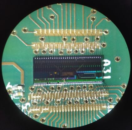
direct absorption of an X-ray in silicon, while a trigger (with comparable amplitude) from the two SDD channels
coupled to the same crystal will be considered as a γ-ray event given the expected uniform illumination on both
SDD cells by the scintillation light.

                                  Figure 3. SDD design. Left: p-side, right: n-side

                             6. THE HERMES READOUT ASIC: LYRA
The potentially high energy resolution of SDDs can be reached only with highly custom and advanced front-end
electronics requiring a preamplifier in close proximity to the anode.20 Being the HERMES detector constituted by
120 channels distributed over a total geometrical area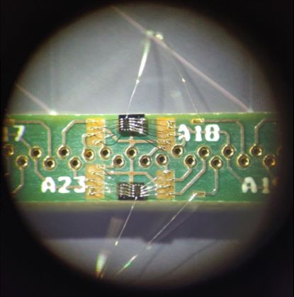
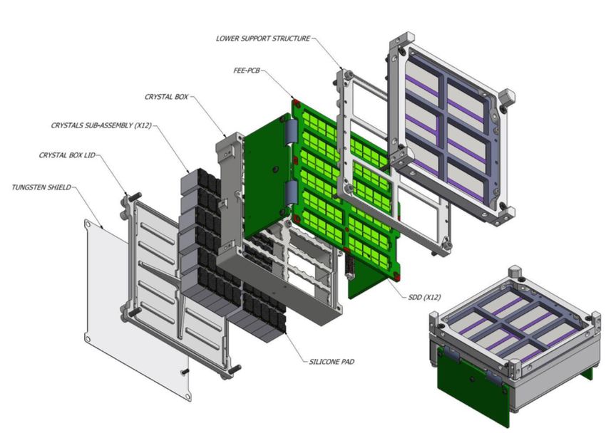
Figure 4. Architecture of the LYRA chipset with 120 LYRA-FE connected to 120 anodes of the SDD and 4 LYRA-BE.

includes a configuration register and an output multiplexer followed by an analog buffer to drive the input load
on-board FPGA. Through the multiplexer all the analog outputs of each SDD (in shaper and in stretcher mode)
can be read-out as well as the event detection triggers. The threshold for the discriminator can be programmed
in two steps through the configuration serial register: a coarse value for all channel and a fine one for each pixel.
For debug purpose all the pixels can be disabled by suitable configuration bits if required.

 Figure 5. Microscope view of the LYRA-FE (left) and LYRA-BE (right) ASICs integrated on the FEE breadboard.
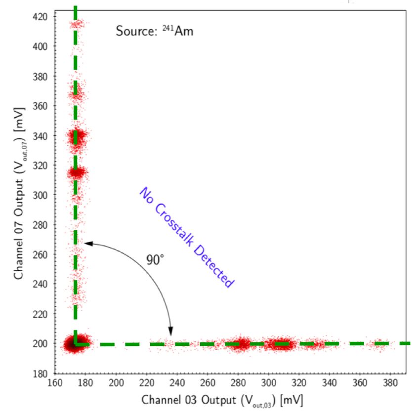
Figure 6. HERMES FEE breadboard (left), measured channel cross-talk (center) and energy spectrum acquired with a
55
   Fe radioisotope (right).

   7. BREADBOARD FOR CROSS-TALK AND PRELIMINARY PERFORMANCE
                         MEASUREMENTS
A FEE breadboard has been designed and manufactured to consolidate the PCB design verifying the system
requirements in terms of performances. The rigid-flex technology used to cope with the strong space constraints
imposed by the S/C, as well as the architecture of the readout electronics with two different ASIC exploiting
current-based interfaces, represent the main innovative points of the final FEE PCB. An electrical characterization
was therefore carried out to verify the absence of channel cross-talk that could degrade the energy resolution
and the event discrimination performance.
    Thanks to the modular design of the HERMES detector, the PCB layout of the test breadboard has been
limited to the routing of a single quadrant (40 LYRA-FE dies) integrating 2 SDD detectors for a total of 20 SDD
cells (Figure 6, left). The channel cross-talk that could be introduced by the reduced distance of PCB traces
carrying the LYRA-FE output analog signals has been characterized in INAF/OAS laboratories, in order to verify
the PCB layout and to confirm current-based interface between the LYRA-FE analog outputs and the LYRA-BE
analog inputs. Central panel of Figure 6 shows the scatter plot of the non-correlated (241 Am radioactive source)
on two channels with adjacent copper traces in the PCB. The absence of systematic correlations of the two
signals (shown as a perfect orthogonality between the signals generated by the two channels) demonstrates the
negligibility of the cross-talk contribution to the system performance. Right panel of Figure 6 shows instead
a 55 Fe spectrum acquired with the integrated breadboard in the INAF/OAS climatic chamber at a detector
temperature of +3 ◦ C. The energy resolution at the 5.9 keV peak is 311 eV FWHM. A detailed description of
simulation and experimental results can be found in.23, 24

   8. THE DEMONSTRATION MODEL: THE FIRST INTEGRATED COMPLETE
                       HERMES DETECTOR
Due to the required readiness level and the reduced development time, in the development plan of HERMES
project the conventional model philosophy was customised, introducing what we called Payload Demonstra-
tion Model (DM). This represent the first completely integrated non-flight HERMES payload, to be dedicated
to validate the integration procedure, and to functional and preliminary performance tests, including verifica-
tion/qualification tests. The DM is described more in detail in other proceedings in this volume.6 The HERMES
payload integration workflow is summarised in the Figure 7, where the whole integrated FEE PCB is shown
on the left, the crystal box with the individual wrapped crystals in the middle and whole integrated Detector
Assembly on the right.
    Although the P/L DM is a non-flight element, it has been integrated with a representative set of flight-like
components, following the finalized AIT/V procedures. The whole integrated Detector Assembly is composed
by:

   • Mechanical assembly;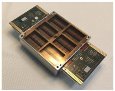
Figure 7. HERMES Detector Assembly workflow. The whole integrated FEE PCB (left) includes 120 LYRA-FEs, 12
SDD matrix and 4 LYRA-BEs; the crystal box (middle) contains 60 wrapped GAGG:Ce crystals, optical pads are also
visible; whole integrated Detector Assembly (right) include a dummy optical filter, which is also visible.

   • Optical filter;
   • FEE board equipped with:
        – 4 LYRA-BE ASICs (one per DA quadrant);
        – 120 LYRA-FE ASICs (30 per quadrant);
        – 12 SDD arrays (4 in-spec + 8 dummy, mechanically representative);
   • 60 GAGG:Ce crystals;
   • Fully representative optical coupling and crystal preload pads;
   • Tungsten shields;

    Because of the mechanical fragility of the quite thin SDDs (450 µm) combined with soft optical coupling pads
between crystals and SDD matrix and the PCB support for Silicon sensor only on the surrounding perimeter, an
additional frame (ABS+Kovar) is glued on the p-side of SDD for mechanical strenghtening. The frame geometry
is also optimised to minimize potential optical cross-talk between contiguous crystals. This frame (white) is
clearly visible in the Figure 7, left. Here the reinforced SDD are glued on the bottom side of FEE PCB (in
the Figure 7 left, the FEE PCB is up side down), facing the frame side towards scintillators. For the optical
coupling a soft silicone pad (one per crystal) is used. To facilitate the coupling of 60 crystals and 12 SDD
matrices, wrapped scintillator crystals are arranged in the so called crystal box (Figure 7, center). This box is
optimised to precisely couple crystals and controlling also the compression against Silicon sensors. Completing
the integration of Detector Assembly is the mechanical structure on the top of FEE PCB, a two-component
frame designed to fix FEE PCB in a ”sandwich” configuration towards the crystal box. The top mechanical
structure is able also to accommodate an optical filter. A dummy optical filter is visible in the Figure 7 right.

    9. DETECTOR ASSEMBLY: PRELIMINARY PERFORMANCE EVALUATION
In order to assess the X-rays and γ-rays detection capabilities and preliminary performance, the integrated
Detector Assembly (DA) has been characterized with radioactive sources at the IAPS Rome facility. The DA has
been powered by means of unfiltered laboratory power supplies connected, through an adapter board, directly
to the LYRA-BE and LYRA-FE ASIC and to the SDD bias network. The LYRA-BE ASICs command and
communication tasks have been managed through a custom Test Equipment including a commercial multi-
channel fast ADC (CAEN DT5740) for data acquisition. The Detector Assembly has been characterized with
X-ray sources at the IAPS laboratories. A series of energy spectra have been acquired at +26 ◦ C and +5 ◦ C by
illuminating the detector with 55 Fe (Mn Kα at 5.9 keV, Mn Kβ at 6.49 keV) and 109 Cd (Ag Kα at 22.1 keV,
Ag Kβ at 24.9 keV). In Figure 8 we show an example of the collected X-ray spectra: on the left a raw spectrum,
i.e. without any selection between X-rays and γ-rays, acquired stimulating the detector simultaneously with 55 Fe
and 109 Cd sources at 26 ◦ C, while on the right panel a 55 Fe spectrum is shown.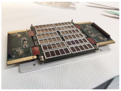
Figure 8. Left: 55 Fe and 109 Cd spectrum acquired on one detector channel at a temperature of (26±1) ◦ C. Right:   55
                                                                                                                         Fe
spectrum acquired at T = 26 ± 1 ◦ C, where the Mn Kα and Mn Kβ best-fit was used to estimate the overall noise.

    The characterization of the integrated DA included the comparison between the leakage current measurement
for all SDD cells and the final noise performances estimated by 55 Fe spectra. Using the Ileak values, measured for
each SDD cell, and the noise values estimated by X-rays spectra, we verified the Ileak -ENC relationship obtained
for the SDD+LYRA system by means of simulations. Figure 9 shows the measured Ileak -ENC values for each
channel (black circles), superimposed to the simulated system performance for the two selectable peaking times
(red and blue areas, τpeak =1.6 µs and 2.3 µs respectively). Although a set-up induced noise excess (∼10 e−
r.m.s) is evident for low detector leakage currents, for Ileak > 90 pA the experimental data match the expected
system performance. Noise performance with a flight-representative set-up will be assessed after the electrical
integration of the power-supply unit (PSU) PCB with the DA. Using the current temporary set-up, an average
value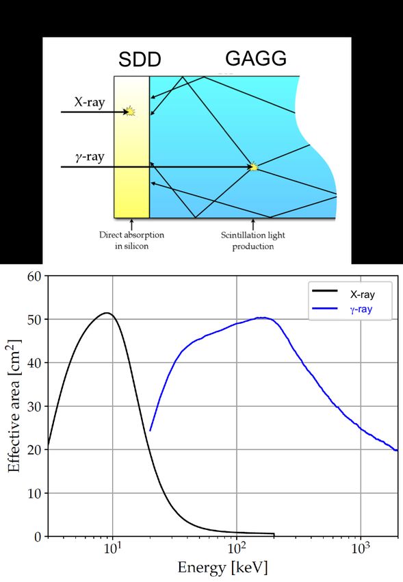
Figure 10. Typical 137 Cs spectrum acquired on a single detector channel at a temperature of T = 26 ± 1 ◦ C, used to
estimate γ-ray detection capabilities and performance.

Review milestone. In this scenario, the experimental measurements described in the previous sections were used
to demonstrate the satisfaction of requirements for both beginning-of-life, corresponding roughly to the measure-
ments at +5 ◦ C, and end-of-life conditions, corresponding to the +26 ◦ C measurements, given the worsening of
performance induced on the silicon sensor due to radiation damage during in-orbit life.
    As an outcome of these activities, the HERMES wide energy range compact detector, sensitive from 2 keV
up to 2 MeV, is now ready for all the necessary forthcoming steps of the System Assembly, Integration and Test
of its Flight versions, in the Phase D of the project.

                                         ACKNOWLEDGMENTS
This project has received funding from the European Union Horizon 2020 Research and Innovation Framework
Programme under grant agreement HERMES-Scientific Pathfinder n. 821896 and from ASI-INAF Accordo
Attuativo HERMES Technologic Pathfinder n. 2018-10-HH.0.

                                               REFERENCES
 [1] Fuschino, F., Campana, R., Labanti, C., Evangelista, Y., Feroci, M., Burderi, L., Fiore, F., Ambrosino,
     F., Baldazzi, G., Bellutti, P., Bertacin, R., Bertuccio, G., Borghi, G., Cirrincione, D., Cauz, D., Ficorella,
     F., Fiorini, M., Gandola, M., Grassi, M., Guzman, A., Rosa, G. L., Lavagna, M., Lunghi, P., Malcovati,
     P., Morgante, G., Negri, B., Pauletta, G., Piazzolla, R., Picciotto, A., Pirrotta, S., Pliego-Caballero, S.,
     Puccetti, S., Rachevski, A., Rashevskaya, I., Rignanese, L., Salatti, M., Santangelo, A., Silvestrini, S.,
     Sottile, G., Tenzer, C., Vacchi, A., Zampa, G., Zampa, N., and Zorzi, N., “HERMES: An ultra-wide band X
     and gamma-ray transient monitor on board a nano-satellite constellation,” Nuclear Instruments and Methods
     in Physics Research A 936, 199–203 (Aug. 2019).
 [2] Sanna, A. et al., “Timing techniques applied to distributed modular high-energy astronomy: the
     H.E.R.M.E.S. project,” Society of Photo-Optical Instrumentation Engineers (SPIE) Conference Se-
     ries, 11444-251 (2020).
 [3] Fiore, F. et al., “The HERMES-Technologic and Scientific Pathfinder,” Society of Photo-Optical Instrumen-
     tation Engineers (SPIE) Conference Series, 11444-166 (2020).
 [4] Colagrossi, A., Prinetto, J., Silvestrini, S., and Lavagna, M. R., “Sky visibility analysis for astrophysical
     data return maximization in HERMES constellation,” Journal of Astronomical Telescopes, Instruments,
     and Systems 6(4), 1 – 25 (2020).
[5] Gatti, E. and Rehak, P., “Semiconductor drift chamber - an application of a novel charge transport scheme,”
Nuclear Instruments and Methods in Physics Research 225(3), 608 – 614 (1984).
[6] Evangelista, Y. et al., “The scientific payload on-board the HERMES-TP and HERMES-SP CubeSat mis-
sions,,” Society of Photo-Optical Instrumentation Engineers (SPIE) Conference Series, 11444-168 (2020).
[7] Marisaldi, M., Labanti, C., and Soltau, H., “A pulse shape discrimination gamma-ray detector based on a
silicon drift chamber coupled to a CsI(Tl) scintillator: prospects for a 1 keV-1 MeV monolithic detector,”
IEEE Transactions on Nuclear Science 51(4), 1916–1922 (2004).
[8] Marisaldi, M., Labanti, C., Fuschino, F., and Amati, L., “A broad energy range wide field monitor for next
generation gamma-ray burst experiments,” Nuclear Instruments and Methods in Physics Research Section
A: Accelerators, Spectrometers, Detectors and Associated Equipment 588(1), 37 – 40 (2008). Proceedings
of the First International Conference on Astroparticle Physics.
[9] Kamada, K., Yanagida, T., Pejchal, J., Nikl, M., Endo, T., Tsutsumi, K., Fujimoto, Y., Fukabori, A., and
Yoshikawa, A., “Crystal Growth and Scintillation Properties of Ce Doped Gd3 (Ga, Al)5 O12 Single Crystals,”
IEEE Transactions on Nuclear Science 59(5), 2112–2115 (2012).
[10] Dilillo, G. et al., “A summary on an investigation of GAGG:Ce afterglow emission in the context of future
space applications within the HERMES nanosatellite mission,” Society of Photo-Optical Instrumentation
Engineers (SPIE) Conference Series, 11444-185 (2020).
[11] Ripa, J. et al., “A comparison of trapped particle models in Low Earth Orbit,” Society of Photo-Optical
Instrumentation Engineers (SPIE) Conference Series, 11444-74 (2020).
[12] Campana, R. et al., “The HERMES background and response simulations,” Society of Photo-Optical In-
strumentation Engineers (SPIE) Conference Series, 11444-248 (2020).
[13] Zampa, G., Campana, R., Feroci, M., Vacchi, A., Bonvicini, V., Del Monte, E., Evangelista, Y., Fuschino,
F., Labanti, C., Marisaldi, M., Muleri, F., Pacciani, L., Rapisarda, M., Rashevsky, A., Rubini, A., Soffitta,
P., Zampa, N., Baldazzi, G., Costa, E., Donnarumma, I., Grassi, M., Lazzarotto, F., Malcovati, P., Mas-
tropietro, M., Morelli, E., and Picolli, L., “Room-temperature spectroscopic performance of a very-large
area silicon drift detector,” Nuclear Instruments and Methods in Physics Research Section A: Accelerators,
Spectrometers, Detectors and Associated Equipment 633(1), 15 – 21 (2011).
[14] Campana, R., Zampa, G., Feroci, M., Vacchi, A., Bonvicini, V., Del Monte, E., Evangelista, Y., Fuschino,
F., Labanti, C., Marisaldi, M., Muleri, F., Pacciani, L., Rapisarda, M., Rashevsky, A., Rubini, A., Soffitta,
P., Zampa, N., Baldazzi, G., Costa, E., Donnarumma, I., Grassi, M., Lazzarotto, F., Malcovati, P., Mas-
tropietro, M., Morelli, E., and Picolli, L., “Imaging performance of a large-area silicon drift detector for x-ray
astronomy,” Nuclear Instruments and Methods in Physics Research Section A: Accelerators, Spectrometers,
Detectors and Associated Equipment 633(1), 22 – 30 (2011).
[15] Rachevski, A., Zampa, G., Zampa, N., Campana, R., Evangelista, Y., Giacomini, G., Picciotto, A., Bellutti,
P., Feroci, M., Labanti, C., Piemonte, C., and Vacchi, A., “Large-area linear silicon drift detector design for
x-ray experiments,” Journal of Instrumentation 9, P07014–P07014 (jul 2014).
[16] Campana, R., Fuschino, F., Labanti, C., Marisaldi, M., Amati, L., Fiorini, M., Uslenghi, M., Baldazzi,
G., Bellutti, P., Evangelista, Y., Elmi, I., Feroci, M., Ficorella, F., Frontera, F., Picciotto, A., Piemonte,
C., Rachevski, A., Rashevskaya, I., Rignanese, L. P., Vacchi, A., Zampa, G., Zampa, N., and Zorzi, N.,
“A compact and modular x- and gamma-ray detector with a CsI scintillator and double-readout Silicon
Drift Detectors,” in [Space Telescopes and Instrumentation 2016: Ultraviolet to Gamma Ray ], den Herder,
J.-W. A., Takahashi, T., and Bautz, M., eds., 9905, 1900 – 1909, International Society for Optics and
Photonics, SPIE (2016).
[17] Fuschino, F., Labanti, C., Campana, R., Gangemi, G. C., Marisaldi, M., Rignanese, L. P., Baldazzi, G.,
Elmi, I., Evangelista, Y., Feroci, M., Zampa, G., Zampa, N., Rashevsky, A., Vacchi, A., Rashevskaya, I.,
Fabiani, S., Zorzi, N., Piemonte, C., Bellutti, P., Ficorella, F., Borghi, G., and Burderi, L., “Characterization
of a LaBr3 scintillator with multi-cell Silicon Drift Detector (SDD) readout,” in [Space Telescopes and
Instrumentation 2016: Ultraviolet to Gamma Ray ], den Herder, J.-W. A., Takahashi, T., and Bautz, M.,
eds., 9905, 1910 – 1918, International Society for Optics and Photonics, SPIE (2016).[18] Evangelista, Y., Ambrosino, F., Feroci, M., Bellutti, P., Bertuccio, G., Borghi, G., Campana, R., Caselle, M.,
Cirrincione, D., Ficorella, F., Fiorini, M., Fuschino, F., Gandola, M., Grassi, M., Labanti, C., Malcovati,
P., Mele, F., Morbidini, A., Picciotto, A., Rachevski, A., Rashevskaya, I., Sammartini, M., Zampa, G.,
Zampa, N., Zorzi, N., and Vacchi, A., “Characterization of a novel pixelated silicon drift detector (PixDD)
for high-throughput x-ray astrophysics,” Journal of Instrumentation 13, P09011–P09011 (sep 2018).
[19] Cirrincione, D., Ahangarianabhari, M., Ambrosino, F., Bajnati, I., Bellutti, P., Bertuccio, G., Borghi, G.,
Bufon, J., Cautero, G., Ceraudo, F., Evangelista, Y., Fabiani, S., Feroci, M., Ficorella, F., Gandola, M.,
Mele, F., Orzan, G., Picciotto, A., Sammartini, M., Rachevski, A., Rashevskaya, I., Schillani, S., Zampa,
G., Zampa, N., Zorzi, N., and Vacchi, A., “High precision mapping of single-pixel silicon drift detector
for applications in astrophysics and advanced light source,” Nuclear Instruments and Methods in Physics
Research Section A: Accelerators, Spectrometers, Detectors and Associated Equipment 936, 239 – 241 (2019).
Frontier Detectors for Frontier Physics: 14th Pisa Meeting on Advanced Detectors.
[20] Bertuccio, G., Ahangarianabhari, M., Graziani, C., Macera, D., Shi, Y., Rachevski, A., Rashevskaya, I.,
Vacchi, A., Zampa, G., Zampa, N., Bellutti, P., Giacomini, G., Picciotto, A., and Piemonte, C., “A silicon
drift detector-CMOS front-end system for high resolution x-ray spectroscopy up to room temperature,”
Journal of Instrumentation 10, P01002–P01002 (jan 2015).
[21] Ahangarianabhari, M., Macera, D., Bertuccio, G., Malcovati, P., and Grassi, M., “Vega: A low-power front-
end asic for large area multi-linear x-ray silicon drift detectors: Design and experimental characterization,”
Nuclear Instruments and Methods in Physics Research Section A: Accelerators, Spectrometers, Detectors
and Associated Equipment 770, 155 – 163 (2015).
[22] Campana, R., Evangelista, Y., Fuschino, F., Ahangarianabhari, M., Macera, D., Bertuccio, G., Grassi, M.,
Labanti, C., Marisaldi, M., Malcovati, P., Rachevski, A., Zampa, G., Zampa, N., Andreani, L., Baldazzi, G.,
Monte, E. D., Favre, Y., Feroci, M., Muleri, F., Rashevskaya, I., Vacchi, A., Ficorella, F., Giacomini, G.,
Picciotto, A., and Zuffa, M., “Characterization of the VEGA ASIC coupled to large area position-sensitive
silicon drift detectors,” Journal of Instrumentation 9, P08008–P08008 (aug 2014).
[23] Gandola, M., Grassi, M., Mele, F., Malcovati, P., and Bertuccio, G., “LYRA: A Multi-Chip ASIC Designed
for HERMES X and Gamma Ray Detector,” in [2019 IEEE Nuclear Science Symposium and Medical Imaging
Conference (NSS/MIC) ], 1–3, IEEE (2019).
[24] Grassi, M., Gandola, M., Mele, F., Bertuccio, G., Malcovati, P., Fuschino, F., Campana, R., Labanti, C.,
Fiorini, M., Evangelista, Y., et al., “X-/γ-Ray Detection Instrument for the HERMES Nano-Satellites Based
on SDDs Read-Out by the LYRA Mixed-Signal ASIC Chipset,” in [2020 IEEE International Instrumentation
and Measurement Technology Conference (I2MTC) ], 1–6, IEEE (2020).You can also read