SPECTROSCOPIC EVIDENCE ON REALIZATION OF A GENUINE TOPOLOGICAL NODAL LINE SEMIMETAL IN LASBTE
←
→
Page content transcription
If your browser does not render page correctly, please read the page content below
Spectroscopic Evidence on Realization of a Genuine Topological
                                                                                             Nodal Line Semimetal in LaSbTe

                                                              Yang Wang1,2] , Yuting Qian1,2] , Meng Yang1,2.3] , Hongxiang Chen1,4] ,
                                                              Cong Li1,2] , Zhiyun Tan5 , Yongqing Cai1,2 , Wenjuan Zhao1,2 , Shunye
                                                            Gao1,2 , Ya Feng6 , Shiv Kumar7 , Eike F. Schwier7,8 , Lin Zhao1 , Hongming
arXiv:2102.13324v1 [cond-mat.mtrl-sci] 26 Feb 2021

                                                        Weng1,2,9,10 , Youguo Shi1,2,3 , Gang Wang1,2,9 , Youting Song1 , Yaobo Huang11 ,
                                                              Kenya Shimada7 , Zuyan Xu12 , X. J. Zhou1,2,6,9∗ and Guodong Liu1,9∗
                                                                          1
                                                                              Beijing National Laboratory for Condensed Matter Physics,
                                                            Institute of Physics, Chinese Academy of Sciences, Beijing 100190, China
                                                              2
                                                                  University of Chinese Academy of Sciences, Beijing 100049, China
                                                                      3
                                                                          Center of Materials Science and Optoelectronics Engineering,
                                                               University of Chinese Academy of Sciences, Beijing 100049, China
                                                                                         4
                                                                                             School of Materials Science and Engineering,
                                                                               Fujian University of Technology, Fuzhou 350118, China
                                                                                             5
                                                                                                 School of Physics and Electronic Science,
                                                                                          Zunyi Normal College, Zunyi 563006, China
                                                        6
                                                            Beijing Academy of Quantum Information Sciences, Beijing 100193, China
                                                                  7
                                                                      Hiroshima Synchrotron Radiation Center, Hiroshima University,
                                                                                        Higashi-Hiroshima, Hiroshima 739-0046, Japan
                                                                                    8
                                                                                        Experimentelle Physik VII, Universität Würzburg,
                                                                                        Am Hubland, D-97074 Würzburg, Germany, EU
                                                                    9
                                                                        Songshan Lake Materials Laboratory, Dongguan 523808, China
                                                               10
                                                                    CAS Center for Excellence in Topological Quantum Computation,
                                                                  University of Chinese Academy of Science, Beijing 100190, China
                                                                                             11
                                                                                                  Shanghai Synchrotron Radiation Facility,
                                                                                                  Shanghai Advanced Research Institute,
                                                                               Chinese Academy of Sciences, Shanghai 201204, China
                                                                                        12
                                                                                             Technical Institute of Physics and Chemistry,
                                                                                Chinese Academy of Sciences, Beijing 100190, China
                                                                                ]
                                                                                    These people contributed equally to the present work.

                                                                                                                   1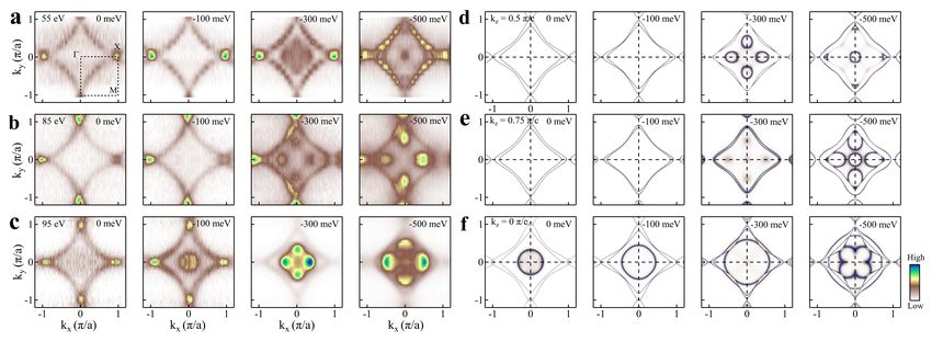
∗
           Corresponding authors: XJZhou@iphy.ac.cn and gdliu ARPES@iphy.ac.cn
                                   (Dated: February. 22, 2021)

                                            Abstract
  The nodal line semimetals have attracted much attention due to their unique topological elec-
tronic structure and exotic physical properties. A genuine nodal line semimetal is qualified by the
presence of Dirac nodes along a line in the momentum space that are protected against the spin-
orbit coupling. In addition, it requires that the Dirac points lie close to the Fermi level allowing
to dictate the macroscopic physical properties. Although the material realization of nodal line
semimetals have been theoretically predicted in numerous compounds, only a few of them have
been experimentally verified and the realization of a genuine nodal line semimetal is particularly
rare. Here we report the realization of a genuine nodal line semimetal in LaSbTe. We investigated
the electronic structure of LaSbTe by band structure calculations and angle-resolved photoemission
(ARPES) measurements. Taking spin-orbit coupling into account, our band structure calculations
predict that a nodal line is formed in the boundary surface of the Brillouin zone which is robust and
lies close to the Fermi level. The Dirac nodes along the X-R line in momentum space are directly
observed in our ARPES measurements and the energies of these Dirac nodes are all close to the
Fermi level. These results constitute clear evidence that LaSbTe is a genuine nodal line semimetal,
providing a new platform to explore for novel phenomena and possible applications associated with
the nodal line semimetals.

                                                2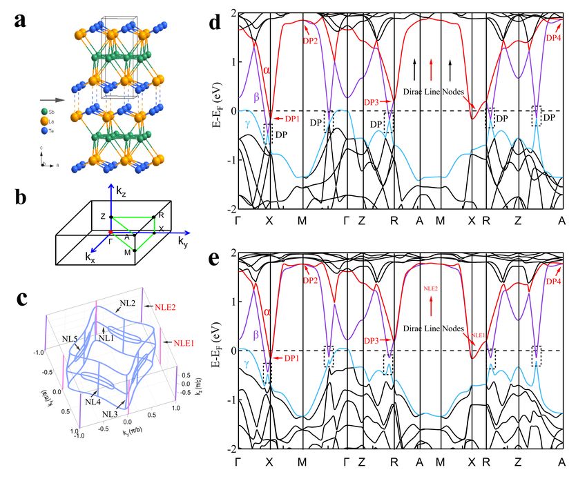
Stimulated by the discovery of topological insulators [1–7], searching for new types of
topological materials with novel quantum states has become one of the central topics in
current condensed-matter physics [8–14]. Recently, topological semimetals have attracted
intensive interest for their exotic physical properties and potential applications [15–21].
The band crossings of a topological semimetal can be categorized by their dimensions in
momentum space: the zero-dimensional nodal point [22–24], one-dimensional nodal line
[25, 26], and two-dimensional nodal surface [27–29]. For the first case, when two or more
bands cross each other at a discrete point in Brillouin zone (BZ), it can form Dirac point
[15, 17, 22, 23, 30], Weyl point [24, 31–37], threefold [38–40] or even multifold nodal point
[41]. Different from nodal points, one-dimensional nodal curve can take various shapes such
as a nodal line, a nodal ring forming a closed loop, or a nodal chain consisting of several
inter-connected loops [26]. The material realization of the nodal line semimetals have been
theoretically predicted in many compounds [25, 42–45], but only a few of them have been
experimentally examined by angle-resolved photoemission spectroscopy (ARPES) such as
PtSn4 [46], CaAgX (X=P, As) [47–49], Ta3 SiTe6 [50], monolayer Cu2 Si [51], XB2 (X=Zr,
Ti, Al, Mg) [52–56], RAs3 (R=Ca,Sr) [57, 58], Pt2 HgSe3 [59], Co2 MnGa [60], ZrSiS family
[61–73], single-layer GdAg2 [74], InBi [75], PbTaSe2 [76], IrO2 [77] and RuO2 [78].
  Strictly speaking, two requirements are necessary for realizing a genuine nodal line
semimetal. One is the presence of Dirac nodes along a line and the nodes retain gap-
less under the spin-orbit coupling (SOC). The other is that the Dirac points should lie close
to the Fermi level allowing to produce exotic physical phenomena. Many of the nodal line
semimetals proposed without considering SOC may not fall into the category because the
Dirac points become unstable and get gapped when SOC is considered, as seen in CaAgX
(X=P, As) [47–49], Ta3 SiTe6 [50], monolayer Cu2 Si [51], XB2 (X=Zr, Ti, Al, Mg )[52–56],
RAs3 (R=Ca, Sr) [57, 58], Pt2 HgSe3 [59] and Co2 MnGa [60]. The genuine topological nodal
line semimetals that have been proposed and can satisfy the two criteria are rare [77, 78].
The layered ternary WHM system (W represents transition metal Zr, Hf, or rare earth el-
ement La, Ce, Gd; H represents group IV or group V element Si, Ge, Sn, or Sb, and M
represents group VI element O, S, Se, and Te) [79] has become an important candidate
family of topological nodal line semimetals. Without SOC or when the SOC is negligible,
this system can host nodal lines and nodal surface, which have been confirmed experimen-
tally by ARPES measurements in HfSiS [61], ZrSiX (X=S, Se, Te) [62–66], ZrGeTe [67, 68]

                                            3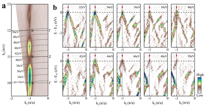
and GdSbTe [69]. When the SOC is taken into account, however, most of the nodal lines
and nodal surface become gapped, leaving only two topological nodal lines in the bound-
ary surface of Brillouin zone [71, 72]. Meanwhile, the robust nodal lines observed so far in
this system stay away from the Fermi level, contributing little to the macroscopic physical
properties. Finding genuine topological nodal line semimetals is essential for exploring new
phenomena and realizing exotic properties.
  In this paper, we report identification of LaSbTe as a genuine topological nodal line
semimetal. Compared to the ZrSiS system in which the robust Dirac nodal lines exist
at the Brillouin zone boundary but their energy position stays away from the Fermi level
(∼0.6 eV below the Fermi level in ZrSiS and HfSiS[71]), LaSbTe possesses not only the
robust nodal lines but also these nodal lines locate right near the Fermi level so that the
exotic topological properties may manifest. We carried out band structure calculations and
ARPES measurements to investigate the topological electronic structure of LaSbTe. Our
band structure calculations combined with symmetry analyses indicate that two nodal lines
along X-R and M-A lines in momentum space can be formed and stay robust after the SOC
is considered. Among these two nodal lines, the one along the X-R direction lies close to
the Fermi level while the other one along M-A direction stays far from the Fermi level. Our
ARPES measured results are in good agreements with the band structure calculations. In
particular, we clearly observed Dirac nodes along the X-R line with the Dirac points close to
the Fermi level. These results provide clear evidence that LaSbTe is a genuine topological
nodal line semimetal.
  High-quality single crystals of LaSbTe were synthesized by flux method. The samples are
characterized by single crystal X-ray diffraction measurements. Single crystal X-ray diffrac-
tion measurement was conducted on Bruker D8 high resolution four-circle diffractometer at
273 K using Mo Kα radiation (λ=0.71073 Å), indicating that our LaSbTe samples crystallize
in a nonsymmorphic space group P 4/nmm (no.129) with PbFCl-type tetragonal structure:
a=b=4.399 Å and c=9.566 Å. The measured crystal parameters of LaSbTe are summa-
rized in Table I-III in Supplementary Materials[80]. This structure is identical to the WHM
family. The Sb atoms constitute a two-dimensional square net sandwiched in between two
LaTe layers (Fig. 1a). ARPES measurements were performed at Hiroshima Synchrotron
Radiation (HiSOR) BL-1 Beamline [81, 82], the ‘Dreamline’ Beamline of the Shanghai Syn-
chrotron Radiation Facility (SSRF) and the ARPES system in our lab [83, 84]. The energy

                                             4
resolution is ∼30 meV and the angular resolution is ∼0.3 degree. In order to get complete
electron structure, two polarization geometries were used in our ARPES measurements. In
one polarization geometry (LV), the electric field vector of the incident light is perpendicular
to the horizontal plane, while in the other polarization geometry (LH), it lies within the hor-
izontal plane. All the samples were cleaved in situ and measured at different photon energies
in ultrahigh vacuum with a base pressure better than 5.0×10⁻¹¹ mbar. The first-principles
band-structure calculations based on the density functional theory (DFT) have been done
using the Vienna ab initio simulation package (VASP) [85] within the generalized gradient
approximation (GGA) of Perdew-Burke-Ernzerhof type [86]. We take 300 eV as the cut-off
energy for plane wave expansion. The 8 × 8 × 4 k-mesh is used as grids of Brillouin zone
(BZ) in the self-consistent process. The relaxed lattice parameters a=b=4.421 Å, c=9.659
Å are employed. The Wannier90 [87] and WannierTools [88] are used to calculate the Fermi
surface and find nodes based on the maximally localized Wannier functions which consist of
p orbits of Sb and Te, and d orbits of La.
We start our discussion with bulk electronic structure calculations of LaSbTe. Symmetries
are crucial to understand the electronic structure of materials as they protect the band
crossings in the Brillouin zone in high-symmetry planes, lines or points[26, 29]. For the
tetragonal LaSbTe crystallized in nonsymmorphic space group P 4/nmm, the glide mirror
n o n o n o n o
M̃z = Mz | 12 21 0 , the mirror M̃x = Mx | 12 00 , M̃y = My |0 21 0 , M̃xy = Mxy | 21 12 0 ,
n o
the spacial inversion {P|000} symmetries and the two screw symmetries: C˜2x = C2x | 12 00
n o
and C˜2y = C2y |0 1 0 are especially important. Combining with time-reversal symmetry T ,
2
these symmetries can lead to nonsymmorphically enforced degeneracy at the boundary of
Brillouin zone that give rise to multiple nodal lines. To clarify the topology of electronic
structure of LaSbTe protected by different symmetries, we calculated the Dirac nodal lines
in three-dimensional (3D) Brillouin zone (Fig. 1c) and the band structures of bulk LaSbTe
without (Fig. 1d) and with SOC (Fig. 1e). Because the bands close to the Fermi level are
mainly dominated by the α, β and γ in Fig. 1d and Fig. 1e, we will focus on the nodal lines
formed by these three bands.
Figure 1c shows the schematic of the calculated nodal line configurations formed by β-γ
band (NL1-NL5) in the absence of SOC and by α-β band (NLE1 and NLE2) in the presence
of SOC in 3D Brillouin zone. They represent the locations of all the Dirac nodes in three-
5dimensional momentum space formed from α, β and γ bands although the energy of the
Dirac nodes can be different. The nodal lines formed by β-γ band can take various shapes
under different symmetry protections as shown by the light blue curves in Fig. 1c. They
all lie inside the first Brillouin zone. We can find two diamond-shaped nodal lines: NL1 in
kz =0 plane and NL2 in kz =π plane that are protected by the glide mirror symmetry M̃z . In
addition, there are two vertical nodal lines, NL3 protected by M̃x and NL4 by M̃xy . These
nodal lines form a 3D cage-like structure. They are 2-fold degenerate and not stable in the
presence of SOC which will open a gap at the Dirac point.
The band crossings formed by α-β band form two nodal surfaces in the kx =π and ky =π
planes due to the combined symmetry C˜2y T as reported in WHM family [66, 89]. When SOC
is taken into consideration, all band crossings are gapped except for the two lines along R-X
and A-M directions and some one-dimensional curves at generic k points in A-M-X-R-A plane
owing to accidental degeneracy that are far away from Fermi level and will not be considered
further. The nodal lines along R-X and A-M high symmetry directions, as labeled by NLE1
and NLE2 in Fig. 1c, host robust 4-fold degenerate massless Dirac nodal lines protected
by nonsymmorphic symmetry at the boundary of Brillouin zone [26, 64, 71, 90, 91] and
can be understood in the following way. Firstly, in the spinful case, it is well known that
there exists Kramers’ pair due to (PT )2 =-1. Secondly, the two high symmetry lines R-
X and A-M have higher symmetry than other points on the ky =π plane such that bands
along these two lines are at least doubly degenerate (|ψ1 i, |ψ2 i) protected by M̃y . Thirdly,
since the M̃y is a nonsymmorphic symmetry, anti-commutation relation {PT , M̃y }=0 is
satisfied. Considering the above three conditions, there must exist a 4-fold degenerate
state (|ψ1 i, PT |ψ1 i, |ψ2 i, PT |ψ2 i) where each Kramers’ pair (|ψ1,2 i, PT |ψ1,2 i) belongs to
two orthogonal states with the same M̃y eigenvalues [26, 91]. Therefore, the NLE1 and
NLE2 are symmetry enforced and appear along high symmetry lines at the boundary of
Brillouin zone.
The formation of nodal lines in LaSbTe can be seen directly from the calculated band
structures which show the overall α, β and γ bands, derived mainly from the Sb px and py
orbits, in the entire 3D Brillouin zone. Without considering SOC, the location of the Dirac
points or nodal lines formed from α-β band (red arrows) and β-γ band (dashed black boxes)
are marked in Fig. 1d. When SOC is taken into consideration as shown in Fig. 1e, all the
Dirac points formed by β-γ band are gapped. But some Dirac points formed by α-β band
6remain intact. The SOC causes the band splitting along M-X (A-R) direction and turns the
initial Dirac line nodes (marked by black arrows in Fig. 1d) into topologically trivial 2-fold
spin-degenerate bands. However, the two Dirac lines along the R-X and A-M lines survive
under the protection of nonsymmorphic symmetry, as labeled by red arrows in Fig. 1e. The
NLE2 nodal line lies about 1.6 eV above the Fermi level while the NLE1 nodal line lies right
at the Fermi level. These calculation results indicate that LaSbTe is a genuine nodal line
semimetal.
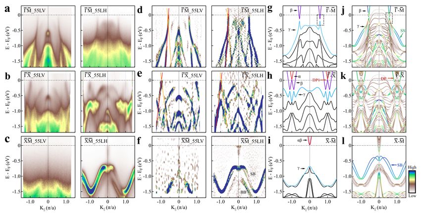
Now we come to the electronic structure of LaSbTe from our ARPES measurements. Fig.
2a-2c show the Fermi surface mapping and constant energy contours of LaSbTe measured
with photon energies of 55 eV (Fig. 2a), 85 eV (Fig. 2b) and 95 eV (Fig. 2c). We can
clearly see a large diamond-shaped Fermi surface centered around Γ̄ point. We also observe
strong spectral weight at the X̄ points. For different photon energies, the evolution of
constant energy contours with binding energy is markedly different for the three different
photon energies. Fig. 2d-2f show the calculated Fermi surface and constant energy contours
of LaSbTe at kz planes of 0.5 π/c (Fig. 2d), 0.75 π/c (Fig. 2e) and 0 π/c (Fig. 2f),
corresponding to the photon energy of 55 eV, 85 eV and 95 eV, respectively. The diamond-
shaped Fermi surface originates from β band and the feature around X̄ point is mainly from
the Dirac-like band formed from α or β bands, as shown in Fig. 1e. The measured results
show an overall agreements with the band structure calculations in terms of the observation
of a large diamond-shaped Fermi surface and the feature at the X̄ points.
Figure 3 shows the band structure of LaSbTe measured along three high symmetry di-
rections under different polarization geometries (more data measured at different photon
energies can be found in Supplementary Fig. S2 and Fig. S3[80]). We find that the observed
band structures measured under different polarizations are quite different due to photoemis-
sion matrix element effect. Therefore, our measurements under two distinct polarizations
are helpful to directly reveal the band structure depending on the orbital symmetry with
respect to the detection plane. To better identify the band structure, we also take second
derivative images (Fig. 3d-3f) of the original data (Fig. 3a-3c). For comparison, we put
the corresponding calculated bulk band in Fig. 3g-3i and carried out slab calculations (Fig.
3j-3l) that can handle surface states.
For the band structure along Γ̄-M̄ direction, a linearly dispersive band crosses the Fermi
level as shown in Fig. 3d marked by red and orange lines, which gives rise to the diamond-
7shaped Fermi surface. This band can extend to a high binding energy of ∼2 eV. It has
−1
a very high Fermi velocity of ∼12 eV·Å that is larger than those found in some typical
−1 −1
Dirac materials like graphene (6.7 eV·Å ) [92] , SrMnBi2 (10.6 eV·Å ) [93] and ZrSiS (4.3
−1
eV·Å ) [64]. The measured band structures (Fig. 3d) areconsistent with the calculated
bands (Fig. 3g) in terms of both the number and the position of the bands. For the band
structure along Γ̄-X̄ direction, a Dirac like band is observed crossing the Fermi level as shown
in Fig. 3e marked by red and orange lines. The Dirac point lies exactly at X̄ point and
its energy position is rather close to the Fermi level. Again, the measured band structures
(Fig. 3e) are consistent with the calculation (Fig. 3h) in terms of the number, shape and
the position of the bands. For the band structure along M̄ -X̄ direction, a tiny electron-like
band is observed that crosses the Fermi level at the X̄ point as shown in Fig. 3f. In addition,
two groups of bands are observed, labeled as SB and BB in Fig. 3f. Each group of band
is further composed of two bands. These results are well reproduced in the band structure
calculations (Fig. 3i and 3l), which indicate that the SB bands represent surface states
while the BB bands are bulk states. The SB band exhibits little change when measured at
different photon energies (Fig. S3 in Supplementary materials[80]), further confirming its
surface state nature.
It is noted that we only observed single sheet of the diamond-shaped Fermi surface, even
at different binding energies (Fig. 2a-2c). According to the band structure calculations, two
sheets of the Fermi surface are expected (Fig. 2d-2f). We also only observed a single band
over a large energy range (∼0.6 eV) near the Fermi level measured along Γ̄-M̄ direction (Fig.
3a and Fig. 3d) although two linear bands are expected in this energy range from the band
calculations (Fig. 1d and Fig. 1e). Most of the ARPES measurements on WHM system have
observed double sheets Fermi surface [61, 62, 65, 66, 68, 70, 71]. A single sheet Fermi surface
has also been reported before in GdSbTe but the origin is unclear [69]. By carefully examing
the measured band structures in Fig. 3d, we believe this is caused by the photoemission
matrix element effect. As seen in the right panel of Fig. 3d, in this particular polarization
geometry, the two linear bands can actually be observed at high binding energy between
1.0∼1.5 eV although the right-side band is weaker than the left-side one. When moving to
lower binding energy between 0∼1.0 eV, the right-side band gets strongly suppressed while
the left-side one remains strong and becomes dominant. When the sample is measured in
another polarization geometry (left panel of Fig. 3d), the right-side band is fully suppressed.
8The spectral weight suppression of the right-side linear band results in our observation of
single sheet diamond-like Fermi surface and a single band near the Fermi level.
From the band structure calculations, the Dirac nodes along the diamond-shaped Fermi
surface are gapped when the SOC is considered (Fig. 1d and 1e). The calculated gap size
is about 40 meV. To check on the gap opening, we carefully examined the band structures
measured along Γ̄-M̄ direction using different photon energies (Fig. S2 in Supplementary
materials[80]). We observed sharp single band over an energy range of 0∼0.6 eV below the
Fermi level. There is a finite spectral intensity at the Fermi level and the band intensity
shows a smooth variation with the binding energy (Fig. S2i-S2l). We do not observe clear
signatures of gap opening along the Γ̄-M̄ direction. This is probably because the gap opening
induced by SOC is small that exceeds our present detection limit.
As predicted by band structure calculations, LaSbTe is a nodal line semimetal because
of the presence of the nodal line along X-R direcion that is robust against the SOC and lies
close to the Fermi level. To examine on the band structure along kz direction, we carried
out measurements along Γ̄-X̄ direction with different photon energies between 26 eV and 95
eV. Fig. 4a shows the Fermi surface mapping in Γ-X-R-Z-Γ plane of LaSbTe crossing the X̄
point along Γ̄-X̄ direction. A one-dimensional linear Fermi surface is clearly observed along
the X-R momentum line. Fig. 4b displays representative band structures measured using
different photon energies between 32 eV and 50 eV, that corresponds to a full kz period.
Dirac-like structure can be observed in all the measurements using different photon energies
as marked by the red arrows in Fig. 4b. The Dirac cones lie at the X̄ point along the X-R
line in momentum space and their energies are all close to the Fermi level. These results
strongly indicate that there is a nodal line formed along the X-R direction.
In summary, by carrying out ARPES measurements combined with band structure
calculations, we have systematically investigated the electronic structures of LaSbTe. Our
band structure calculations predict the formation of five nodal lines derived from the β-γ
band including two diamond-like nodal lines, and two nodal surfaces (kx =π and ky =π
plane) from the α-β band without considering SOC. Taking SOC into account, band
calculations indicate that those five nodal lines from β-γ band become unstable and are
gapped at the Dirac points while the two nodal lines from α-β band are robust. Among
these two nodal lines, the one along M-A direction stays far away from Fermi level while
the other one along X-R direction lies close to the Fermi level. Our ARPES results are in
9good agreements with the band structure calculations. We observed a diamond-like Fermi
surface. In particular, we directly observed Dirac nodes along the X-R direction with their
energy position close to the Fermi level. These results provide strong evidence that LaSbTe
is a genuine topological nodal line semimetal, which is the first case that is realized in
the WHM family. This finding will facilitate to explore for novel phenomena and possible
applications associated with the nodal line semimetals.
[1] M. Z. Hasan, and C. L. Kane, Topological insulators. Rev. Mod. Phys. 82, 3045 (2010).
[2] X. L. Qi, and S. C. Zhang, Topological insulators and superconductors. Rev. Mod. Phys. 83,
1057 (2011).
[3] L. Fu, and C. L. Kane, Topological insulators with inversion symmetry. Phys. Rev. B 76,
045302 (2007).
[4] D. Hsieh, D. Qian, L. Wray, Y. Xia, Y. S. Hor, R. J. Cava, and M. Z. Hasan, A topological
Dirac insulator in a quantum spin Hall phase. Nature 452, 970 (2008).
[5] H. Zhang, C. X. Liu, X. L. Qi, X. Dai, Z. Fang, and S. C. Zhang, Topological insulators in
Bi2 Se3 , Bi2 Te3 and Sb2 Te3 with a single Dirac cone on the surface. Nat. Phys. 5, 438 (2009).
[6] Y. L. Chen, J. G. Analytis, J. -H. Chu, Z. K. Liu, S. -K. Mo, X. L. Qi, H. J. Zhang, D. H.
Lu, X. Dai, Z. Fang, S. C. Zhang, I. R. Fisher, Z. Hussain, and Z. -X. Shen, Experimental
realization of a three dimensional topological insulator Bi2 Te3 . c
[7] Y. Xia, D. Qian, D. Hsieh, L. Wray, A. Pal, H. Lin, A. Bansil, D. Grauer, Y. S. Hor, R. J.
Cava, and M. Z. Hasan, Observation of a large-gap topological-insulator class with a single
Dirac cone on the surface. Nat. Phys. 5, 398 (2009).
[8] C. L. Kane, and E. J. Mele, Z2 topological order and the quantum spin Hall effect. Phys. Rev.
Lett. 95, 146802 (2005).
[9] H. M. Weng, X. Dai, and Z. Fang, Exploration and prediction of topological electronic mate-
rials based on first-principles calculations. MRS Bull. 39, 849 (2014).
[10] N. P. Armitage, E. J. Mele, and A. Vishwanath, Weyl and Dirac semimetals in three-
dimensional solids. Rev. Mod. Phys. 90, 015001 (2018).
[11] T. Zhang, Y. Jiang, Z. D. Song, H. Huang, Y. Q. He, Z. Fang, H. M. Weng, and C. Fang,
10Catalogue of Topological Electronic Materials. Nature 566, 475 (2019).
[12] M. G. Vergniory, L. Elcoro, C. Felser, N. Regnault, B. A. Bernevig, and Z. J. Wang, A
complete catalogue of high-quality topological materials. Nature 566, 480 (2019).
[13] F. Tang, H. C. Po, A. Vishwanath, and X. G. Wan, Comprehensive search for topological
materials using symmetry indicators. Nature 566, 486 (2019).
[14] Y. Xu, L. Elcoro, Z. D. Song, B. J. Wieder, M. G. Vergniory, N. Regnault, Y. L. Chen, C.
Felser, and B. A. Bernevig, High-Throughput Calculations of Magnetic Topological Materials.
Nature 586 702 (2020).
[15] Z. Liu, B. Zhou, Y. Zhang, Z. J. Wang, H. M. Weng, D. Prabhakaran, S. -K. Mo, Z. X. Shen,
Z. Fang, X. Dai, Z. Hussain, and Y. L. Chen, Discovery of a three-dimensional topological
Dirac semimetal, Na3 Bi. Science 343, 864 (2014).
[16] T. Liang, Q. Gibson, M. N. Ali, M. Liu, R. J. Cava, and N. P. Ong, Ultrahigh mobility and
giant magnetoresistance in the Dirac semimetal Cd3 As2 . Nat. Mater. 14, 280 (2015).
[17] Z. Liu, J. Jiang, B. Zhou, Z. J. Wang, Y. Zhang, H. M. Weng, D. Prabhakaran, S. -K. Mo,
H. Peng, P. Dudin, T. Kim, M. Hoesch, Z. Fang, X. Dai, Z. X. Shen, D. L. Feng, Z. Hussain,
and Y. L. Chen, A stable three-dimensional topological Dirac semimetal Cd3 As2 . Nat. Mater.
13, 677 (2014).
[18] D. T. Son, and B. Z. Spivak, Chiral anomaly and classical negative magnetoresistance of Weyl
metals. Phys. Rev. B 88, 104412 (2013).
[19] M. M. Vazifeh, and M. Franz, Electromagnetic response of Weyl semimetals. Phys. Rev. Lett.
111, 027201 (2013).
[20] T. Ojanen. Helical Fermi arcs and surface states in time-reversal invariant Weyl semimetals.
Phys. Rev. B 87, 245112 (2013).
[21] J. Xiong, S. K. Kushwaha, T. Liang, J. W. Krizan, M. Hirschberger, W. Wang, R. J. Cava,
and N. P. Ong, Evidence for the chiral anomaly in the Dirac semimetal Na3 Bi. Science 350,
413 (2015).
[22] Z. Wang, Y. Sun, X. -Q. Chen, C. Franchini, G. Xu, H. M. Weng, X. Dai, and Z. Fang,
Dirac semimetal and topological phase transitions in A3 Bi (A = Na, K, Rb). Phys. Rev. B
85, 195320 (2012).
[23] Z. Wang, H. M. Weng, Q. S. Wu, X. Dai, and Z. Fang, Three dimensional Dirac semimetal
and quantum transport in Cd3 As2 . Phys. Rev. B 88, 125427 (2013).
11[24] H. M. Weng, C. Fang, Z. Fang, B. A. Bernevig, and X. Dai, Weyl semimetal phase in noncen-
trosymmetric transition-metal monophosphides. Phys. Rev. X 5, 011029 (2015).
[25] A. A. Burkov, M. D. Hook, and L. Balents, Topological nodal semimetals. Phys. Rev. B 84,
235126 (2011).
[26] C. Fang, H. M. Weng, X. Dai, and Z. Fang, Topological nodal line semimetals. Chin. Phys. B
25, 11 (2016).
[27] Q. F. Liang, J. Zhou, R. Yu, Z. Wang, and H. M. Weng, Node-surface and node-line fermions
from nonsymmorphic lattice symmetries. Phys. Rev. B 93, 085427 (2016).
[28] C. Zhong, Y. Chen, Y. Xie, S. A. Yang, M. L. Cohenc, and S. B. Zhang, Towards three-
dimensional Weyl-surface semimetals in graphene networks. Nanoscale 8, 7232 (2016).
[29] W. Wu, Y. Liu, S. Li, C. Zhong, Z. -M. Yu, X. -L. Sheng, Y. X. Zhao, and S. A. Yang, Nodal
surface semimetals: Theory and material realization. Phys. Rev. B 97, 115125 (2018).
[30] M. Neupane, S. -Y. Xu, R. Sankar, N. Alidoust, G. Bian, C. Liu, I. Belopolski, T. -R. Chang,
H. -T. Jeng, H. Lin, A. Bansil, F. Chou, and M. Z. Hasan, Observation of a three-dimensional
topological Dirac semimetal phase in high-mobility Cd3 As2 . Nat. Commun. 5, 3786 (2014).
[31] X. Wan, A. M. Turner, A. Vishwanath, and Y. Savrasov, Topological semimetal and Fermi-
arc surface states in the electronic structure of pyrochlore iridates. Phys. Rev. B 83, 205101
(2011).
[32] B. Q. Lv, N. Xu, H. M. Weng, J. Z. Ma, P. Richard, X. C. Huang, L. X. Zhao, G. F. Chen,
C. E. Matt, F. Bisti, V. N. Strocov, J. Mesot, Z. Fang, X. Dai, T. Qian, M. Shi, and H. Ding,
Observation of Weyl nodes in TaAs. Nat. Phys. 11, 724 (2015).
[33] Z. K. Liu, L. X. Yang, Y. Sun, T. Zhang, H. Peng, H. F. Yang, C. Chen, Y. Zhang, Y. F.
Guo, D. Prabhakaran, M. Schmidt, Z. Hussain, S.-K. Mo, C. Felser, B. Yan, and Y. L. Chen,
Evolution of the Fermi surface of Weyl semimetals in the transition metal pnictide family.
Nat. Mater. 15, 27 (2016).
[34] C. L. Wang,Y. Zhang, J. Huang, S. Nie, G. Liu, A. Liang, Y. Zhang, B. Shen, J. Liu, C. Hu,
Y. Ding, D. Liu, Y. Hu, S. He, L. Zhao, L. Yu, J. Hu, J. Wei, Z. Mao, Y. Shi, X. Jia, F. Zhang,
S. Zhang, F. Yang, Z. Wang, Q. Peng, H. Weng, X. Dai, Z. Fang, Z. Xu, C. Chen, and X. J.
Zhou, Observation of Fermi arc and its connection with bulk states in the candidate type-II
Weyl semimetal WTe2 . Phys. Rev. B 94, 241119(R) (2016).
[35] J. Jiang, Z. K. Liu, Y. Sun, H. F. Yang, C. R. Rajamathi, Y. P. Qi, L. X. Yang, C. Chen, H.
12Peng, C.-C. Hwang, S. Z. Sun, S.-K. Mo, I. Vobornik, J. Fujii, S. S. P. Parkin, C. Felser, B.
H. Yan, and Y. L. Chen, Signature of type-II Weyl semimetal phase in MoTe2 . Nat. Commun.
8, 13973 (2017).
[36] E. Haubold, K. Koepernik, D. Efremov, S. Khim, A. Fedorov, Y. Kushnirenko, J. V. D. Brink,
S. Wurmehl, B. Buchner, T. K. Kim, M. Hoesch, K. Sumida, K. Taguchi, T. Yoshikawa, A.
Kimura, T. Okuda, and S. V. Borisenko, Experimental realization of type-II Weyl state in
noncentrosymmetric TaIrTe4 . Phys. Rev. B 95, 241108 (2017).
[37] I. Belopolski, P. Yu, D. S. Sanchez, Y. Ishida, T.-R. Chang, S. S. Zhang, S.-Y. Xu, H. Zheng,
G. Chang, G. Bian, H.-T. Jeng, T. Kondo, H. Lin, Z. Liu, S. Shin, and M. Z. Hasan, Signatures
of a time-reversal symmetric Weyl semimetal with only four Weyl points. Nat. Commun. 8,
942 (2017).
[38] H. M. Weng, C. Fang, Z. Fang, and X. Dai, Topological semimetals with triply degenerate
nodal points in θ-phase tantalum nitride. Phys. Rev. B 93, 241202(R) (2016).
[39] Z. Zhu, G. W. Winkler, Q. S. Wu, J. Li, and A. A. Soluyanov, Triple Point Topological Metals.
Phys. Rev. X 6, 031003 (2016).
[40] B. Q. Lv, Z. L. Feng, Q. N. Xu, X. Gao, J. Z. Ma, L. Y. Kong, P. Richard, Y. B. Huang, V.
N. Strocov, C. Fang, H. M. Weng, Y. G. Shi, T. Qian, and H. Ding, Observation of Three-
Component Fermions in the Topological Semimetal Molybdenum Phosphide. Nature 546, 627
(2017).
[41] Z. P. Sun, C. Q. Hua, X. L. Liu, Z. T. Liu, M. Ye, S. Qiao, Z. H. Liu, J. S. Liu, Y. F. Guo, Y.
H. Lu, and D. W. Shen, Direct observation of sixfold exotic fermions in the pyrite-structured
topological semimetal PdSb2 . Phys. Rev. B 101, 155114 (2020).
[42] S. Y. Yang, H. Yang, E. Derunova, S. S. P. Parkin, B. H. Yan, and M. N. Ali, Symmetry
demanded topological nodal-line materials. Advances in Physics: X 3, 1414631 (2018).
[43] R. Yu, Z. Fang, X. Dai, and H. M. Weng, Topological nodal line semimetals predicted from
first-principles calculations. Front. Phys. 12, 127202 (2017).
[44] Q. N. Xu, R. Yu, Z.Fang, X. Dai, and H. M. Weng, Topological nodal line semimetals in the
CaP3 family of materials. Phys. Rev. B 95, 045136 (2017).
[45] M. Yang, Y. T. Qian, D. Y. Yan, Y. Li, Y. T. Song, Z. J. Wang, C. J. Yi, H. L. Feng, H. M.
Weng, and Y. G. Shi, Magnetic and electronic properties of a topological nodal line semimetal
candidate: HoSbTe. Phys. Rev. Mater. 4, 094203 (2020)
13[46] Y. Wu, L. L. Wang, E. Mun, D. D. Johnson, D. X. Mou, L. Huang, Y. B. Lee, S. L. Bud’ko,
P. C. Canfield, and A. Kaminski, Dirac node arcs in PtSn4 . Nat. Phys. 12, 667 (2016).
[47] X. B. Wang, X. M. Ma, E. Emmanouilidou, B. Shen, C. H. Hsu, C. S. Zhou, Y. Zuo, R. R.
Song, S. Y. Xu, G. Wang, L. Huang, N. Ni, and C. Liu, Topological surface electronic states
in candidate nodal-line semimetal CaAgAs. Phys. Rev. B 96, 161112(R) (2017).
[48] D. Takane, K. Nakayama, S. Souma, T. Wada, Y. Okamoto, K. Takenaka, Y. Yamakawa, A.
Yamakage, T. Mitsuhashi, K. Horiba, H. Kumigashira, T. Takahashi, and T. Sato, Observa-
tion of Dirac-like energy band and ring-torus Fermi surface associated with the nodal line in
topological insulator CaAgAs. npj Quantum Materials 3, 1 (2018).
[49] N. Xu, Y. T. Qian, Q. S. Wu, G. Autes, C. E. Matt, B. Q. Lv, M. Y. Yao, V. N. Strocov,
E. Pomjakushina, K. Conder, N. C. Plumb, M. Radovic, O. V. Yazyev, T. Qian, H. Ding,
J. Mesot, and M. Shi, Trivial topological phase of CaAgP and the topological nodal-line
transition in CaAg(P1−x Asx ). Phys. Rev. B 97, 161111(R) (2018).
[50] T. Sato, Z. W. Wang, K. Nakayama, S. Souma, D. Takane, Y. Nakata, H. Iwasawa, C. Cacho,
T. Kim, T. Takahashi, and Y. Ando, Observation of band crossings protected by nonsym-
morphic symmetry in the layered ternary telluride Ta3 SiTe6 . Phys. Rev. B 98, 121111(R)
(2018).
[51] B. J. Feng, B. T. Fu, S. Kasamatsu, S. Ito, P. Cheng, C. C. Liu, Y. Feng, S. L. Wu, S.
K. Mahatha, P. Sheverdyaeva, P. Moras, M. Arita, O. Sugino, T. C. Chiang, K. Shimada,
K. Miyamoto, T. Okuda, K. H. Wu, L. Chen, Y. G. Yao, and I. Matsuda, Experimental
realization of two-dimensional Dirac nodal line fermions in monolayer Cu2 Si. Nat. Commun.
8, 1007 (2017).
[52] R. Luo, P. J. Guo, M. Li, Q. Wang, Z. H. Liu, S. S. Sun, C. H. Li, X. C. Wu, Z. L. Wang,
Z. Sun, D. W. Shen, Y. B. Huang, K. Liu, Z. Y. Lu, H. C. Lei, H. Ding, and S. C. Wang et
al., Experimental observation of bulk nodal lines and electronic surface states in ZrB2 . npj
Quantum Materials 3, 43 (2018).
[53] Z. H. Liu, R. Lou, P. J. Guo, Q. Wang, S. S. Sun, C. H. Li, S. Thirupathaiah, A. Fedorov, D.
W. Shen, K. Liu, H. C. Lei, and S. C. Wang, Experimental Observation of Dirac Nodal Links
in Centrosymmetric Semimetal TiB2 . Phys. Rev. X 8, 031044 (2018).
[54] C. J. Yi, B. Q. Lv, Q. S. Wu, B.-B. Fu, X. Gao, M. Yang, X. L. Peng, M. Li, Y. B. Huang,
P. Richard, M. Shi, G. Li, Oleg V. Yazyev, Y. G. Shi, T. Qian, and H. Ding, Observation of
14a nodal chain with Dirac surface states in TiB2 . Phys. Rev. B 97, 201107(R) (2018).
[55] D. Takane, S. Souma, K. Nakayama, T. Nakamura, H. Oinuma, K. Hori, K. Horiba, H.
Kumigashira, N. Kimura, T. Takahashi, and T. Sato, Observation of a Dirac nodal line in
AlB2 . Phys. Rev. B 98, 041105(R) (2018).
[56] X. Q. Zhou, K. N. Gordon, K. H. Jin, H. X. Li, D. Narayan, H. D. Zhao, H. Zheng, H. Q.
Huang, G. Cao, N. D. Zhigadlo, F. Liu, and D. S. Dessau, Observation of topological surface
states in the high-temperature superconductor MgB2 . Phys. Rev. B 100, 184511 (2019).
[57] M. M. Hosen, G. Dhakal, B. Wang, N. Poudel, K. Dimitri, F. Kabir, C. Sims, S. Regmi, K.
Gofryk, D. Kaczorowski, A. Bansil, and M. Neupane, Experimental observation of drumhead
surface states in SrAs3 . Sci. Rep. 10, 2776 (2020).
[58] Y. K. Song, G. W. Wang, S. C. Li, W. L. Liu, X. L. Lu, Z. T. Liu, Z. J. Li, J. S. Wen, Z. P.
Yin, Z. H. Liu, and D. W. Shen, Photoemission Spectroscopic Evidence for the Dirac Nodal
Line in the Monoclinic Semimetal SrAs3 . Phys. Rev. Lett. 124, 056402 (2020).
[59] I. Cucchi, A. Marrazzo, E. Cappelli, S. Ricco, F. Y. Bruno, S. Lisi, M. Hoesch, T. K. Kim,
C. Cacho, C. Besnard, E. Giannini, N. Marzari, M. Gibertini, F. Baumberger, and A. Tamai,
Bulk and Surface Electronic Structure of the Dual-Topology Semimetal Pt2 HgSe3 . Phys. Rev.
Lett. 124, 106402 (2020).
[60] H. Belopolski, K. Manna, D. S. Sanchez, G. Q. Chang, B. Ernst, J. X. Yin, S. S. Zhang, T.
Cochran, N. Shumiya, H. Zheng, B. Singh, G. Bian, D. Multer, M. Litskevich, X. T. Zhou,
S. M. Huang, B. K. Wang, T. R. Chang, S. Y. Xu, A. Bansil, C. Felser, H. Lin, and M. Z.
Hasan, Discovery of topological Weyl fermion lines and drumhead surface states in a room
temperature magnet. Science 365, 1278 (2019).
[61] D. Takane, Z. W. Wang, S. Souma, K. Nakayama, C. X. Trang, T. Sato, T. Takahashi, and
Y. Ando, Dirac-node arc in the topological line-node semimetal HfSiS. Phys. Rev. B 94,
121108(R) (2016).
[62] M. Neupane, I. Belopolski, M. M. Hosen, D. S. Sanchez, R. Sankar, M. Szlawska, S. Y. Xu,
K. Dimitri, N. Dhakal, P. Maldonado, P. M. Oppeneer, D. Kaczorowski, F. C. Chou, M.
Z. Hasan, and T. Durakiewicz, Observation of topological nodal fermion semimetal phase in
ZrSiS. Phys. Rev. B 93, 201104(R) (2016).
[63] X. F. Wang, X. C. Pan, M. Gao, J. H. Yu, J. Jiang, J. R. Zhang, H. K. Zuo, M. H. Zhang,
Z. X. Wei, W. Niu, Z. C. Xia, X. G. Wan, Y. L. Chen, F. Q. Song, Y. B. Xu B. G. Wang,
15G. H. Wang, and R. Zhang, Evidence of Both Surface and Bulk Dirac Bands and Anisotropic
Nonsaturating Magnetoresistance in ZrSiS. Adv. Mater. 2 1600228 (2016).
[64] L. M. Schoop, M. N. Ali, C. Straber, A. Topp, A. Varykhalov, D. Marchenko, V. Duppel, S. S.
P. Parkin, B. V. Lotsch, and C. R. Ast, Dirac cone protected by non-symmorphic symmetry
and three-dimensional Dirac line node in ZrSiS. Nat. Commun. 7, 11696 (2016).
[65] M. M. Hosen, K. Dimitri, I. Belopolski, P. Maldonado, R. Sankar, N. Dhakal, G. Dhakal, T.
Cole, P. M. Oppeneer, D. Kaczorowski, F. C. Chou, M. Z. Hasan, T. Durakiewicz, and M.
Neupane, Tunability of the topological nodal-line semimetal phase in ZrSiX-type materials (X
= S, Se, Te). Phys. Rev. B 95, 161101(R) (2017).
[66] B. B. Fu, C. J. Yi, T. T. Zhang, M. Caputo, J. Z. Ma, X. Gao, B. Q. Lv, L. Y. Kong, Y. B.
Huang, P. Richard, M. Shi, V. N. Strocov, C. Fang, H. M. Weng, Y. G. Shi, T. Qian, and H.
Ding, Dirac nodal surfaces and nodal lines in ZrSiS. Sci. Adv. 5, eaau6459 (2019).
[67] M. M. Hosen, K. Dimitri, A. Aperis, P. Maldonado, I. Belopolski, G. Dhakal, F. Kabir, C.
Sims, M. Z. Hasan, D. Kaczorowski, T. Durakiewicz, P. M. Oppeneer, and M. Neupane,
Observation of gapless Dirac surface states in ZrGeTe. Phys. Rev. B 97, 121103(R) (2018).
[68] Y. Yen, C. L. Chiu, P. H. Lin, R. Sankar, F. C. Chou, T. M. Chuang, and G. Y. Guo, Dirac
Nodal Line and Rashba Splitting Surface States in Nonsymmorphic ZrGeTe. arxiv: 1912.
07002 (2019).
[69] M. M. Hosen, G. Dhakal, K. Dimitri, P. Maldonado, A. Aperis, F. Kabir, C. Sims, P. Rise-
borough, P. M. Oppeneer, D. Kaczorowski, T. Durakiewicz, and M. Neupane, Discovery of
topological nodal-line fermionic phase in a magnetic material GdSbTe. Sci. Rep. 8, 13283
(2018).
[70] A. Topp, J. M. Lippmann, A. Varykhalov, V. Duppel, B. V. Lotsch, C. R. Ast, and L. M.
Schoop, Non-symmorphic band degeneracy at the Fermi level in ZrSiTe. New J. Phys. 18,
125014 (2016).
[71] C. Chen, X. Xu, J. Jiang, S. C. Wu, Y. P. Qi, L. X. Yang, M. X. Wang, Y. Sun, N. B. M.
Schroter, H. F. Yang, L. M. Schoop, Y. Y. Lv, J. Zhou, Y. B. Chen, S. H. Yao, M. H. Lu,
Y. F. Chen, C. Felser, B. H. Yan, Z. K. Liu, and Y. L. Chen, Dirac line nodes and effect of
spin-orbit coupling in the nonsymmorphic critical semimetals MSiS (M = Hf, Zr). Phys. Rev.
B 95, 125126 (2017).
[72] B. Chen, B. Zhang, J. H. Yu, F. C. Fei, M. Naveed, Y. Zhang, Z. Sun, X. G. Wan, and F.
16Q. Song, Observations of nodal lines in the topological semimetal ZrSnTe. Sci. China-Phys.
Mech. Astron. 63, 2 (2020).
[73] S. S. Yue, Y. T. Qian, M. Yang, D. Y. Geng, C. J. Yi, S. Kumar, K. Shimada, P. Cheng, L.
Chen, Z. J. Wang, H. M. Weng, Y. G. Shi, K. H. Wu, and B. J. Feng, Topological electronic
structure in the antiferromagnet HoSbTe. Phys. Rev. B 102, 155109 (2020).
[74] B. J. Feng, R. W. Zhang, Y. Feng, B. T. Fu, S. L. Wu, K. Miyamoto, S. L. He, L. Chen, K. H.
Wu, K. Shimada, T. Okuda, and Y. G. Yao, Discovery of Weyl Nodal Lines in a Single-Layer
Ferromagnet. Phys. Rev. Lett. 123, 116401 (2019).
[75] S. A. Ekahana, S. C. Wu, J. Jiang, K. Okawa, D. Prabhakaran, C. C. Hwang, S. K. Mo,
T. Sasagawa, C. Felser, B. H. Yan, Z. K. Liu, and Y. L. Chen, Observation of nodal line in
non-symmorphic topological semimetal InBi. New J. Phys. 19, 065007 (2017).
[76] G. Bian, T. R. Chang, R. Sankar, S. Y. Xu, H. Zheng, T. Neupert, C. K. Chiu, S. M. Huang,
G. Q. Chang, I. Belopolski, D. S. Sanchez, M. Neupane, N. Alidoust, C. Liu, B. K.Wang, C.
C. Lee, H. T. Jeng, C. l. Zhang, Z. J. Yuan, S. Jia, A. Bansil, F. C. Chou, H. Lin, and M. Z.
Hasan, Topological nodal-line fermions in spin-orbit metal PbTaSe2 . Nat. Commun. 7, 10556
(2016).
[77] J. N. Nelson, J. P. Ruf, Y. Lee, C. Zeledon, J. K. Kawasaki, S. Moser, C. Jozwiak, E. Roten-
berg, A. Bostwick, D. G. Schlom, K. M. Shen, and L. Moreschini, Dirac nodal lines protected
against spin-orbit interaction in IrO2 . Phys. Rev. Mater. 3, 064205 (2019).
[78] V. Jovic, R. J. Koch, S. K. Panda, H. Berger, P. Bugnon, A. Magrez, R. Thomale, K. E.
Smith, S. Biermann, C. Jozwiak, A. Bostwick, E. Rotenberg, D. D. Sante, and S. Moser, The
Dirac nodal line network in non-symmorphic rutile semimetal RuO2 . arxiv: 1908. 02621v1
(2019).
[79] Q. Xu, Z. Song, S. Nie, H. Weng, Z. Fang, and X. Dai., Two-dimensional oxide topological
insulator with iron-pnictide superconductor LiFeAs structure. Phys. Rev. B 92, 205310 (2015).
[80] See Supplemental Material at [URL will be inserted by publisher] for details of single crystal
X-ray diffraction measurement, the band structures of LaSbTe measured along Γ̄-M̄ direction
and along X̄-M̄ direction at different photon energies.
[81] K. Shimada, M. Arita, T. Matsui, K. Goto, S. Qiao, K. Yoshida, M. Taniguchi, H. Namatame,
T. Sekitani, K. Tanaka, H. Yoshida, K. Shirasawa, N. Smolyakov, and A, Hiraya, Linear
undulator beamline at a compact storage ring (HiSOR). Nucl. Instr. Meth. A 467-468, 504
17(2001).
[82] H. Iwasawa, K. Shimada, E. F. Schwier, M. Zheng, Y. Kojima, H. Hayashi, J. Jiang, M.
Higashiguchi, Y. Aiura, H. Namatame, and M. Taniguchi, Rotatable high-resolution ARPES
system for tunable linear polarization geometry. J. Synchrotron Rad. 24, 836 (2017).
[83] G. D. Liu, G. L. Wang, Y. Zhu, H. B. Zhang, G. C. Zhang, X. Y. Wang, Y. Zhou, W. T.
Zhang, H. Y. Liu, L. Zhao, J. Q. Meng, X. L. Dong, C. T. Chen, Z. Y. Xu, and X. J. Zhou,
Development of a vacuum ultraviolet laser-based angle-resolved photoemission system with a
superhigh energy resolution better than 1 meV. Rev. Sci. Instrum. 79, 023105 (2008).
[84] X. J. Zhou, S. L. He, G. D. Liu, L. Zhao, L. Yu, and W. T. Zhang, New developments in
laser-based photoemission spectroscopy and its scientific applications: a key issues review.
Rep. Prog. Phys. 81 062101 (2018).
[85] G. Kresse and J. Furthmuller, Efficient iterative schemes for ab initio total-energy calculations
using a plane-wave basis set. Phys. Rev. B 54, 11169 (1996).
[86] J. P. Perdew, K. Burke, and M. Ernzerhof, Generalized gradient approximation made simple.
Phys. Rev. Lett. 77, 3865 (1996).
[87] N. Marzari, A. A. Mostofi, J. R. Yates, I. Souza, and D. Vanderbilt, Maximally localized
wannier functions: Theory and applications. Rev. Mod. Phys. 84, 1419 (2012).
[88] Q. S. Wu, S. N. Zhang, H. F. Song, M. Troyer, and A. A. Soluyanov, Wanniertools: An
open-source software package for novel topological materials. Comput. Phys. Comun. 224,
405 (2018).
[89] L. Muechler, A. Topp, R. Queiroz, M. Krivenkov, A. Varykhalov, J. Cano, C. R. Ast, and L.
M. Schoop, Modular Arithmetic with Nodal Lines: Drumhead Surface States in ZrSiTe. Phys.
Rev. X 10, 011026 (2019).
[90] S. M. Young and C. L. Kane, Dirac Semimetals in Two Dimensions. Phys. Rev. Lett. 115,
126803 (2015).
[91] C. Fang, Y. Chen, H. Y. Kee, and L. Fu, Topological nodal line semimetals with and without
spin-orbital coupling. Phys. Rev. B 92, 081201(R) (2015).
[92] W. Yao, E. Y. Wang, K. Deng, S. Z Yang, W. Y. Wu, A. V. Fedorov, S. K. Mo, E. F. Schwier,
M. T. Zheng, Y. Kojima, H. Iwasawa, K. Shimada, K. L. Jiang, P. Yu, J. Li, and S. Y.
Zhou, Monolayer charge-neutral graphene on platinum with extremely weak electron-phonon
coupling. Phys. Rev. B 92, 115421 (2015).
18[93] Y. Feng, Z. J. Wang, C. Y. Chen, Y. G. Shi, Z. J. Xie, H. M. Yi, A.J. Liang, S. L. He, J. F.
He, Y. Y. Peng, X. Liu, Y. Liu, L. Zhao, G. D. Liu, X. L. Dong, J. Zhang, C. T. Chen, Z.
Y. Xu, X. Dai, Z. Fang, and X. J. Zhou, Strong Anisotropy of Dirac Cones in SrMnBi2 and
CaMnBi2 Revealed by Angle-Resolved Photoemission Spectroscopy. Sci. Rep. 4, 5385 (2014).
Acknowledgement
This work is supported by the National Key Research and Development Program of China
(Nos. 2016YFA0300600, 2018YFA0305602 and 2018YFE0202600), the National Natural
Science Foundation of China (Nos. 11974404, U2032204 and 51832010), the Strategic Pri-
ority Research Program (B) of the Chinese Academy of Sciences (Nos. XDB33000000
and QYZDB-SSW-SLH043), and the Youth Innovation Promotion Association of CAS
(No. 2017013). ARPES measurements at HiSOR were performed under the Proposal Nos.
18AU001 and 17BU025. We thank the N-BARD, Hiroshima University for supplying liquid
He. The theoretical calculations is supported by the National Natural Science Foundation
of China (Grant Nos. 11674369, 11865019 and 11925408), the Beijing Natural Science Foun-
dation (Grant No. Z180008), Beijing Municipal Science and Technology Commission (Grant
No. Z191100007219013), the National Key Research and Development Program of China
(Grant Nos. 2016YFA0300600 and 2018YFA0305700), the K. C. Wong Education Founda-
tion (Grant No. GJTD-2018-01) and the Strategic Priority Research Program of Chinese
Academy of Sciences (Grant No. XDB33000000).
Author Contributions
Y.W., Y.T.Q., M.Y., H.X.C. and C.L. contributed equally to this work. G.D.L., X.J.Z.,
Y.W. and C.L. proposed and designed the research. M.Y., H.X.C., Y.G.S. and G.W. con-
tributed to LaSbTe crystal growth. Y.T.S. contributed to the single-crystal diffraction mea-
surements and crystal structure analysis. Y.T.Q., Z.Y.T. and H.M.W. contributed to the
band structure calculations and theoretical discussion. Y.W. carried out the ARPES experi-
ment at SSRF and HiSOR with the assistance from S.Y.G. (SSRF), Y.B.H. (SSRF), W.J.Z.
(HiSOR), Y.F. (HiSOR), S.K. (HiSOR), E.F.S. (HiSOR) and K.S. (HiSOR). W.Y. and C.L.
carried out the experiment at home-built ARPES system in our Lab. C.L., Y.Q.C., Y.W.,
G.D.L., L.Z., Z.Y.X. and X.J.Z. contributed to the development and maintenance of our
ARPES system. Y.W., C.L., G.D.L. and X.J.Z. analyzed the data. Y.W., C.L., G.D.L. and
19X.J.Z. wrote the paper with Y.T.Q. and H.M.W. All authors participated in discussion and
comment on the paper.
20FIG. 1: Band structure calculations and the nodal line configuration of LaSbTe. (a)
Crystal structure of LaSbTe. The Sb atoms shown with blue balls form square nets, which are
sandwiched between the two La-Te layers. The grey arrow indicates the cleavage plane between the
LaTe layers. (b) Schematic of 3D Brillouin zone of LaSbTe. (c) Calculated nodal lines formed by
β-γ band (NL1-NL5) and α-β band (NLE1 and NLE2) in 3D Brillouin zone. (d-e) Calculated bulk
band structures without (d) and with SOC (e) along high symmetry directions by first-principles
calculations. We label the two conduction bands and one valence band close to the Fermi level
with α (red), β (purple) and γ (blue) respectively. The Dirac points are marked by red arrows.
21FIG. 2: Fermi surface of LaSbTe. (a-c) The Fermi surface and constant energy contours of
LaSbTe measured with photon energy of 55 eV (a), 85 eV (b) and 95 eV (c), respectively, under
LH polarization. (d-f) The DFT calculated Fermi surface and constant energy contours of LaSbTe
with kz corresponding to 0.5 π/c (d), 0.75 π/c (e) and 0 π/c (f), respectively.
22FIG. 3: Measured band structures of LaSbTe and their comparison with band structure
calculations. (a-c) Band structures of LaSbTe measured along Γ̄-M̄ (a), Γ̄-X̄ (b) and X̄-M̄ (c)
directions, respectively, with a photon energy of 55 eV. The left and right panels in (a-c) are
measured under LV and LH polarization geometries, respectively. (d-f) The second derivative
images of the original data corresponding to (a-c). The red and orange lines mark the two branches
of the linearly dispersed Dirac bands. (g-i) The calculated bulk band structures of LaSbTe with
SOC along Γ̄-M̄ (g), Γ̄-X̄ (h) and X̄-M̄ (i) momentum directions for kz =0.5π/c plane. (j-l) The
calculated band structures of LaSbTe with SOC along Γ̄-M̄ (j), Γ̄-X̄(k) and X̄-M̄ (l) directions for
a seven-unit-cell-thick slab. The intensity of color bar represents the proportion of surface states
contributed by the topmost unit cell of LaSbTe. Here, the BS, BB and the DP indicate the bulk
band, surface band and the Dirac point, respectively.
23FIG. 4: Dirac nodal line along X-R direction. (a) Photon energy dependent ARPES-intensity
measurement of LaSbTe crossing the zone center along Γ̄-X̄ direction. (b) Band structures mea-
sured along Γ̄-X̄ direction at different photon energies. To highlight the bands, these images are
from the second derivative of the original data. The Dirac points are marked by red arrows.
24You can also read