Cut-line Analysis and Parameters' Extraction of Zinc Telluride Absorber Material based Multi-layer Solar Cell - IOPscience
←
→
Page content transcription
If your browser does not render page correctly, please read the page content below

Journal of Physics: Conference Series

PAPER • OPEN ACCESS

Cut-line Analysis and Parameters’ Extraction of Zinc Telluride Absorber
Material based Multi-layer Solar Cell
To cite this article: Paritosh Chamola and Poornima Mittal 2021 J. Phys.: Conf. Ser. 1714 012020

View the article online for updates and enhancements.

                               This content was downloaded from IP address 46.4.80.155 on 17/01/2021 at 18:20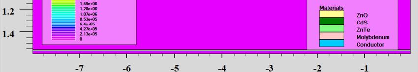
CONSILIO 2020                                                                                                     IOP Publishing
Journal of Physics: Conference Series                         1714 (2021) 012020            doi:10.1088/1742-6596/1714/1/012020

       Cut-line Analysis and Parameters’ Extraction of Zinc Telluride Absorber
       Material based Multi-layer Solar Cell

                          Paritosh Chamola1 and Poornima Mittal2
                          1,2
                            Department of Electronics and Communication Engineering, Delhi Technological University, New
                          Delhi, India
                          paritoshchamola@gmail.com1, poornima2822@gmail.com2

                          Abstract In present paper the ZnTe (Zinc Telluride) solar cell with heterojunction structure is
                          developed and its electrical performance are explored. The ZnTe act as an absorber type layer,
                          CdS (Cadmium-Sulphide) is the buffer layer and ZnO (Zinc-Oxide) is the window type layer in
                          our solar cell. The numerical studies were done using Silvaco-Atlas which is a mathematical
                          device-simulator. The ZnTe solar cell is simulated and various devices parameters such as open
                          circuit voltage, fill factor etc. are extracted on different absorber-layer thickness sweeping from
                          0.5 to 2.5 µm keeping the thickness of other layers constant. This is followed by cutline
                          investigation of the Zinc Telluride solar cell so as to comprehend the device’s physical science as
                          photovoltaic cell. The solar cell is examined via a parallel (i.e. horizontal) cut-line drown inside
                          ZnTe absorber type layer the of photovoltaic cell positioned at the junction of the absorber type
                          and buffer type layer. The ZnTe solar cell shows good performance with 62.89% fill factor.

       1. Introduction
       The solar energy as of today is the best alternate renewable source of energy and the photovoltaic
       cells are the best for the capturing sunlight, an ecofriendly and renewable form of energy. The thin
       film photovoltaic cell built on semiconductor are enormously effective and affordable devices. The
       solar cells function is that of converting solar energy to electric current or electric form of energy. The
       photoelectrons produce light, photons contain energy that differs according to the wavelength of the
       light. In the semiconductor materials the photos are able to generate electric current when they are
       carrying enough energy so as to incite a loosely bound electron (after the electron acquires sufficient
       energy) present in the valance band to the conduction.

                For designing a solar-cell the mathematical simulation models are tools of vital importance.
       Their importance can be understood from the fact that all the understanding of solar cell operation and
       all the needed solar cell improvements for future applications are very often contributed by these
       models [1]. Semiconductors solar cell based especially on group II-VI elements are leaders/best in the
       realization of affordable photovoltaic cells. Zinc telluride (ZnTe) shows a band-gap of 2.23eV to 2.28
       eV [2] and the reported affinity of electron is at 3.73 eV [3] & zinc blend type of crystalline structure.
                The first-generation solar cells are implemented using wafers. These cells are of single crystal
       structure. The thin films and semiconductor deposition with use of glass substrate characterised the
       second generation of the solar cell. In the solar cells which are based on semiconductors the photons
       which have energy lower than energy band gap of absorber layer material are not absorbed and are

              Content from this work may be used under the terms of the Creative Commons Attribution 3.0 licence. Any further distribution
              of this work must maintain attribution to the author(s) and the title of the work, journal citation and DOI.
Published under licence by IOP Publishing Ltd                          1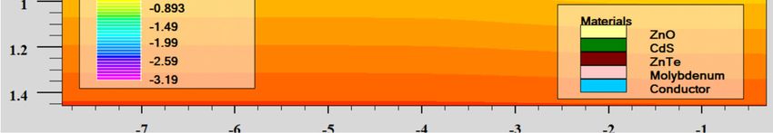
CONSILIO 2020 IOP Publishing
Journal of Physics: Conference Series 1714 (2021) 012020 doi:10.1088/1742-6596/1714/1/012020
lost, thus there is energy wastage. The third generation of solar cells are characterised by intermediate
band solar cell. The intermediate band is created through alloying of the host and mismatched
elements [4]. In the present work Zinc telluride solar cell is studied using the parameters [5-7],
simulation is performed in silvaco atlas device simulator for the solar cell.
The present paper is arranged in four sections beginning with introduction as Section-1.
Further, Section-2 represents structure of solar cell, materials utilised in diverse layers of cell,
furthermore it (cell) is presented by analysing the of performance of Zinc Telluride based solar-cell
and parameter extraction [8]. Afterward, the horizontal cutline internal analysis [9] is demonstrated in
Section-3. Finally, significant results are briefed in Section-4.
2. Electrical characterization of Zinc Telluride Solar cell
The device characteristics are observed using Silvaco Atlas as device simulator. Silvaco being a 2-D
simulator presents a very detailed device physics. In the simulator user defined materials are allowed,
a variety of model parameters are also included for example SRH (Shockley-Read-Hall) model,
Poole-Frenkel mobility model etc., for model calculations mesh is used. High density of meshing
results in better accuracy with an extended run time.
Figure 1. Zinc Telluride based solar-cell
The solar-cell can be simulated in the photovoltaic cell very efficiently. The accuracy of the
solar cell simulation while modelling in Silvaco software attributes to the amalgamation of the
availability of various types of optical propagation model [10] which are extremely accurate and
capability of device simulator. The figure 1 represents the solar-cell simulated in the present paper.
The nature and purpose of the solar cell are the two major factors according to which optical
propagation models are selected and are absolutely dependent on it.
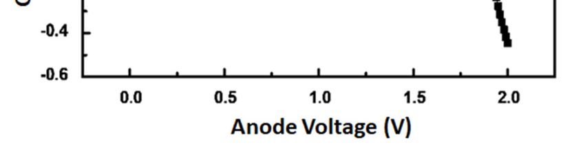
The figure 2 (a) below represents current-voltage graph of Zinc-Telluride/Cadmium-
Sulphide/Zinc Oxide solar cell [11,12]. The photovoltaic cell is irradiated thru AM 1.5 (1 sun). The
incident photon/s start to produce the charge carriers and the current starts to flow. The current
voltage graph of a photovoltaic cell principally represents a graphic description amid photovoltaic
device’s current and voltage at specific state of the illumination. The plot trails the universal current-
voltage shape of any solar-cell.
Open circuit voltage (VOC) is the highest value of voltage provided via a photovoltaic cell
while its connection’s aren’t fixed at all to a external load. The curve in figure 2 (b) between the VOC
and absorber thickness represents that as the absorber thickness is increased open-circuit voltage
increases simultaneously. The VOC displays rectilinear increase as thickness of absorber layer is
increased from 0.5-1.0 μm and 2.0-2.5 μm it remains constant between 1.0-1.5 µm. The highest
magnitude obtained is 1.89 V at an thickness of 2.5 µm.
2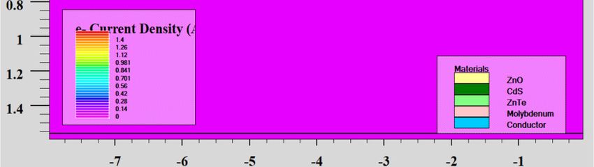
CONSILIO 2020                                                                                       IOP Publishing
Journal of Physics: Conference Series                1714 (2021) 012020       doi:10.1088/1742-6596/1714/1/012020

                               (a)                                                    (b)

                              (c)                                                       (d)
    Figure 2. Characterisation plots of (a) Cathode Current v/s Anode Voltage at Zinc-Telluride layer of
    1.5 µm, (b) Voc, (c) Fill Factor & (d) JSC as a function of absorber layer thickness for Zinc-Telluride
                                               Photovoltaic cell.

             The figure 2 (c) represents the JSC curve for the Zinc-Telluride based solar-cell. The curve
    shows the variation of ISC density with respect to variation in the Zinc telluride thickness i.e. absorber
    thickness. The above curve represents the fact that the JSC increases with the absorber thickness. As
    expected, current density (Jsc) increases as absorber thickness is increased. In the solar cell, we
    define current density to study how much current can be generated in photovoltaic cells because of
    it’s normalized by means of area of our active layer (including metal electrode).

             The figure 2 (d) represents the curve between the FF (fill factor) and the absorber layer
    thickness. FF is an important parameter representing relation among real max. power delivered via a
    photovoltaic cell under steady operating settings & is equal to the product between VOV & ISC. Values
    of fill-factor present quality of photovoltaic cell. The nearer is the magnitude of fill-factor to unity,
    means additional power could be delivered through photovoltaic cell making fill-factor a significant
    parameter for a solar cell. The typical values in general for the solar cells are in between 0.7 to 0.8, in
    the above graphical representation shows that the fill factor increases with the absorber thickness with
    fill factor values varying from 0.54 to 0.68 for a ZnTe cell when thickness is varied from 0.5 to 2.5
    µm.
    3. Internal Analysis
    In the earlier section the ZnTe cell was simulated and its corresponding parameters such as Voc, FF
    etc. were extracted. Here in the present section the internal investigation of the solar-cell is made so as

                                                           3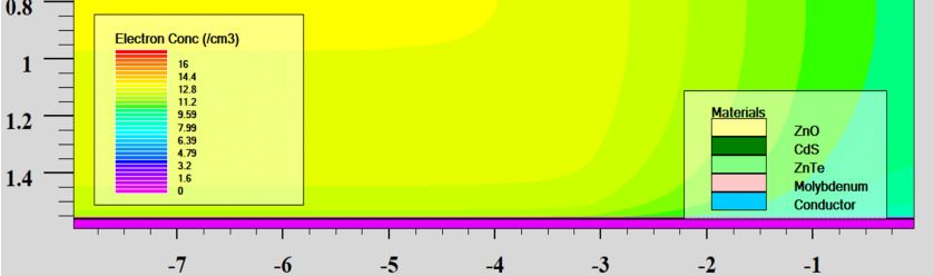
CONSILIO 2020 IOP Publishing
Journal of Physics: Conference Series 1714 (2021) 012020 doi:10.1088/1742-6596/1714/1/012020
to understand, explore and examine the internal developments linked to the architecture. This
understanding and thoughtful investigation of the device physics help to analyse and appreciate the
behaviour of the devices i.e. solar cells in depth. This analysis in turn helps to prove the influence or
role of each layer in the solar cell specially with respect to the solar-cell performance.
Starting with the electric field, electric field variation in volt/cm of the device is shown in
figure 3. The electric field is further more established between absorber type and buffer type layer (at
junction) maximizing towards right near to the electrode and drops in value as the distance rises from
junction which settles the fact that majority of carriers continue to be concentrated in the juxtaposition
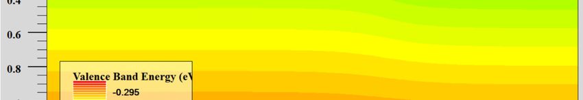
of electrode, at top of buffer layer. The valance band energy is represented in figure 4. The photons
create electron hole pairs when light is incident of the device, the created electron move towards the
conduction band (CB) from valance (VB) for the correct device operation.
Figure 3. Variation of the applied electric field (V/cm) in layers of solar cell
Figure 4. Layer-wise valance band energies distribution for ZnTe cell.
The figures 5 (a) & (b) below represents the variation of the electron concentration & the electron
current variation. In the presented device the CdS layer is buffer layer and ZnTe is absorber layer. The
maximum electron current density obtained is 1.4 A/cm2.
4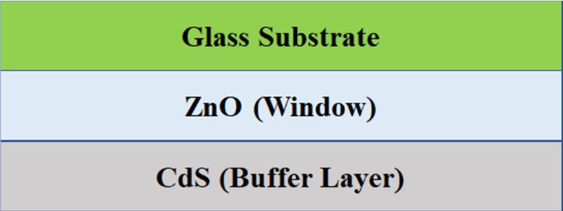
CONSILIO 2020                                                                                    IOP Publishing
Journal of Physics: Conference Series              1714 (2021) 012020      doi:10.1088/1742-6596/1714/1/012020

                            (a)                                                      (b)
         Figure 5. Device structures portraying layer wise variation of (a) Density of electron current and
                                          (b) Concentration of electron.
    The purpose of absorber type layer in the thin film photovoltaic cell is to capture incident photon/s
    and produce charge carriers. Whereas, function of buffer is to form a junction with absorber type layer
    & to transport the photoelectrons.
    Conclusion
    The present paper focuses on the study of the Zinc telluride solar. At first an already presented ZnTe
    based solar cell is simulated and its analytical and cutline analysis is also performed so as to explore,
    investigate and understand the internal device physics of the three solar cells. Parameter such as
    electric field, concentration etc. are also extracted for analysis and verification of the solar cell
    performance. Optimized results are achieved with a fill factor of 82.54%. From theses fundamental
    outcomes, it’s established that enhanced performance can be comprehended from ZnTe solar-cell and
    can deliver a base for upcoming progress of Solar-cells which are based on Zinc Telluride materials.

    References
        [1] N. Amin, K. Sopian, M. Konagai 2007 Numerical modeling of CdS/CdTe and
            CdS/CdTe/ZnTe solar cells as a function of CdTe thickness Solar Energy Materials and Solar
            Cells, 91(13), 1202-1208.
        [2] A. Kaneta, S. Adachi 2000 Photoreflectance study in the E-1 and E- 1+Delta (1) transition
            regions of ZnTe J. Phys. D: Appl. Phys. 33(8) 901-905.
        [3] A. Pistone, A. S. Arico, P. L. Antonucci, D. Silvestro, V. Antonucci 1998 Preparation and
            characterization of thin film ZnCuTe semiconductors Sol. Energy Mater. Sol. Cell., 53, 255-
            267.
        [4] Y. H. Khattak, F. Baig, S. Ullah, B. Marí, S. Beg, H. Ullah 2018 Enhancement of the
            conversion efficiency of thin film kesterite solar cell Journal of Renewable and Sustainable
            Energy 10, 033501.
        [5] K. Mukhopadhyay, P. F. H. Inbaraj, J. Joseph Prince 2018 Thickness optimization of
            CdS/ZnO hybrid buffer layer in CZTSe thin film solar cells using SCAPS simulation program
            Materials Research Innovations, 6, 319-329.
        [6] S. Negi, P. Mittal, B. Kumar 2019 Analytical modelling and parameters extraction of
            multilayered OLED IET Circuits Devices Syst., 13(8), 1255-1261.
        [7] S. Negi, P. Mittal, B. Kumar 2018 Impact of different layers on performance on performance
            of OLED, Microsyst. Technol. 24 (12) 4981-4989.
        [8] ATLAS (2014) ATLAS User’s Manual Device Simulation Software, Silaco International Ltd,
            Santa Clara.
        [9] P. Mittal, Y.S. Negi, R.K. Singh 2015 An analytical approach for parameter extraction in
            linear and saturation regions of top and bottom contact organic transistors J. Comput.
            Electron., 14, 828-843.
        [10]         P. Mittal, Y. S. Negi, R. K. Singh 2015 Mapping of performance limiting issues to
            analyze top and bottom contact organic thin film transistors Journal of Computational
            Electronics 14, 360-379.
        [11]         F. A. Jhuma, M. J. Rashid 2020 Simulation study to find suitable dopants of CdS
            buffer layer for CZTS solar cell J Theor Appl Phys 14, 75-84.
        [12]         P. R. Nikam, P. K. Baviskar, J. V. Sali, K. V. Gurav, J. H. Kim, B. R. Sankapal 2016
            CdS surface encapsulated ZnO nanorods: synthesis to solar cell application J. Alloy. Compd.
            689, 394-400.

                                                         5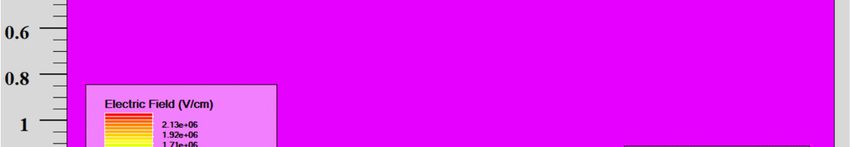
You can also read