Deep Sub-Electron Read Noise in Image Sensors Using a Multigate-Source-Follower (InvitedPaper)
←
→
Page content transcription
If your browser does not render page correctly, please read the page content below
This article has been accepted for inclusion in a future issue of this journal. Content is final as presented, with the exception of pagination.

              IEEE TRANSACTIONS ON ELECTRON DEVICES                                                                                                                     1

        Deep Sub-Electron Read Noise in Image
       Sensors Using a Multigate-Source-Follower
                                                             (Invited Paper)
                       Wei Deng , Student Member, IEEE, and Eric R. Fossum , Fellow, IEEE

   Abstract — As the in-pixel source-follower (SF) gate size                                      The SF transistor output noise is generally composed of
scales down in CMOS image sensors (CISs) and quanta                                            thermal noise, random telegraph noise (RTN), and 1/ f noise.
image sensors (QISs), the pixel conversion gain (CG)                                           The well-known models, such as the McWhorter number fluc-
increases at the cost of more 1/f noise. In this article, a multi-
gate SF (MGSF) is proposed to simultaneously increase                                          tuation model [4], Hooge mobility fluctuation model [5], or the
pixel CG and reduce 1/f noise. The MGSF improves the                                           Berkeley unified 1/ f noise model [6], have been developed to
tradeoff between 1/f noise and CG that exists for pixels with                                  model the 1/ f noise, although none of them is universally
conventional SFs, leading to reduced input-referred read                                       accepted. Experimental data previously obtained from a QIS
noise at deep sub-electron levels.                                                             prototype chip with small SF show that the mobility fluctuation
  Index Terms — 1/f noise, CMOS image sensor (CIS), multi-                                     model matches the best in that case [7].
gate source-follower (MGSF), quanta image sensor (QIS).                                           No matter from where the 1/ f noise originates, it is widely
                                                                                               observed that 1/ f noise scales inversely with transistor gate
                                                                                               area so that an SF with a larger gate area has a lower 1/ f
                         I. I NTRODUCTION
                                                                                               noise [8]. However, a larger area will lead to a larger SF

T     HE input-referred read noise of CMOS image sen-
      sors (CISs) has steadily improved over the past several
decades. In this sensor, photosignal charge is collected and
                                                                                               gate parasitic capacitance, which will cause a larger total
                                                                                               FD parasitic capacitance and thus lower the CG. Therefore,
                                                                                               to achieve a higher CG, a smaller gate area is desired. Due
then transferred to a floating-diffusion (FD) sense node, and                                  to this tradeoff between 1/ f noise and CG, the input-referred
the change in voltage on the sense node is buffered by a                                       read noise can only achieve a theoretically limited minimum
source-follower (SF) transistor. The electron input-referred                                   level when the SF is sized at its optimum [7].
read noise is determined by the SF voltage noise divided by                                       The tradeoff between 1/ f noise and CG makes it difficult to
the output conversion gain (CG), (volts/e− ) of the sense node,                                further reduce the input-referred read noise at the pixel level.
and SF. The CG is inversely proportional to the total sense                                    To improve this tradeoff, a new SF structure was conceived [9].
node capacitance. The CMOS Quanta Image Sensor (QIS), a                                        In this article, a multigate SF (MGSF) is designed and fab-
special type of photon-counting CIS with deep sub-electron                                     ricated with the aim to simultaneously increase the pixel CG
input-referred read noise obtained by using high CG, has                                       and reduce the 1/ f noise.
achieved read noise as low as 0.12-e− rms in some pixels at
room temperature although the median noise across all pixels
was 0.22-e− rms [1]. This enables good detection of single                                                                       II. P IXEL D ESIGN
electrons without the use of avalanche multiplicative gain. The                                   The conventional SF in a CIS/QIS pixel is replaced with
goal is for all pixels to achieve input-referred read noise of less                            an MGSF. The MGSF consists of the SF modulation gate
than 0.15-e− rms so that accurate (low bit-error rate) single-                                 (MG), i.e., the FD-connected input gate, and one or two dc-
photoelectron counting can be performed since the bit-error                                    biased guard gates (GG). Conceptually, the GG is introduced
rate drops rapidly with read noise [2]. The specialized QIS                                    to increase the total effective SF gate area for 1/ f noise
pixel is referred to as a jot [3].                                                             reduction, while the SF modulation gate can be the minimum
                                                                                               size allowed to achieve a higher CG.
  Manuscript received January 19, 2022; revised March 20, 2022;
accepted April 5, 2022. This work was supported in part by the Jet                                Three MGSF configurations are explored. The GG of an
Propulsion Laboratory under Grant RSA 1658937, in part by the NASA                             MGSF can be placed closer to the source end (configuration
Award Subcontract from Rochester Institute of Technology under Grant                           version V1) or the drain end (V2). The MGSF can also have
80NSSC20K0310. The review of this article was arranged by Editor
D. Van Blerkom. (Corresponding author: Wei Deng.)                                              two GGs, while the modulation gate is placed in-between
  The authors are with the Thayer School of Engineering, Dartmouth                             (V3). Since the modulation gate is separated from the GG, the
College, Hanover, NH 03755 USA (e-mail: wei.deng.th@dartmouth.edu).                            parasitic capacitance between the SF drain/source and the GG
  Color versions of one or more figures in this article are available at
https://doi.org/10.1109/TED.2022.3166723.                                                      will not contribute much to FD total capacitance. The width
  Digital Object Identifier 10.1109/TED.2022.3166723                                           of MG/GG is 0.14 μm and the length of MG is 0.27 μm

This work is licensed under a Creative Commons Attribution 4.0 License. For more information, see https://creativecommons.org/licenses/by/4.0/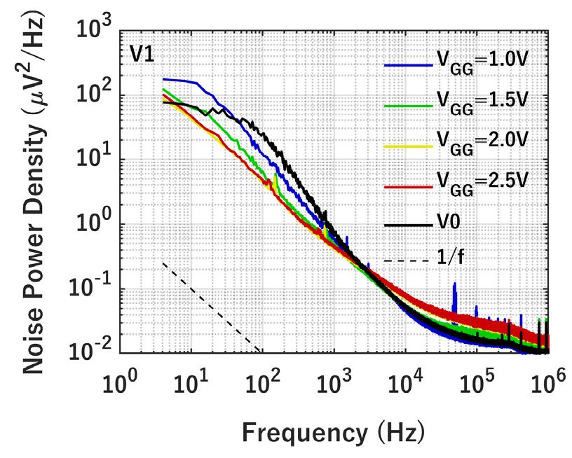
This article has been accepted for inclusion in a future issue of this journal. Content is final as presented, with the exception of pagination.
2 IEEE TRANSACTIONS ON ELECTRON DEVICES
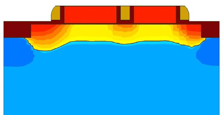
Fig. 3. Cross-sectional view of the simulated doping profile of a
buried-channel MGSF V2 in TCAD. Red indicates N-doped and blue
indicates P-doped.
Fig. 1. Schematic: (a) V0 SF, (b) MGSF V1, (c) MGSF V2, and
(d) MGSF V3.
Fig. 4. Operation potential-well diagram of (a) V0 SF, (b) MGSF V1,
(c) MGSF V2, and (d) MGSF V3.
is implemented to further reduce the parasitic overlap capaci-
tance between the reset gate and the FD [11].
The doping profile of a buried-channel MGSF V2 is simu-
lated in TCAD and the cross-sectional view is shown in Fig. 3
Fig. 2. Layout: (a) V0 SF, (b) MGSF V1, (c) MGSF V2, and as an example. An N-type layer can be seen in the channel
(d) MGSF V3. region, which forms the buried channel. Self-aligned process
is used to dope the source, drain, and the gap region. The gap
for all MGSFs. The length of GG is 0.32 μm for V1/V2 between the modulation gate and the GG is filled by spacer.
and 0.27 μm for V3 due to limited space. The as-drawn gap The potential-well diagrams of the MGSFs in operation
between gates is 0.13 μm and may be comparable within are shown in Fig. 4. Fig. 4(a) corresponds to V0 SF, which
2–3× to the mean free path of an electron in the channel shows the potential-well diagram when the gate is turned on.
[10]. A conventional MOSFET SF with the same total gate As shown in Fig. 4(b), the modulation gate is biased at a
area as V1 and V2 is included for baseline reference (V0 slightly lower voltage than the GG. The gap between MG and
SF configuration). Since the buried-channel SF generally has GG forms a deeper potential well and is filled with charge
lower 1/ f noise [7], all MGSF configurations and the V0 SF carriers. The potential-well diagrams of MGSF V2 and V3
are buried-channel devices. are shown in Fig. 4(c) and (d), respectively.
The schematics of V0 SF and three versions of MGSF Correspondingly, Fig. 5 shows the electrostatic potential
are shown in Fig. 1(a)–(d), and the corresponding layouts are along the channel of the MGSFs in operation based on
shown in Fig. 2(a)–(d). A 1 × 2 shared readout circuitry is TCAD simulation. Fig. 5(a) shows the electrostatic potential
used. As illustrated in both the schematic and layout, the profile of V0 SF when the modulation gate is turned on.
pump-gate jot with a distal FD is implemented to elimi- For MGSF V1, the modulation gate is biased at a slightly
nate the parasitic overlap capacitance between the transfer lower voltage than the GG. Its electrostatic potential profile is
gate (TG) and FD [11]. The jot storage well (SW) is located shown in Fig. 5(b). The undulation is due to doping changes.
underneath the TG. The punchthrough reset (PTR), which The electrostatic potential profiles of MGSF V2 and V3 are
eliminates the reset gate between FD and the reset drain (RD), shown in Fig. 5(c) and (d), respectively.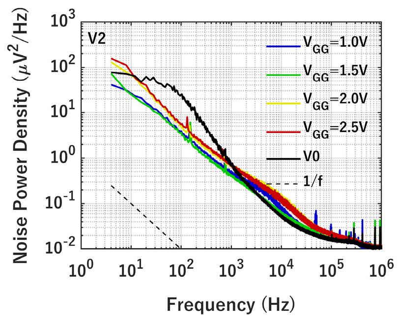
This article has been accepted for inclusion in a future issue of this journal. Content is final as presented, with the exception of pagination.
DENG AND FOSSUM: DEEP SUB-ELECTRON READ NOISE IN IMAGE SENSORS USING MGSF 3
TABLE I
S UMMARY OF E XTRACTION R ESULTS FROM TCAD S IMULATION
AND THE M EASURED SF G AIN
Fig. 5. Electrostatic potential along channel of (a) V0 SF, (b) MGSF V1,
(c) MGSF V2, and (d) MGSF V3. Undulations are due to doping changes.
MG and GG are biased at 1.4 and 1.5 V, respectively.
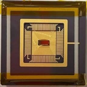
Fig. 7. QIS test chip.
Fig. 8. Schematic of the readout signal chain with the conventional SF
configuration.
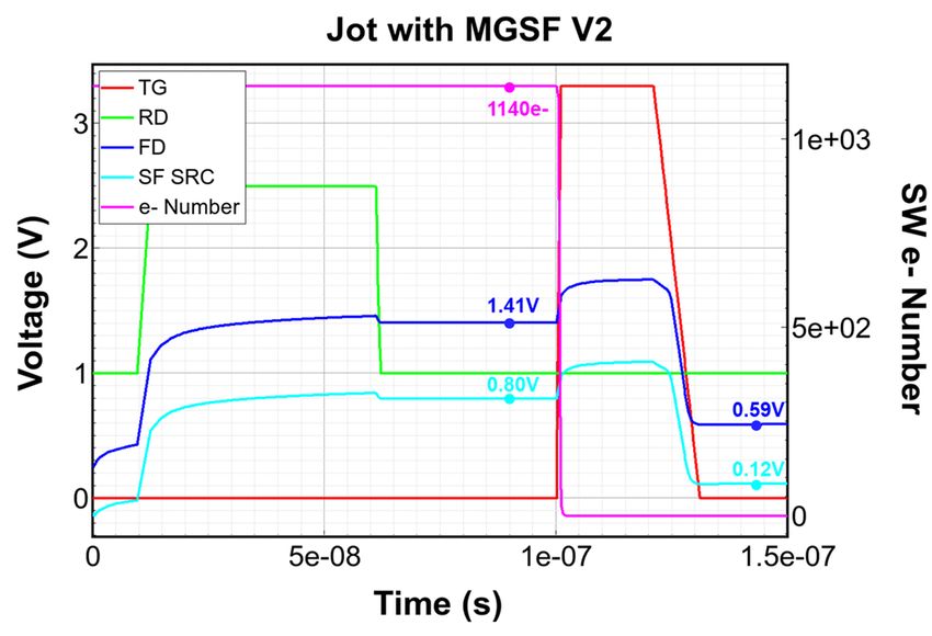
Fig. 6. Transient simulation of a jot with MGSF V2 in TCAD used to The QIS test chip within a ceramic pin grid array pack-
estimate CG including parasitics. (SRC: Source.) age is shown in Fig. 7. Fig. 8 shows the schematic of the
readout chain. The pixel output is sent to a correlated double
Operation of MGSF V2 was simulated using Sentaurus sampling (CDS) circuit, followed by a unity-gain buffer.
TCAD, as shown in Fig. 6. When the TG is pulsed, 1140 e− A subsequent programmable gain amplifier (PGA) is utilized
is transferred from the photodiode SW to the FD, causing to amplify the signal, with a switchable analog gain that ranges
an FD voltage drop of 0.82 V (i.e., from 1.41 to 0.59 V). from 2 to 40 V/V. The output of the PGA is then sent to
Therefore, the input-referred CG is calculated to be 716 another unity-gain amplifier, which drives the output pads so
μV/e− . A summary of extraction results from all types of the signal can be read out off-chip. The signal is then digitized
SF devices is shown in Table I. The extracted input-referred by an off-chip analog-to-digital converter (ADC). The gain of
CG of MGSFs (e.g., 700 μV/e− for V1, 716 μV/e− for V2, the PGA is set to be 10 V/V during the 1/ f noise testing.
and 709 μV/e− for V3) is about 20% higher than that of Fig. 9 shows the 1/ f noise spectrum measurement timing
the V0 SF (e.g., 579 μV/e− ) since the size of the MGSF diagram. First, the pixel is reset by turning on both the TG and
modulation gate is smaller compared to the V0 SF gate. the reset gate. Then, the PGA continuously samples the pixel
According to the previous experimental verification [11], a output signal for 0.25 s with a sampling period of 0.5 μs;
CG that is ∼20% smaller than the simulated CG is expected 500 000 samples are collected for each pixel. The data are
in fabricated devices due to other factors that are not consid- digitized by an off-chip ADC and a data acquisition card saves
ered in simulation. The electron input-referred read noise is the digitized data in a PC memory. The fast Fourier transform
estimated using the mobility fluctuation model and total MGSF (FFT) algorithm was used to convert the data from the time
gate area. domain to the frequency domain. A noise spectrum can thus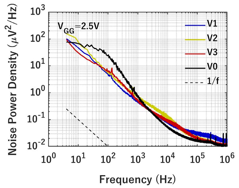
This article has been accepted for inclusion in a future issue of this journal. Content is final as presented, with the exception of pagination.
4                                                                                                                                  IEEE TRANSACTIONS ON ELECTRON DEVICES

Fig. 9. Timing diagram for noise measurement.

be constructed. The input-referred noise power spectra are
obtained by dividing the measured output noise spectra by
the gain of the readout circuit.

             III. C HARACTERIZATION R ESULTS
   The QIS with MGSFs is implemented in a TSMC 45/65 nm
stacked backside-illuminated (BSI) CIS baseline process. The
pixel pitch is 2.2 μm × 1.1 μm. PTR operation was expected,
but the PTR structure was found to be always “ON” with RD
shorted to the SF gate, perhaps due to implant conditions.
Measurement of read noise by the photon-counting histogram
technique [12] was thus not possible. However, the imple-
mentation defect meant we could directly access the SF gate
for voltage-domain measurements. The gain and noise for all
types of MGSFs were tested. A total of 32 devices of each                                     Fig. 10. Gain measurement for four types of SFs. (a) Transfer curves.
type were measured.                                                                           (b) SF gain histograms.

A. MGSF Gain                                                                                  the dashed line as a reference. The bias current for all SFs
                                                                                              is 1 μA. Fig. 11(a) shows that the MGSFs have lower noise
   The gain measurement results for four types of SFs are
                                                                                              compared to the V0 SF when the GG is biased at 1.5 V.
shown in Fig. 10. Fig. 10(a) shows the measured average of
                                                                                              This indicates that splitting a larger SF gate into a smaller
transfer curves from 32 SFs of each type. The GG is biased at
                                                                                              modulation SF gate plus a GG seems to reduce the overall 1/ f
a dc voltage of 2.5 V for MGSF. The conventional MOSFET
                                                                                              noise—a surprising result since nominally one might expect
SF and the MGSF configurations show similar transfer char-
                                                                                              similar 1/ f noise power for devices with the same total gate
acteristics. The SF gain can be extracted by measuring the
                                                                                              area.
slope of the linear region of the transfer curve. Although the
                                                                                                 The apparent change in exponent α in the 1/ f α dependence
gain of the V0 SF is slightly higher (e.g., 0.78), the gain of
                                                                                              is also noteworthy where α is close to unity in the V2 and
the MGSFs is similar (e.g., 0.76 for V1 and V3 and 0.77 for
                                                                                              V3 MGSF configurations, but α ≈ 1.5 for the “normal” V0
V2). The gain generally matches the TCAD simulation result
                                                                                              SF configuration, possibly indicating a change in underlying
although it is 9% smaller, possibly due to the discrepancy
                                                                                              physical mechanism for the noise. (The exponent is α ≈ 1.2 for
between the process flow used in simulation and fabrication.
                                                                                              the V1 configuration.) We might further speculate that since
The output voltage of MGSFs is higher than that of the V0 SF,
                                                                                              the exponent changes mostly for V2 and V3, the mechanism
due to the GG biased at a slightly higher voltage lowering the
                                                                                              may be related to the drain (pinchoff) end of the MOSFET.
threshold voltage of MGSFs. The extracted SF gain and the
                                                                                                 The results show the same trend when the GG is biased at
measured gain are summarized in Table I. Fig. 10(b) shows
                                                                                              2.5 V, as shown in Fig. 11(b). It is observed that the variation
the histograms of the measured gain for all SFs. The MGSFs
                                                                                              of the individual noise spectrum among all 32 SFs from each
have similar gain variations as the conventional V0 SF. Normal
                                                                                              SF type is relatively large (about an order of magnitude),
SF operation is maintained for MGSFs with the extra GG.
                                                                                              probably due to the small gate size and thus relatively large
                                                                                              variations in geometry, doping, and scattering center distribu-
B. 1/f Noise Spectrum                                                                         tion during fabrication. In the high-frequency region, the noise
   The input-referred noise power spectra for four types of                                   spectrum flattens out because of the white noise (e.g., thermal
SFs are shown in Fig. 11. Each curve is an average of the                                     noise). Correlated multiple sampling (CMS) may be utilized
results from 32 devices. The 1/ f trend is also shown using                                   to suppress the high-frequency noise.
This article has been accepted for inclusion in a future issue of this journal. Content is final as presented, with the exception of pagination.
DENG AND FOSSUM: DEEP SUB-ELECTRON READ NOISE IN IMAGE SENSORS USING MGSF 5
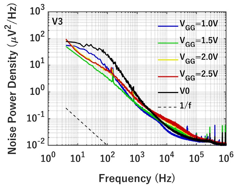
Fig. 11. Input-referred noise spectra for four types of SFs with different
GG bias voltages (SF modulation gate bias voltage VMG = 1.5 V and
bias current Ib = 1 µA). (a) VGG = 1.5 V and (b) VGG = 2.5 V.
The impact of the GG bias voltage VGG is shown in
Fig. 12. For buried-channel SFs, the height of the potential
barrier between the channel and the Si–SiO2 interface changes
since the surface potential increases monotonically from the
source to the drain. Due to the higher bias on the drain end,
the potential barrier is higher on the drain end, leading to
better shielding of the interface. Therefore, the GG may have
different impact on the noise when placed on the drain end or
the source end.
Fig. 12(a) shows the input-referred noise spectra of MGSF
V1 at different GG bias voltages. The 1/ f noise decreases Fig. 12. Input-referred noise spectra of four types of SFs at different GG
when the GG is biased at a higher voltage. It indicates that bias voltages (SF modulation gate bias voltage VMG = 1.5 V and bias
current Ib = 1 µA). (a) MGSF V1, (b) MGSF V2, and (c) MGSF V3.
the 1/ f noise spectrum can be modulated by the GG bias
voltage. When the GG (closer to the source end) is biased
at a higher voltage, the potential barrier between the channel which is the opposite compared to MGSF V1. This is probably
and the Si–SiO2 interface will be lowered, and intuitively, the because the lower the GG (closer to the drain end) voltage,
noise will be higher due to weaker shielding. However, the the potential barrier seen by the buried channel is higher, and
observed noise is lower at higher VGG , which indicates that thus, the 1/ f noise is smaller.
there might be another mechanism other than shielding. For The input-referred noise spectra of MGSF V3 at different
example, higher VGG may lead to more inversion charge and GG bias voltages are shown in Fig. 12(c). Similarly, the 1/ f
thus less charge number variation or less noise. noise is VGG dependent. However, no clear trend is observed,
For different versions of MGSF, the influence of the GG probably because there are GGs on both the drain end and the
bias is different. As shown in Fig. 12(b), for MGSF V2, the source end, which combines the two opposite noise effects
1/ f noise decreases when the GG is biased at a lower voltage, observed in Fig. 12(a) and (b).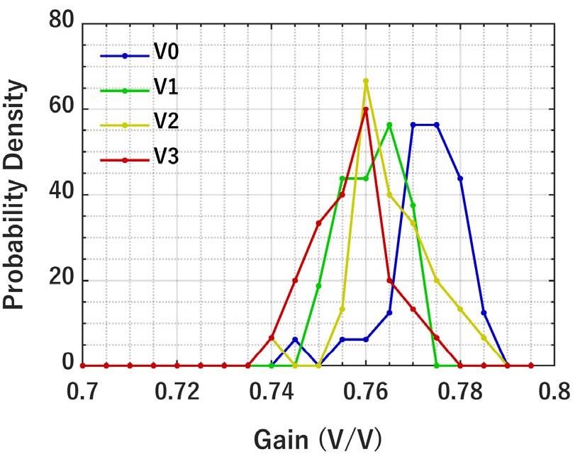
This article has been accepted for inclusion in a future issue of this journal. Content is final as presented, with the exception of pagination.
6                                                                                                                                 IEEE TRANSACTIONS ON ELECTRON DEVICES

   To achieve the lowest noise, the optimum GG bias voltage                                  the support from NASA and the collaboration with Rochester
should be used. Overall, compared to the MGSFs with differ-                                  Institute of Technology under Dr. Don Figer. Recent con-
ent GG bias voltages VGG , the V0 SF has a similar or higher                                 versations with Prof. Jifeng Liu with Dartmouth are also
1/ f noise.                                                                                  appreciated.
           IV. D ISCUSSION AND C ONCLUSION
                                                                                                                                      R EFERENCES
   These surprising results generate many questions that need
                                                                                              [1] J. Ma, D. Zhang, O. A. Elgendy, and S. Masoodian, “A 0.19 e-RMS
to be explored through additional experiments in the future.                                      read noise 16.7 Mpixel stacked quanta image sensor with
For example, how is the 1/ f noise affected by the intergate                                      1.1 μm-pitch backside illuminated pixels,” IEEE Electron Device
gap size? Is it related to the mean free path of the channel                                      Lett., vol. 42, no. 6, pp. 891–894, Jun. 2021, doi: 10.1109/LED.
                                                                                                  2021.3072842.
electrons? Why does it not matter too much if the GG is on the                                [2] E. R. Fossum, “Modeling the performance of single-bit and multi-bit
source end or drain end? How is the MGSF different from two                                       quanta image sensors,” IEEE J. Electron Device Soc., vol. 1, no. 9,
transistors in series connected by merged source–drain such as                                    pp. 166–174, Sep. 2013, doi: 10.1109/JEDS.2013.2284054.
                                                                                              [3] J. Ma and E. R. Fossum, “A pump-gate jot device with high conversion
the normal relationship between the SF and select transistor in                                   gain for a quanta image sensor,” IEEE J. Electron Devices Soc., vol. 3,
typical CIS devices? Or do conventional CIS devices already                                       no. 2, pp. 73–77, Mar. 2015, doi: 10.1109/JEDS.2015.2390491.
benefit from the two transistors in series with respect to 1/ f                               [4] A. L. McWhorter, “1/f noise and related surface effects in germanium,”
                                                                                                  Ph.D. dissertation, Dept. Elect. Eng., MIT, Cambridge, MA, USA, 1955.
noise? Can the MGSF be successfully implemented in a less                                     [5] F. N. Hooge, “1/f noise is no surface effect,” Phys. Lett A, vol. 29, no. 3,
advanced technology node with a larger gap between gates?                                         pp. 139–140, Aug. 2002, doi: 10.1016/0375-9601(69)90076-0.
And, of course, one needs to demonstrate that the MGSF                                        [6] K. K. Hung, P. K. Ko, C. Hu, and Y. C. Cheng, “A unified model for
                                                                                                  the flicker noise in metal-oxide-semiconductor field-effect transistors,”
actually improves input-referred read noise in fully functional                                   IEEE Trans. Electron Devices, vol. 37, no. 3, pp. 654–665, Mar. 1990,
pixels?                                                                                           doi: 10.1109/16.47770.
   An image sensor pixel with an MGSF is introduced in this                                   [7] W. Deng and E. R. Fossum, “1/f noise modelling and characterization
                                                                                                  for CMOS quanta image sensors,” Sensors, vol. 19, no. 24, p. 5459,
article. Compared to the conventional MOSFET SF with the                                          Dec. 2019, doi: 10.3390/s19245459.
same total gate area, the MGSF shows similar or lower noise.                                  [8] M.-H. Tsai and T.-P. Ma, “The impact of device scaling on the current
The bias voltage of the MGSF GG can be used to optimize                                           fluctuations in MOSFET’s,” IEEE Trans. Electron Devices, vol. 41,
                                                                                                  no. 11, pp. 2061–2068, Nov. 1994, doi: 10.1109/16.333823.
the 1/ f noise. The MGSF has a higher CG compared to the                                      [9] W. Deng and E. R. Fossum, “Multi-gate source-follower for quanta
conventional SF due to the small size of the modulation gate,                                     image sensors (QIS),” in Proc. Int. Image Sensor Workshop, Sep. 2021,
as shown in the TCAD simulation. It appears that higher CG                                        pp. 20–23.
                                                                                             [10] B. Qiu et al., “First-principles simulation of electron mean-
and lower 1/ f noise can be obtained simultaneously, making                                       free-path spectra and thermoelectric properties in silicon,”
MGSF potentially useful for noise reduction in CIS and QIS                                        Europhys. Lett., vol. 109, no. 5, p. 57006, Mar. 2015,
devices.                                                                                          doi: 10.1209/0295-5075/109/57006.
                                                                                             [11] J. Ma, S. Masoodian, D. A. Starkey, and E. Fossum, “Photon-
                        ACKNOWLEDGMENT                                                            number-resolving megapixel image sensor at room temperature without
                                                                                                  avalanche gain,” Optica, vol. 4, no. 12, pp. 1474–1481, Dec. 2017, doi:
  The authors are grateful for the comments from Dr. Jiaju                                        10.1364/OPTICA.4.001474.
Ma with Gigajot Technology, Inc., during the chip design                                     [12] D. A. Starkey and E. R. Fossum, “Determining conversion gain and read
                                                                                                  noise using a photon-counting histogram method for deep sub-electron
phase. They appreciate Taiwan Semiconductor Manufacturing                                         read noise image sensors,” IEEE J. Electron Devices Soc., vol. 4, no. 3,
Corporation for the device fabrication and also grateful for                                      pp. 129–135, May 2016, doi: 10.1109/JEDS.2016.2536719.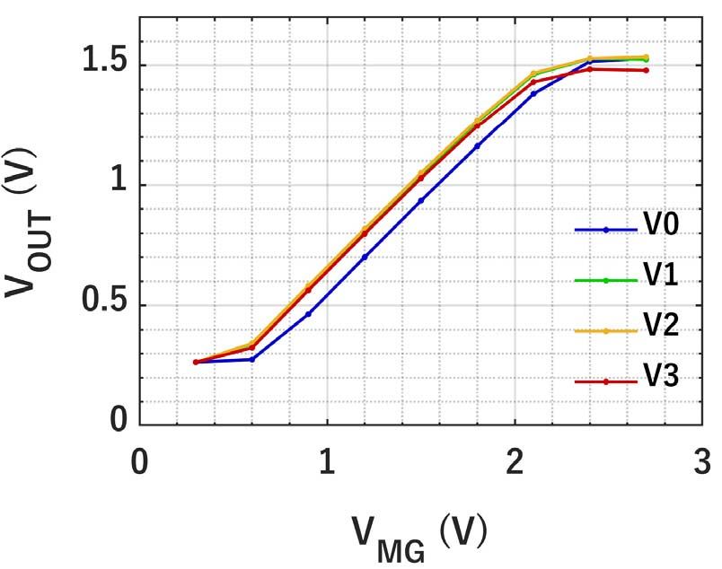
You can also read