Development and Mass-Production of an OLED Lighting Panel - Most-Promising Next-Generation Lighting
←
→
Page content transcription
If your browser does not render page correctly, please read the page content below
Mitsubishi Heavy Industries Technical Review Vol. 49 No. 1 (March 2012)
                                                                                                                     47

             Development and Mass-Production
                  of an OLED Lighting Panel
         - Most-Promising Next-Generation Lighting -

                                                                  KEIICHI HORI*1               JOJI SUZUKI*2

                                                                  MAKOTO TAKAMURA*3            JUNICHI TANAKA*4

                                                                  TSUTOMU YOSHIDA*5            YOSHITAKA TSUMOTO*6

       Lumiotec Inc. is the only company in the world that specializes in the mass-production and
distribution of organic light-emitting diode (OLED) lighting panels, the most-promising
next-generation lighting source. The company started manufacturing and selling a total of 10
models in January 2011. They are available in five shapes (square in two sizes, large and small;
and rectangle in three sizes, large, medium, and small), with each model in two lighting colors
(warm white and natural white). In September 2011, the company also started selling two types of
design luminaires (product names: HANGER and VANITY), incorporating, for the first time in the
world, a mass-produced OLED lighting panel and a dedicated compact driver module. In the
development of the next-generation panels, the company used phosphorescent materials to achieve
a luminous efficacy of 40 lm/W, and developed new panels with high efficiency, high luminance,
and long lifetime.

|1. Introduction
       To study the feasibility of OLED lighting panels, Lumiotec was established in May 2008 as
the world's first company specializing in lighting OLED panels. Investment was provided from
companies such as Mitsubishi Heavy Industries, Ltd. (MHI), Rohm Co., Ltd., Toppan Printing Co.,
Ltd. and Mitsui & Co., Ltd.
       Unlike existing light sources, such as incandescent light bulbs and fluorescent lamps, OLEDs
are planar light emitters that are lightweight and have thin profiles. This allows lamp manufacturers
and designers to create unprecedented designs and provide dramatic effects, leading to the creation
of new living environments in houses, offices, stores, and vehicles such as cars and airplanes.
OLEDs can provide safe and comfortable lighting for general consumers because, unlike
fluorescent lamps, they do not contain mercury or other harmful substances. They emit UV-free
soft light that is gentle on the skin and eyes and has a high color-rendering index.
       Based on multi-photon emission device (MPE) technology and in-line deposition technology
with linear evaporation sources, we constructed a mass-production line in Yonezawa City in
Yamagata Prefecture, Japan, for the development and production of OLED lighting panels. The
former technology is a method to achieve both high luminance and long lifetimes. Typically these
parameters are considered to be in a trade-off relationship. The latter technology is a technique to
significantly increase the efficiency of material use and reduce the time required for multi-layered
film formation.

|2. Development of High-luminance and Long-lifetime Panels
2.1     OLED devices for lighting applications
      An OLED device is a planar light-emitting diode using an organic semiconductor. Taking
advantage of its characteristics, OLED devices were first employed in displays. In recent years,
high expectations have been placed on these devices as next-generation lighting sources, along with

*1 General Manager, Technical Department, Lumiotec Inc.        *2 Chief Engineer, Lumiotec Inc.
*3 General Manager, Development Department, Lumiotec Inc.      *4 Manager, Development Department, Lumiotec Inc.
*5 Manager, Technical Department, Lumiotec Inc.
*6 Manager, Advanced Systems Department, Industrial Machinery Business, Technology & Solutions Division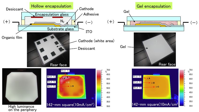
Mitsubishi Heavy Industries Technical Review Vol. 49 No. 1 (March 2012)
48
LED lamps. Because light sources for lamps require luminance more than 10 times that of displays,
achieving both high-luminance and long-lifetime has always been a major challenge. Lumiotec
succeeded in achieving high-luminance uniform light emission over a large panel via the MPE
technology. In this method, multiple layers of emission units are laminated so that the current
efficiency (luminance) is multiplied almost by the number of emission units. An MPE device (the
structure and principle of which are shown in Figure 1) uses a technology to laminate emission
units in series with a charge generation layer interposed inbetween**1. This makes it possible to
simultaneously achieve high-luminance and long-lifetimes.
**1: Joint patent owners are MHI, Rohm, and Professor Kido of Yamagata University.
Lumiotec is the only licensee.
Figure 1 Principle and cross-sectional diagrams of multi-photon emission devices
2.2 Performance required for lighting OLED panels
In addition to their high-luminance and long-lifetime, OLED lighting panels are required to
have high luminous efficacy (units: lm/W) and a high color-rendering index (index of color
reproducibility). They should also be compliant with the standards of lighting colors (color
temperature and chromaticity coordinates). Angular dependence on emission, changes after aging,
and variation among individual devices should also be within a certain range**2. We are trying to
develop a practical product, while keeping in mind that we need to achieve all of these features in a
well-balanced way.
**2: Standards for solid-state lighting colors are mainly intended for LED lamps.
Further discussion is required at international standardization conferences.
2.3 Development and production of high-luminance and long-lifetime devices
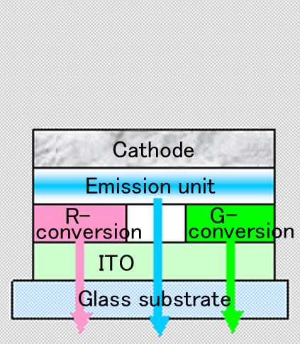
White OLED lighting devices are designed to achieve a white color by simultaneously
emitting light from organic substances that radiate in colors such as blue, red, and green. However,
changes in lighting colors due to aging (color shift) are inevitable because the durability of devices
differs from color to color. This is an issue that must be addressed in addition to the issue of
luminance lifetime. (A comparison of OLED device structures is shown in Figure 2.)
Superposition
Multi-unit (MPE) type Multi-layer emission type Color conversion type
(display method) type
In the case of “n” laminated Color shift after aging is less Capable of adjusting colors as
Capable of mixing colors with a
units, the luminance is significant but requires a costly with displays, but requires a
simple structure but has
increased nearly n-fold; at a color conversion layer and has complicated and expensive
problems delivering high
fixed luminance, the current is problems delivering high drive circuit and has problems
luminance.
reduced to 1/n. luminance. delivering high luminance.
Figure 2 Comparison of light-emitting device structures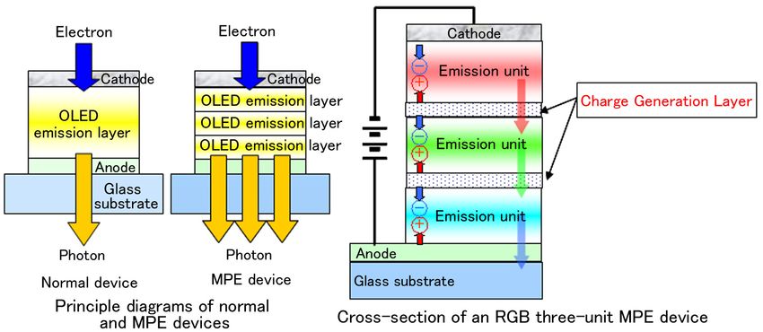
Mitsubishi Heavy Industries Technical Review Vol. 49 No. 1 (March 2012)
49
To cope with the color shift, we have tried to lengthen the lifetime of the blue devices, which
have the lowest durability. We discovered that the most essential factor is to maintain carrier
balance of electrons and holes over a long period of time. We succeeded in developing a stable
carrier transport structure that produced a blue device with a lifetime more than five times longer
than that of existing blue devices. This dramatically increased the color shift lifetime, and led us to
launch a panel product that performed at practical levels. (The specifications of the panel products
are shown in Table 1.)
Table 1 Performances of a standard panel
Type of color
Item Units
Warm white Natural white
Panel outer dimensions (W L t) mm 145 145 2.3
Panel weight g 107
Dimensions of emission area mm 125 125 (150 cm2)
Total luminous flux lm 99 99
Rated current A 0.9 0.9
Rated voltage V 10.7 10.5
Luminous efficacy lm/W 10.3 10.5
Color temperature K 2 , 800 4 , 900
General color rendering index Ra 82 81
Chromaticity coordinates (x, y) (0.45, 0.42) (0.35, 0.38)
Rated luminance cd/m2 2 , 800 2 , 700
h (1 , 000cd/m2) 50 , 000 100 , 000
Half-decay luminance lifetime
h (3 , 000cd/m2) 10 , 000 20 , 000
|3. Development of Light Out-Coupling Technology
In an OLED device structure, multiple organic layers are vacuum-deposited on a glass
substrate on which a transparent electrode (ITO**3) film is formed, and a metal layer is deposited as
a cathode. The outgoing light from the emission layer of the organic layers propagates in all
directions, and is emitted to outside from the glass substrate along with light reflected on the
cathode. However, the light that is totally reflected on the boundaries between the glass and ITO
and between the glass and external air layer is not emitted. Instead it remains inside and attenuates
due to differences in the refractive index. Thus, the actual amount of out-coupled light is only about
20% of the total light emission. To effectively extract light in the substrate mode, Lumiotec jointly
developed a light out-coupling film (a resin film with a prism lens formed on the surface) with its
parent company, Toppan Printing. The film was attached on the surface of the glass substrate to
reduce the reflectance on the boundary between the glass and external air layer, thereby improving
the light out-coupling efficiency (up to 1.5 times). (Figure 3 shows the light propagation mode of
OLED devices and the effects of the light out-coupling film.)
**3: Abbreviation for indium tin oxide.
The light out-coupling film was obtained by integrating optical design technology owned by
Toppan Printing with other microfabrication techniques. We plan to further improve the light
out-coupling efficiency in tandem with the optical design of OLED devices, and collaborate in the
development of a new light out-coupling structure technology targeting the loss reduction of the
thin-film mode.
Figure 3 Light propagation mode of OLED devices and effects of the light out-coupling film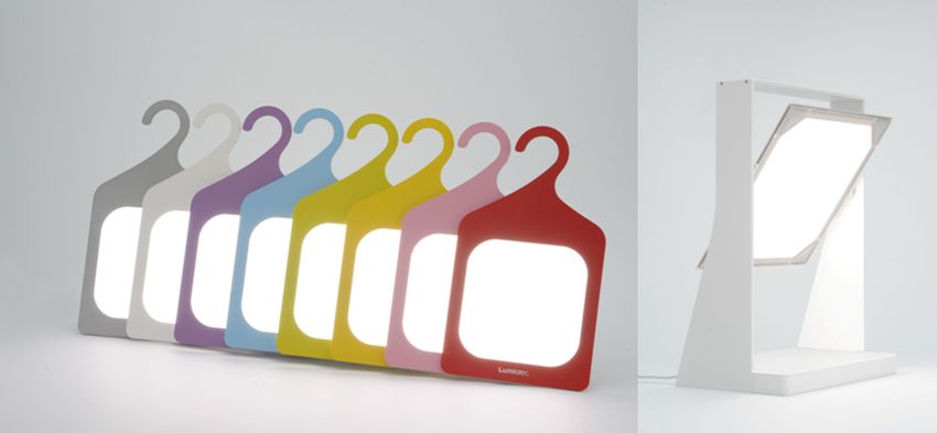
Mitsubishi Heavy Industries Technical Review Vol. 49 No. 1 (March 2012)
                                                                                                         50

|4. Development of Encapsulation Technology
4.1    Encapsulation technology for OLED lighting
       To prevent degradation of OLED devices, the substrate on which the devices are formed
needs to be encapsulated with a glass cap or other means. In OLED displays, devices are normally
encapsulated by filling gas such as nitrogen, but this type of encapsulation suffers from poor heat
conductivity and thus cannot withstand high-power input for lighting applications. If turned on at a
high luminance, the device would be overheated due to insufficient heat dissipation around the
power-feeding terminal and, at worst, damaged by thermal runaway. Thus far, fluorine-based or
other types of insulating oil have been used for encapsulation to improve the heat dissipation to a
certain degree, but the method is less productive and has limitations.
4.2    New encapsulation technology
       While addressing these problems, we also strived to provide encapsulation using a common
less-costly plate glass substrate, instead of an expensive cavity cap, and developed a gel
encapsulation process. Gel is a material that has properties between solid and liquid. It is easier to
handle than liquid. In addition, gel-based encapsulation does not require stringent considerations
for impacts on the OLED device or an expensive vacuum process, unlike solid encapsulation. We
have developed a mass-production process that uses techniques such as dispensing, printing, and
bonding, which are commonly used in manufacturing processes of flat panel displays.
       We selected a gel material that does not cause device deterioration, and dispersed an
inorganic desiccant in the gel instead of using desiccant attached to a cap. Consequently, the heat
conductivity and heat dissipation were both improved. In addition, we achieved an encapsulation
performance comparable to that of the existing process, while at the same time reducing the panel
thickness to 2.3mm.
       As a result, when comparing 142-mm square panels at 5,000 cd/m2, the panel temperature
                                      o
was reduced by approximately 12 C at maximum (Figure 4). This improved the lifetime and
reliability of the panel, making it possible to provide practical OLED lighting panels.

  Figure 4   Emission state of panel and heat generation (when lighting at 5,000 cd/m2)

|5. Development of Mass-Production Technology
5.1    Overview of the in-line deposition system
      For the film formation equipment, which is the most crucial aspect in the manufacturing
process, we use an in-line deposition system with linear evaporation sources developed by MHI
(Industrial Machinery Business, Technology & Solutions Division) exclusively for manufacturing
for OLED lighting panels. (An overview of this system is shown in Figure 5.) The system consists
of a vacuum chamber, linear evaporation sources, a substrate carrier, and a vacuum pumping
system. The linear evaporation sources are long-length crucibles that evaporate organic materials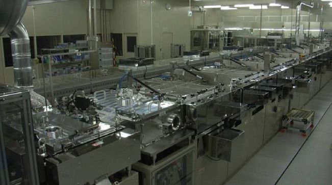
Mitsubishi Heavy Industries Technical Review Vol. 49 No. 1 (March 2012)
51
into a linear form. They are arranged in the vacuum chamber at predetermined intervals according
to the number of organic film layers. By continuously conveying glass substrates placed on trays
above the linear evaporation sources with only a small gap between the adjacent trays, organic
materials are laminated to form a lamination film on the lower side of each substrate (Figure 6).
The process is suitable for low-cost mass-production of OLED lighting panels because it features a
highly efficient use of expensive organic materials and a shorter tact time enabled by continuous
conveyance.
Figure 5 Overview of the in-line Figure 6 Schematic diagram of linear evaporation
deposition system sources and in-line conveyance
5.2 Operation results
The in-line deposition system was installed in Lumiotec's Yonezawa Plant in August 2009.
Thus far, the system has been operated at full capacity for production and development for more
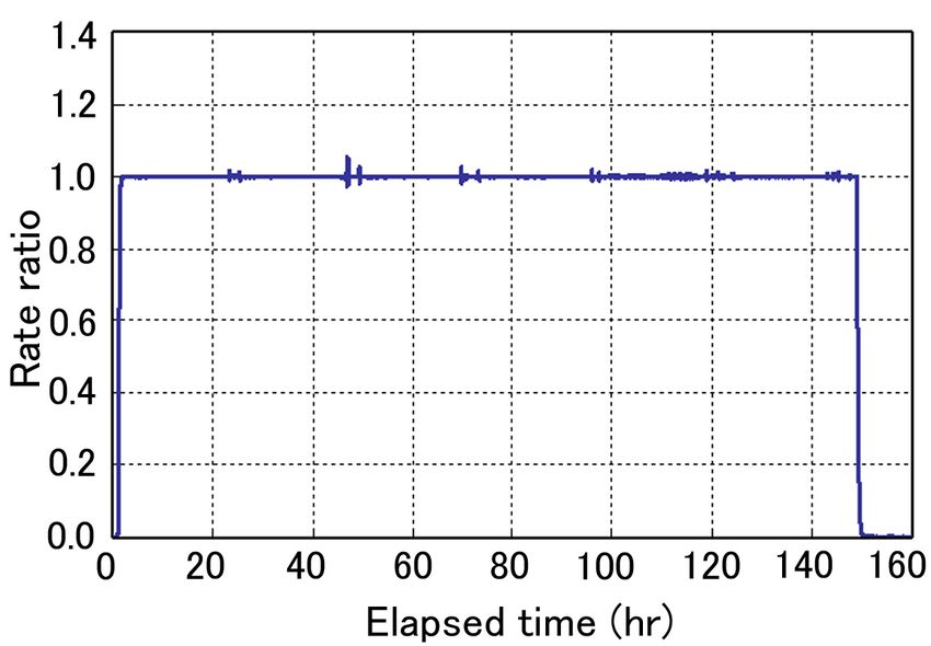
than two years. The system has achieved an in-plane film thickness distribution within ±2%
(Figure 7), and a long-term deposition rate stability within ±2% for 144-hour continuous operation
(Figure 8). The in-plane film thickness distribution is an essential factor for producing high-quality
panels, while the long-term deposition rate stability is necessary to improve the yield. The system
is contributing to the production of panels with stable quality.
Using the system, the company started manufacturing and selling a total of 10 models in
January 2011. They are available in five shapes (square in two sizes, large and small; and rectangle
in three sizes, large, medium, and small), each model in two lighting colors (warm white and
natural white). (See the photo at the top of the article.) Different panel shapes are provided by
changing the deposition masks, and various lighting colors of the panels are produced merely by
changing some of the light-emitting materials. In this way, production of multiple models can be
efficiently realized with only a single deposition system.
Figure 7 In-plane film thickness distribution Figure 8 Long-term stability of film
deposition rate
|6. Development of a Next-Generation Panel
6.1 Latest development status (goals and results)
All the panels launched at the end of fiscal year 2010 used fluorescent materials. However,
phosphorescent materials will be used in our next-generation panels, which are slated for launch in
spring 2012. The use of phosphorescent materials provided by Universal Display Corporation is an
essential technique for improving efficiency, because theoretically they can enhance the internal
luminous efficiency by up to 100% (four times as high as that of fluorescent materials). In general,
approximately 80% of the light generated in a device is lost in the panel. Thus, “light out-coupling
technology” to extract the light otherwise lost will be a key point for development in the future.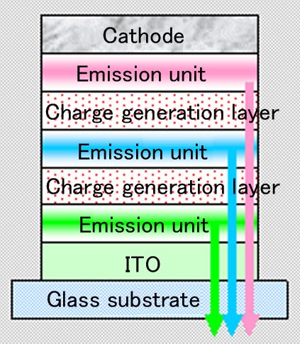
Mitsubishi Heavy Industries Technical Review Vol. 49 No. 1 (March 2012)
52
With the synergistic effect of these new technologies, our new device achieved a luminous
efficacy of 40 lm/W and demonstrated the ability to deliver high-efficiency, high-luminance, and a
long-lifetime simultaneously. (The performance specifications of the new OLED lighting panels
are shown in Table 2.)
Table 2 Target performances of next-generation panels
Type of color temperature
Item Units
Warm white White
Panel outer dimensions (W L t)mm 145 145 2.3
Panel weight g 107
Dimensions of emission area mm 125 125 (156 cm2) without square electrode
Total luminous flux lm 110 110
Rated current A 0.36 0.49
Rated voltage V 7.5 9.0
Luminous efficacy lm/W 40.0 25.0
Color temperature K 3,000 4,000
General color rendering index Ra 79 83
Chromaticity coordinates (x, y) (0.43, 0.42) (0.38, 0.38)
Rated luminance cd/m2 3,000 3,000
h (1,000cd/m2) 60,000 125,000
Half-decay luminance lifetime
h (3,000cd/m2) 12,000 25,000
6.2 Structure and features of the devices
The new panels incorporate a high-efficiency white MPE device featuring a light
out-coupling efficiency that has been significantly improved by our proprietary internal optical path
design technique. As a result, the product achieved performances that meet market efficiency
requirements. The improved efficiency also has a variety of secondary effects, such as reduced heat
o
generated in the lighting panel (36 C at room temperature), and reduced component costs. We have
already developed a high-color temperature model (4,000 K/white) with an efficiency of 25 lm/W,
but we plan to aim for higher efficiency in fiscal year 2012.
In the development of new panels, we focused on the issues that have arisen in relation to the
existing panels, such as improved luminous efficacy and reduced angular dependence of colors.
Because we cannot expect sufficient effects simply by improving the internal luminous efficiency
with the use of a phosphorescent emission mechanism, the device structure was entirely revamped
to facilitate stable mass-production, low-voltage drive, and out-coupling of light. Furthermore, we
adopted a technique for optimizing the optical design to obtain the maximum out-coupling
efficiency and uniform angular distribution of wavelengths during the out-coupling film attachment
process. With the combined effects of new technologies, we achieved the highest luminous efficacy
and longest lifetime for the existing materials, as well as an excellent angular distribution of
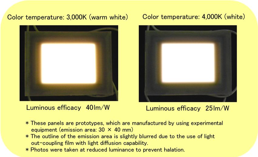
luminous intensity (Figure 9: photo of 30 × 40-mm prototype panels).
The panels incorporate UniversalPHOLED® phosphorescent OLED technology and materials from
Universal Display Corporation.
Figure 9 Light emission of new panels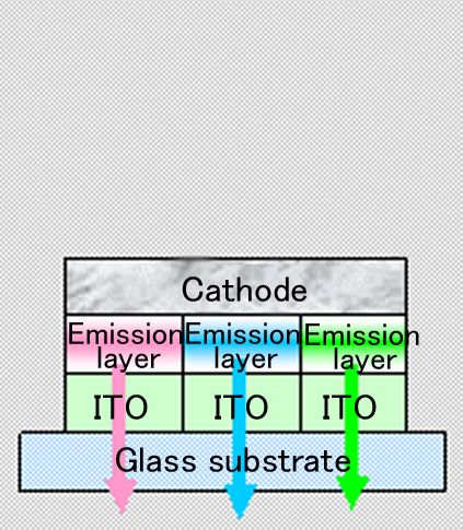
Mitsubishi Heavy Industries Technical Review Vol. 49 No. 1 (March 2012)
                                                                                                                 53

|7. Conclusion
      We started selling two types of design luminaires with our OLED lighting panels in
September 2011 (Figure 10: portable “HANGER” and desktop “VANITY”). The products were
exhibited and well received at one of the largest international furniture trade fairs in the world
(Milano Salone) held in Milan, Italy, in March 2011. These are the world’s first commercially
available luminaires to incorporate a mass-produced OLED lighting panel and a dedicated compact
driver module. By developing high-efficiency panels using phosphorescent materials, we will strive
to improve further various performance characteristics such as luminous efficacy and to reduce
production costs. Through these efforts, we will try to promote the widespread use and
commercialization of OLED lighting panels, so that we can make contributions to improving the
global environment.

  Figure 10   Lumiotec's design luminaires “Hanger” in eight colors and “Vanity”

  References
   1.   Ogasawara et al., Development of Production System of OLED Panel for Lighting Purpose, Mitsubishi
        Juko Giho Vol. 46 No. 1 (2009) pp. 33-35
   2.   Organic Light-Emitting Diode Panels for Lighting, Mitsubishi Heavy Industries Technical Review Vol. 47
        No. 1 (2010) pp.51-52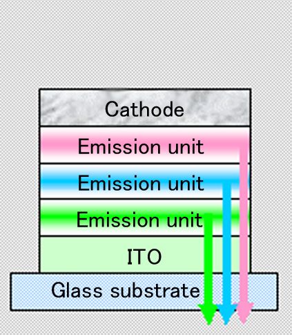
You can also read