Define and measure the dimensional accuracy of two-photon laser lithography based on its instrument transfer function
←
→
Page content transcription
If your browser does not render page correctly, please read the page content below
PAPER • OPEN ACCESS

Define and measure the dimensional accuracy of two-photon laser
lithography based on its instrument transfer function
To cite this article: Gaoliang Dai et al 2021 J. Phys. Photonics 3 034002

View the article online for updates and enhancements.

                                This content was downloaded from IP address 46.4.80.155 on 22/09/2021 at 09:40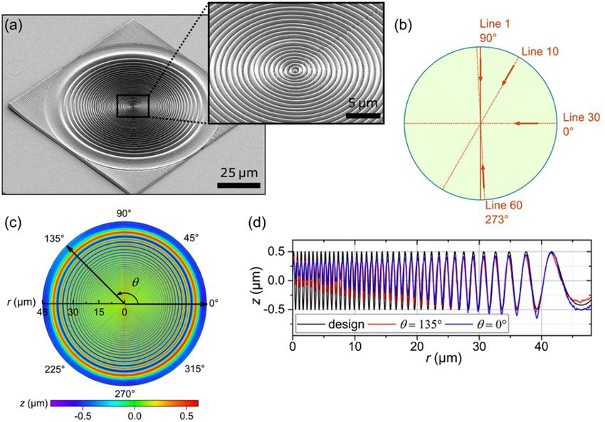
J. Phys. Photonics 3 (2021) 034002 https://doi.org/10.1088/2515-7647/abfaa7
Journal of Physics: Photonics
PAPER
Define and measure the dimensional accuracy of two-photon
OPEN ACCESS
laser lithography based on its instrument transfer function
RECEIVED
18 December 2020 Gaoliang Dai1,∗, Xiukun Hu1, Julian Hering2,3, Matthias Eifler2,4, Jörg Seewig4
REVISED
10 March 2021
and Georg von Freymann3,5
1
ACCEPTED FOR PUBLICATION Physikalisch-Technische Bundesanstalt, 38116 Braunschweig, Germany
2
9 April 2021 Opti-Cal GmbH, 67663 Kaiserslautern, Germany
3
PUBLISHED
Department of Physics and Research Center OPTIMAS, Technische Universität Kaiserslautern, 67663 Kaiserslautern, Germany
4
11 May 2021 Lehrstuhl für Messtechnik & Sensorik, Technische Universität Kaiserslautern, 67663 Kaiserslautern, Germany
5
Fraunhofer Institute for Industrial Mathematics ITWM, 67663 Kaiserslautern, Germany
∗
Author to whom any correspondence should be addressed.
Original content from
this work may be used E-mail: gaoliang.dai@ptb.de
under the terms of the
Creative Commons Keywords: two-photon polymerization (TPP), direct laser writing (DLW), 3D micro- and nanomanufacturing, dimensional accuracy,
Attribution 4.0 licence.
instrument transfer function (ITF), atomic force microscopy
Any further distribution
of this work must
maintain attribution to
the author(s) and the title
of the work, journal
Abstract
citation and DOI. Two-photon polymerization (TPP) is a powerful technique for direct three-dimensional (3D)
micro- and nanomanufacturing owing to its unique ability of writing almost arbitrary structures of
various materials. In this paper, a novel method is proposed to quantitatively define and measure
the dimensional accuracy of TPP tools based on the concept of instrument transfer function (ITF).
A circular linear-chirp pattern is designed for characterizing the ITF. Such a pattern is arranged in a
linear chirp function with respect to its radial distance r from the pattern centre, thus, well
representing a signal with a quasi-flat amplitude over a given spectral bandwidth. In addition, the
pattern is rotational symmetric, therefore, it is well suited for characterizing the ITF in different
angular directions to detect angular-dependent asymmetries. The feasibility of the proposed
method is demonstrated on a commercial TPP tool. The manufactured pattern is calibrated by a
metrological large range atomic force microscope (AFM) using a super sharp AFM tip, thus the
dimensional accuracy and angular-dependent anisotropy of the TPP tool have been well
characterized quantitatively. The proposed method is easy to use and reveals the dimensional
accuracy of TPP tools under real manufacturing conditions, which concerns not only the optical
focus spot size of the exposing laser but also influencing factors such as material shrinkage,
light–matter interaction and process parameters.
1. Introduction
Two-photon polymerization (TPP) [1] is a powerful three-dimensional (3D) micro- and nanofabrication
technique based on nonlinear light–matter interaction. In TPP processing, femtosecond laser pulses are
focused into a photosensitive material, where two-photon absorption [2] and subsequent polymerization in
an extremely localized focal volume (voxel) is induced. By scanning the laser focus with respect to the
photoresist, e.g. by a galvanometric mirror scanner, TPP allows for ultra-fast structuring in a layer-by-layer
process. Due to its flexibility and high resolution while reaching feature sizes into the sub-100 nm region [3],
TPP enables research in many fields, e.g. photonic crystals [4, 5], topological insulators [6, 7], biological
cell-scaffolds [8–10], photonic and mechanical metamaterials [11, 12], as well as industrial relevant
applications, like micro-optical elements [13–16], and material measures [17–19].
Resolution and writing speed (i.e. the manufacturing throughput) have been tremendously improved in
recent years. However, an objective comparison between different TPP devices or different materials with
respect to structural quality and fabrication yield is still difficult. With increasing industrial applications,
such a comparison is highly sought after, as it supports the decision which type of material might yield the
© 2021 The Author(s). Published by IOP Publishing Ltd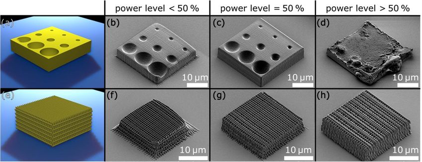
J. Phys. Photonics 3 (2021) 034002                                                                       G Dai et al

best results on a certain type of TPP device. Furthermore, it might support the development of smart
algorithms, which automatically optimize the writing strategies for arbitrary structures. So far, structures are
optimized following a trial-and-error route, based on the experience of the user. For most of the structures,
going to the physical limits of the device and material is often not necessary. For example, for the application
of printing highly accurate micro-lenses using stimulated emission depletion (STED) inspired TPP [20], the
dimensional accuracy is the more important quality criteria than resolution. However, resolution is the
quantity which is most often found in literature to define the performance of TPP. Although TPP resolution
has been rapidly improved in the past decade [20–23], resolution alone tells nothing about the overall
structural quality reached. Furthermore, resolution is often confused with feature size, for which the lateral
and/or axial size of a single voxel is typically applied [1]. A single voxel might be measured using, e.g. the
ascending scan method [24, 25] or the suspending bridge method [23]. The measurement of the voxel shape
may suffer from the so-called truncation effect [24], impacting the measurement accuracy. Furthermore, the
feature size does not reveal the true resolving capability of a TPP tool, because the resolution of a TPP
process depends not only on the focal spot size of the laser, but also on the nonlinear interaction of
light-matter, the material’s shrinkage, diffusion, deformation of the structure as well as the process
parameters (e.g. the distance between two adjacent lines during fabrication, the writing speed, etc). To
measure resolution, the accepted way is to measure the distance between two lines or more generally two
features, which can be done either laterally or axially. While lateral resolution down to 120 nm [22] has been
demonstrated along these lines using STED-inspired TPP, this again does not tell too much about the
fabrication capability of complex structures, as the writing process of adjacent features can be strongly
affected due to the consumption of photoinitiators and diffusion of various species (photoinitiators,
scavengers) [26]. Fischer et al suggested to fabricate a 3D periodic unit, e.g. a woodpile photonic crystal for
determining both axial and lateral resolution of a given photopolymerizable system [20]. While it is
advantageous for characterizing the lateral and axial resolution of the tool simultaneously, it needs either a
relatively complex spectral evaluation route, which only indirectly measures the resolution or it requires a
combination of focussed ion beam (FIB) slicing and electron beam microscopy to retrieve the parameters.
     In this paper, we propose a novel method for quantitatively characterizing the dimensional accuracy of a
TPP tool and the used material based on its instrument transfer function (ITF). For characterization, an
atomic force microscope (AFM) is sufficient, which does not have to reach atomic resolution and allows for
characterization at much lower cost than FIB/electron-beam or spectral characterization. The ITF generally
describes the response of a system in terms of the frequency components between its input and output
signals and has been investigated in the field of optical microscopy [27]. In a TPP process, such an ‘input
signal’ represents the designed 3D model of a structure applied to a TPP tool for printing, while the ‘output
signal’ is the manufactured 3D structure. In such a way, the ITF can be understood as the printing capability
of a TPP tool as a function of the object’s spatial frequency components. This concept has the advantage that
it is consistent with the ISO standardization in the geometrical product specification, namely the ISO 25178
parts 600 [28] and 70 [29], defining the material measures and metrological characteristics for, e.g. the
resolution of optical areal surface topography measuring instruments based on their ‘topography fidelity’.

2. Method

To test the dimensional accuracy of TPP tools, we design a circular linear-chirp pattern. Two main ideas are
implemented in this design. First, sample features are arranged in a linear chirp function with respect to its
radial distance r from the pattern center. Such a linear chirp function profile represents a 3D surface
topography with a quasi-flat amplitude over a given bandwidth, which is preferable for characterizing the
ITF. Second, the pattern is rotationally symmetric, thus it is ideal to evaluate angular-dependent asymmetries
of TPP tools by characterizing the ITF features in different angular directions. This radial arrangement tests
the scanning axis of the TPP tool, as well as certain asymmetries introduced by aberrations/polarization.
While the chirp directly tests the achievable dimensional accuracy in lateral direction, the request for
constant surface modulation tests the dimensional accuracy in axial direction as well as the power dependent
cross-linking density.
    Mathematically, a linear chirp function can be described as
                                                    (        (          ))
                                               H                   ∆f
                                     z (r) =     sin Φ0 + 2πr f0 −    r    ,                                    (1)
                                               2                   2R

where H is the feature height; the pattern has a linearly changing spatial frequency with respect to r, i.e.
                                                                                     topo
f (r) = f0 − Rr ∆f; R is the radius of the outermost borders of the pattern; f0 = 1/λmin is the initial topographic
frequency; and ∆f is the bandwidth of the structure

                                                2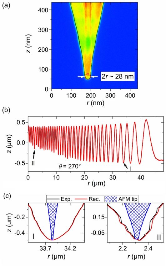
J. Phys. Photonics 3 (2021) 034002 G Dai et al
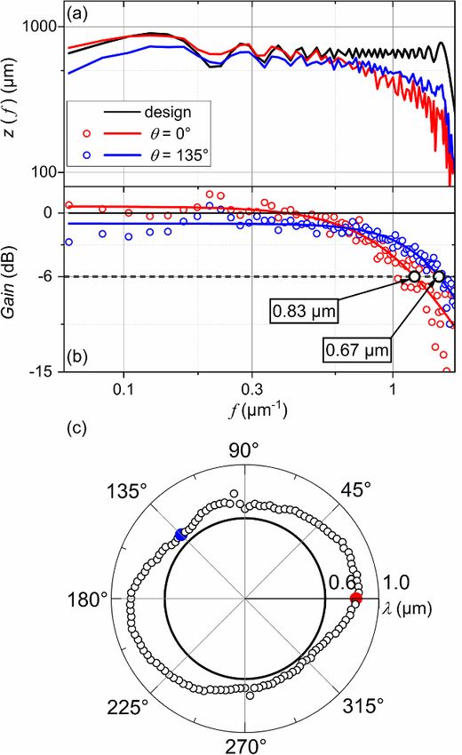
Figure 1. (a) SEM images of a chirped pattern fabricated by TPP similar to the one measured in (c); (b) schematic diagram
showing the principle of the radial scanning strategy applied in measuring the pattern; (c) AFM image taken by the radial
scanning strategy shown as raw measurement data after 1st order levelling. Each radial profile is scanned with 48001 pixels and a
pixel distance of 2 nm; (d) radial profiles of θ = 0◦ (blue) and θ = 135◦ (red) at the marked positions in (c) and the design
profile (black).
/ /
∆f = 1 λtopo − 1 λtopo
max
, (2)
min
topo topo
where λmin denotes the minimum radial spatial wavelength and λmax denotes the maximum radial spatial
wavelength.
To get the accurate knowledge of the ‘output signal’ — the 3D geometry of the manufactured pattern,
exemplarily shown as SEM image in figure 1(a) — a 3D microscopic technique, which possesses better
resolution than the TPP tool has to be applied. A very suitable candidate tool for this purpose is AFM, which
is widely applied for characterization of various nanostructures with both a high lateral resolution (down to
a few nm determined by the AFM tip geometry) and a high vertical resolution (at sub-nm level). In this
study, we measure the manufactured pattern by a metrological large range AFM (Met. LR-AFM) developed
at the Physikalisch-Technische Bundesanstalt — the national metrology institute of Germany. The details of
this tool can be found elsewhere [30–33].
During AFM measurements, one has to consider the tip dilation effect. The image obtained by the AFM
is the dilated result of the measured feature with the tip shape [34], which will consequently bias the
spectrum of the calibrated data sets. To mitigate the tip dilation effect, super sharp AFM tips (SSS-NCLR,
NANOSENSORSTM ) are applied in this study.
The so-called radial scanning strategy used here is schematically illustrated in figure 1(b) and was first
designed for measuring rotation symmetrical structures, such as Rockwell indenters [35]. In measurements,
profiles are measured in a radial direction through the center of the pattern. The advantages of this
measurement strategy are two-fold. First, the measurement time can be reduced significantly, as the number
of needed measurement profiles can be reduced. Second, the pixel density along the radial profiles can be
increased without impacting the needed measurement time, thus enhancing the sampling frequency of the
reference data.
The TPP pattern is manufactured by a commercial TPP tool (Photonic Professional GT+, Nanoscribe
GmbH) equipped with a 63× objective lens with a nominal numerical aperture (NA) of 1.4 (Carl Zeiss
Microscopy GmbH) and with a galvanometric mirror scanner with a scan speed of 20 mm s−1 . The built-in
fibre laser is specified with a central wavelength of 780 nm, a repetition rate of 80 MHz and a pulse duration
3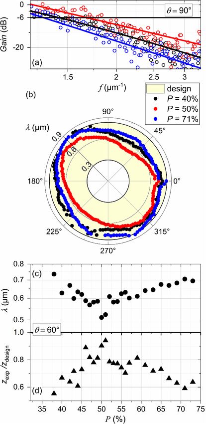
J. Phys. Photonics 3 (2021) 034002                                                                                           G Dai et al

   Figure 2. (a) SEM image of the SSS-NCLR AFM tip after being applied in AFM measurements. The contour of the tip is evaluated
   as the tip geometry, showing a tip radius of about 14 nm; (b) reconstructed result (red) of the measured profile (black) (θ = 270◦
   in figure 1) by the tip geometry determined in (a); (c) detailed zoomed-in views showing the raw profile (black), reconstructed
   profile (red) and the tip geometry (crosshatched blue) at the marked positions I and II.

of roughly 100 fs. All manufacturing processes have been performed in an air-conditioned room at 21 ◦ C and
J. Phys. Photonics 3 (2021) 034002                                                                                            G Dai et al

   Figure 3. (a) Amplitude curves calculated by Fourier transformation of the designed profile and two measured radial profiles
   along the angular direction of θ = 0◦ and θ = 135◦ ; (b) evaluated (open circles) and fitting (solid lines) ITF curves of the TPP
   tool along two angular directions; (c) evaluated dimensional accuracy along different angular directions, which is defined as the
   wavelength of the printed profile where the gain is dropped to −6 dB.

    Based on the aforementioned theory, the ITF of the TPP tool can be evaluated as
                                                           Fm (θ, f ) FFT {Vm (r, θ)}
                                           ITF (θ, f ) =              =                                                                (3)
                                                           Fd (θ, f )   FFT {Vd (r, θ)}
where, ITF (θ, f ) denotes the ITF in polar coordinates; Fm (θ, f ) and Fd (θ, f ) are the Fourier transformation
results of the measured profile Vm (r, θ) and the designed profile Vd (r, θ) in the orientation of θ in polar
coordinates.
    Figure 3(a) depicts the amplitude curves calculated by Fourier transformation of the designed profile and
the measured radial profiles along two angular directions of θ = 0◦ and θ = 135◦ shown in black, red and
blue, respectively. After applying equation (3), the ITF curves of the TPP tool along these two angular
directions can be calculated, as plotted in figure 3(b) (open circles). It can be seen that the ITF keeps almost
constant at low spatial frequencies. It indicates that the features, which have lower spatial frequencies than the
dimensional accuracy of the TPP tool can be well printed. However, the gain of the ITF curves starts to decay
when the spatial frequency is increased from 0.4 to 1.6 µm−1 , indicating the loss of printed features due to
reaching the dimensional accuracy limit of the TPP tool as well as feeling the influence of proximity and other
material related effects. Thus, the ITF curve can well represent the dimensional accuracy of the TPP tool.
    To achieve a better evaluation stability, we fit the evaluated ITF curve to the function:
                                                                       k
                                                      G(f) = [                n]                                                       (4)
                                                                  1 + (m · f )

where G denotes the gain and f denotes the spatial frequency; the parameter k is introduced to represent the
z-scaling factor; the parameters m and n are introduced to describe the bandwidth characteristics of the
instrument. The fitting curves are shown as solid lines in figure 3(b).
    To have a quantitative definition, we define the dimensional accuracy limit of the TPP tool as the value of
the wavelength where the gain of the ITF curves drops to −6 dB, as shown in figure 3(b). At this wavelength,

                                                       5
J. Phys. Photonics 3 (2021) 034002 G Dai et al
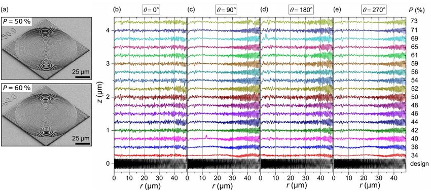
Figure 4. (a) Exemplary SEM images of the circular chirp pattern fabricated with P = 50% and P = 60% of the maximal laser
power similar to the ones measured in (b)–(e); (b)–(e) measured radial profiles (vertically offset for clarity) of the patterns
printed with different power levels ranging from 34% to 73% of its maximal power. The profiles are extracted along the angular
direction θ of (b) 0◦ , (c) 90◦ , (d) 180◦ , (e) 270◦ , respectively.
the amplitude of the printable feature drops at the half of the designed amplitude. For the example shown in
the figure 3(b), the dimensional accuracy limit is evaluated as 0.83 and 0.67 µm for the two angular
directions of θ = 0◦ and θ = 135◦ , respectively. After calculating the ITF and its corresponding dimensional
accuracy at all angular directions ranging from θ = 0◦ to θ = 360◦ as mentioned above, we obtain the
angular-dependent dimensional accuracy of the tool, as plotted in figure 3(c). It has rather a quasi-elliptical
shape than a circular shape, which may be owing to the optical aberrations of the microscopic set up. Besides,
a non-perfect circular polarisation of the excitation laser beam distorts the theoretical round shape of the
focus within the xy-plane, thus resulting in additional asymmetries regarding the lateral dimensional
accuracy. Another reason can be assumed by the unidirectional fabrication of the structure along the angular
direction of θ = 90◦ (hatching direction). This was carried out to avoid angular-direction-dependent
non-synchronizations of laser power ramping and galvo-mirror positioning during the polymerization
process, which was found in previous experiments.
One may wonder why the dimensional accuracy value evaluated in our proposed method is much larger
than, e.g. the diffraction limit of the applied optical microscope (λ/(2 NA) = 0.278 µm) or higher
resolutions reported with these commercial devices. But having in mind the complex interplay of optics and
materials in TPP, these differences do not surprise at all. The very best resolution results for two separated
lines are a very special case with not too much relation to actual structures printed. Along these lines it is
reassuring that the practical specifications given for the used TPP device are close to the values found by the
proposed method. Therefore, the proposed method can indeed provide a quantitative measure for the
dimensional accuracy reachable for an actual structure under certain fabrication conditions and not only the
physical limitation based on optical diffraction effects.
3. Application
The ITF method introduced above has advantages of characterizing the dimensional accuracy of TPP
manufacturing including the contributions not only from the optics, but also from the light–matter
interaction and the printing process. Furthermore, the method can be well applied to investigate the influence
of process parameters on the dimensional accuracy of TPP tools. For instance, by printing the test patterns
with varied process parameters, the dependency of the dimensional accuracy on the process parameters can
be obtained, which could thus offer a basis for the process optimization. In general, this will speed up the
process for structure optimization as a very good set of starting parameters can be easily determined. Of
course, this will not yet replace optimization in detail, if one wants to work at the physical limits of the tool.
To demonstrate such an application, in this study we investigate the impact of laser power on the
topo
dimensional accuracy. We designed another pattern with a wavelength range of λmin = 0.3 µm to
topo
λmax = 0.9 µm, a feature height of H = 300 nm and a radius of the outermost borders of the pattern of
R = 50 µm. A number of patterns are printed with varying pre-defined power levels, ranging from 34% to
73% of the maximal laser power (Pmax ∼50 mW at the entrance pupil of the objective). This generalized
6J. Phys. Photonics 3 (2021) 034002 G Dai et al
Figure 5. (a) Evaluated (open circles) and fitting (solid lines) ITF curves of the TPP tool along θ = 90◦ at three power levels P of
40% (black), 50% (red) and 71% (blue), respectively; (b) evaluated printing dimensional accuracy values along different angular
directions for three different power levels P of 40% (black), 50% (red) and 71% (blue), respectively; (c) dependence of evaluated
printing dimensional accuracy values on the power level at θ = 60◦ ; (c) height ratio of the printed profile (zexp ) to the design
value (zdesign ) at λtopo = 0.83 µm which corresponds to the last peak position of the designed curve in figure 4.
power level is set by multiplication of two variables: the so-called ‘power scaling’ and ‘laser power’. While the
power scaling variable has to be fixed for the complete structure, the laser power variable can be adjusted
spatially within the designed pattern to achieve, e.g. an equal exposure dose at all printing positions. This was
used to realize an overall constant height of the chirp’s amplitudes. Exemplary SEM images of sputter coated
patterns fabricated with 50% and 60% of the maximal laser power are shown in figure 4(a). The radial
profiles of many un-sputtered patterns printed with varying power levels measured by AFM are compared in
figures 4(b)–(e) along the angular direction θ of 0◦ , 90◦ , 180◦ , 270◦ , respectively. The designed radial profile
is shown at the bottom of figures 4(b)–(e). As can be seen in figure 4(c), the amplitude of the printed features
reduces significantly when the spatial frequency of the signal increases, indicating that the tool cannot well
print the designed structures at higher spatial frequency due to the limit of its dimensional accuracy. In
addition, the printed profiles show different behaviour at different power levels. For instance, the amplitudes
of the printed features increase when the power level is increased from 34% to 50% and then decrease for
higher power levels of 52% to 73%. It indicates the impact of the laser intensity on the dimensional accuracy
of the TPP. At first sight this seems anti-intuitive, since higher power levels are expected to worsen the
resolution, due to the increasing voxel size and proximity effect. Of course, increasing the overall laser
intensity is not what is usually done for reaching the highest resolution. But for dimensional accuracy, this is
exactly the expected behaviour. Too low power levels result in low cross-linking density and, hence, in
reduced structural stability, so that well defined features are not possible to reach. This behaviour is well
7J. Phys. Photonics 3 (2021) 034002 G Dai et al
Figure 6. (a) Illustration of the target bowl-containing structure; (b)–(d) scanning electron microscopic images of the
corresponding fabricated structures with power levels below, equal and greater than 50%; (e) illustration of the target woodpile
structure with rod distances of 0.8 µm; (f)–(h) scanning electron microscopic images of the corresponding fabricated structures
with power levels below, equal and greater than 50%.
represented in the ITF evaluation as shown in figure 5(a), where the evaluated ITF curves (open circles)
together with the fitting curves (solid lines) along θ = 90◦ of three selected power levels P of 40%, 50% and
71% are plotted in black, red and blue, respectively. The curves indicate that the conformity of the structure’s
amplitude is of great importance. For low power levels, e.g. P = 40%, this amplitude is getting lower, too.
Consequently, the −6 dB drop is already reached at low topographic frequencies (∼1.4 µm−1 ), leading to the
observed worsened dimensional accuracy value. On the other side, for considerable higher power levels, e.g.
P = 71%, the voxel size, proximity effect, etc become the limiting factors. In the end, the optimal power level
appears to be about 50% in this experimental scenario.
Furthermore, the printed profiles shown in figure 4 are also angular dependent. For instance, the
amplitude of the printed signal at θ = 0◦ is significantly smaller than that of other angular directions. The
reason can be found in the way of fabrication: in contrast to the example shown in section 2, the patterns
now are manufactured by circular movements of the laser focus around the center with increasing r, starting
at θ = 0◦ and ending at θ = 359◦ , respectively. Thereby, we expect an overall improvement in dimensional
accuracy, because there are way less power ramping procedures during such a ‘hatching circle’, thus, leading
to less fabrication errors, compared to a hatching line along the angular direciton of θ = 90◦ . As a
disadvantage, around θ = 0◦ , these non-perfect adaptions of the laser focus’ acceleration/deceleration with
regard to the required power level lead to the observable stronger deviation of the structure’s amplitude
around this angle. The angular dependence of the evaluated printing dimensional accuracy of the patterns
are shown in figure 5(b). For sake of clarity, again, only the results of patterns printed at three power levels P
of 40%, 50% and 71% are shown in black, red and blue, respectively. It can be seen from figure 5(b) that the
dimensional accuracy of the three patterns has a similar quasi-elliptical shape. The printing process achieves
the best result near θ = 45◦ while it has the worst dimensional accuracy near θ = 135◦ . Since the elliptical
shape is flipped with regard to the results in section 2 (see figure 3(c)), we can neglect the impact of the laser
focus’ non-symmetrical shape and optical aberrations, as they did not change at all. Instead, the way of
hatching and the resulting diffusion of photoinitiator and scavenger molecules, hence, the proximity effect,
seem to be generally much more critical for the fabrication results. Further optimizing the way of hatching
can possibly move this elliptical shape towards a circle and can be investigated in future research.
Figure 5(c) depicts the dependence of evaluated dimensional accuracy (along θ = 60◦ ) with respect to the
power level. It can be clearly seen that the TPP tool achieves the best dimensional accuracy of about 0.51 µm
at the power level of 50%. In addition, to show the dependence of the printed feature height on the power
level, the height ratio of the printed profile (zexp ) to the design value (zdesign ) is plotted in figure 5(d). It can
be seen that the printed structure reaches the highest amplitude also near the power level of 50%. Both plots
show excellent agreement with the expected tendency of the overall materials response, as mentioned above.
These values should now give a rough guideline for the fabrication of any other structures: a power level of
about 50% is expected to give a good conformity of the targeted and fabricated structues. Indeed, this can be
found experimentally as shown by a bowl-containing structure, illustrated in figures 6(a)–(d). Too low power
levels (25%) lead to significantly unwanted deformations due to the weak crosslinking density, whereas too
high power levels (55%) already result in micro-explosions.
8J. Phys. Photonics 3 (2021) 034002 G Dai et al
Regarding the above determined dimensional accuracy limit of the TPP tool, one can conclude from the
long main axis of the resolution ellipse in figure 5(b), that, e.g. line distances of roughly 0.8 µm should be
resolvable. Therefore, we fabricated woodpile photonic crystals with a respective nominal rod distance of
0.8 µm as benchmarks. Here, we found again the best structure conformity at a power level of 50%, with
clearly distinguished rods (figures 6(e)–(h)). Low power levels (40%) result in dramatic shrinkage and
deformation of the woodpiles due to the aformentioned reasons, whereas too high power levels (75%) lead to
adhesion between neighboring rods. Thus, those woodpiles can not be considered as resolved structures any
more.
While the circular chirp structure does not spare the user the fine-optimization, it allows for a rough
prediction of critical fabrication parameters like the power level or the resolution limit of the 3D printing
devices in use and might help in chosing the right material/parameter combination as well as guide the
development of automatic optimization algorithms.
4. Conclusions
In summary, we have proposed and demonstrated a new approach for characterizing the dimensional
accuracy of TPP tools based on the concept of ITF, which is consistent to the ISO 25178 and has been
investigated to describe the transfer behaviour of optical surface topography measuring instruments. Using
this approach, a TPP tool under investigation is commanded to print circular linear-chirp patterns. The
manufactured patterns are then measured by, e.g. an AFM tool to get its real feature topography. Based on
the designed 3D model of the pattern which represents the ‘input signal’ and the measured topography
which represents the ‘output signal’, the ITF of the TPP tool can be evaluated as the ratio between the Fourier
transformation results of the input and output signals. In this study, the circular linear-chirp pattern is
designed as a ‘signal’ for two folds of reasons. First, a signal in a linear chirp function could well represent a
surface topography with a quasi-flat amplitude over a given bandwidth, which is preferable for characterizing
the ITF. Second, the pattern is rotationally symmetric, thus it is ideal to characterize the ITF features in
different angular directions for detecting angular-dependent asymmetries of TPP tools.
Compared to previous methods which characterize device resolution only, our method could reveal the
overall dimensional accuracy of the TPP tool, including the contributions not only from the optics, but also
from the light–matter interaction and the printing process. Furthermore, the method can be well applied to
investigate the influence of process parameters on the dimensional accuracy of TPP tools. For instance, by
printing the test patterns with varied process parameters, our method could thus offer a basis for the process
optimization. As an example, the proposed method is applied in investigating the impact of the general
power level of a TPP tool on its dimensional accuracy, showing promising results.
The proposed method so far presents a first step towards better comparability of different TPP devices by
an objective measurable criterion, which is achievable without using FIB cross sections or spectral analysis of
complex 3D structures. Furthermore, using AFM for mechanical load experiments could possibly allow to
extract even more information about the polymer network, e.g. the local cross-linking density. Here, further
investigations in the future will allow even better statements about the right fabrication parameters.
Data availability statement
The data that support the findings of this study are available upon reasonable request from the authors.
Acknowledgments
Funded by the Deutsche Forschungsgemeinschaft (DFG, German Research Foundation) — Project-ID
172116086 — SFB 926, and the EMPIR project 15SIB09 3DNano co-financed by the Participating States and
from the European Union’s Horizon 2020 research and innovation programme.
ORCID iDs
Gaoliang Dai https://orcid.org/0000-0002-1611-0074
Matthias Eifler https://orcid.org/0000-0001-6628-7284
Georg von Freymann https://orcid.org/0000-0003-2389-5532
9J. Phys. Photonics 3 (2021) 034002 G Dai et al
References
[1] Maruo S, Nakamura O and Kawata S 1997 Three-dimensional microfabrication with two-photon-absorbed photopolymerization
Opt. Lett. 22 132–4
[2] Denk W, Strickler J H and Webb W W 1990 Two-photon laser scanning fluorescence microscopy Science 248 73–6
[3] Kawata S, Sun H B, Tanaka T and Takada K 2001 Finer features for functional microdevices Nature 412 697–8
[4] Deubel M, von Freymann G, Wegener M, Pereira S, Busch K and Soukoulis C M 2004 Direct laser writing of three-dimensional
photonic-crystal templates for telecommunications Nat. Mater. 3 444–7
[5] Seet K, Mizeikis V, Matsuo S, Juodkazis S and Misawa H 2005 Three-dimensional spiral-architecture photonic crystals obtained by
direct laser writing Adv. Mater. 17 541–5
[6] Jörg C, Letscher F, Fleischhauer M and von Freymann G 2017 Dynamic defects in photonic Floquet topological insulators New
J. Phys. 19 083003
[7] Fedorova Z, Jörg C, Dauer C, Letscher F, Fleischhauer M, Eggert S, Linden S and von Freymann G 2019 Limits of topological
protection under local periodic driving Light Sci. Appl. 8 63
[8] Hohmann J K and von Freymann G 2014 Influence of direct laser written 3D topographies on proliferation and differentiation of
osteoblast-like cells: towards improved implant surfaces Adv. Funct. Mater. 24 6573–80
[9] Malinauskas M et al 2014 3D microporous scaffolds manufactured via combination of fused filament fabrication and direct laser
writing ablation Micromachines 5 839–58
[10] Selimis A, Mironov V and Farsari M 2015 Direct laser writing: principles and materials for scaffold 3D printing Microelectron. Eng.
132 83–9
[11] Frenzel T, Kadic M and Wegener M 2017 Three-dimensional mechanical metamaterials with a twist Science 358 1072–4
[12] Qu J, Kadic M and Wegener M 2018 Three-dimensional poroelastic metamaterials with extremely negative or positive effective
static volume compressibility Extremes Mech. Lett. 22 165–71
[13] Žukauskas A, Malinauskas M, Reinhardt C, Chichkov B N and Gadonas R 2012 Closely packed hexagonal conical microlens array
fabricated by direct laser photopolymerization Appl. Opt. 51 4995–5003
[14] Gissibl T, Thiele S, Herkommer A and Giessen H 2016 Two-photon direct laser writing of ultracompact multi-lens objectives Nat.
Photon. 10 554–60
[15] Stender B, Mantei W and Houbertz R 2017 From lab to fab—high-precision 3D printing Laser Tech. J. 14 20–3
[16] Thiele S, Arzenbacher K, Gissibl T, Giessen H and Herkommer A M 2017 3D-printed eagle eye: compound microlens system for
foveated imaging Sci. Adv. 3 e1602655
[17] Hering J, Eifler M, Hofherr L, Ziegler C, Seewig J and von Freymann G 2018 Two-photon laser lithography in optical metrology
Proc. SPIE 10544 1054412
[18] Eifler M, Hering J, von Freymann G and Seewig J 2018 Manufacturing of the ISO 25178–70 material measures with direct laser
writing: a feasibility study Surf. Topogr. Metrol. Prop. 6 024010
[19] Eifler M, Hering J, von Freymann G and Seewig J 2018 Calibration sample for arbitrary metrological characteristics of optical
topography measuring instruments Opt. Express 26 16609–23
[20] Fischer J and Wegener M 2012 Three-dimensional optical laser lithography beyond the diffraction limit Laser Photonics Rev.
7 22–44
[21] Spangenberg A, Hobeika N, Stehlin F, Malval J P, Wieder F, Prabhakaran P, Baldeck P and Soppera O 2013 Recent advances in
two-photon stereolithography Updates in Advanced Lithography ed H Hosaka (London: IntechOpen) (https://doi.org/
10.5772/56165)
[22] Wollhofen R, Katzmann J, Hrelescu C, Jacak J and Klar T A 2013 120 nm resolution and 55 nm structure size in STED-lithography
Opt. Express 21 10831–40
[23] Devoe R J, Kalweit H W, Leatherdale C A and Williams T R 2003 Voxel shapes in two-photon microfabrication Proc. SPIE
4797 310–6
[24] Sun H B, Tanaka T and Kawata S 2002 Three-dimensional focal spots related to two-photon excitation Appl. Phys. Lett. 80 3673–5
[25] Hering J, Waller E H and Von Freymann G 2016 Automated aberration correction of arbitrary laser modes in high numerical
aperture systems Opt. Express 24 28500–8
[26] Waller E H and Von Freymann G 2016 Spatio-temporal proximity characteristics in 3D µ-printing via multi-photon-absorption
Polymers 8 297
[27] De Groot P and De Lega X C 2006 Interpreting interferometric height measurements using the instrument transfer function Fringe
2005 ed W Osten (Berlin: Springer) 30–7
[28] DIN EN ISO 25178–600 2017 Geometrical product specifications (GPS)—surface texture: areal—part 600: metrological
characteristics for areal-topography measuring methods (Berlin: Beuth Verlag)
[29] DIN EN ISO 25178–70 2017 Geometrical product specification (GPS)—surface texture: areal—part 70: material measures(Berlin:
Beuth Verlag)
[30] Dai G, Wolff H, Pohlenz F and Danzebrink H U 2009 A metrological large range atomic force microscope with improved
performance Rev. Sci. Instrum. 80 043702
[31] Jäger E, Manske E, Hausotte T and Büchner H J 2000 Nano measuring machine for zero Abbe offset coordinate-measuring Tech.
Mess. 67 319
[32] Dai G, Koenders L, Fluegge J and Hemmleb M 2018 Fast and accurate: high-speed metrological large range AFM for surface and
nanometrology Meas. Sci. Technol. 29 054012
[33] Strahlendorff T, Dai G, Bergmann D and Tutsch R 2019 Tip wear and tip breakage in high-speed atomic force microscopes
Ultramicroscopy 201 28–37
[34] Villarrubia J S 1997 Algorithm for scanned probe microscope image simulation, surface reconstruction, and tip estimation J. Res.
Natl Inst. Stand. Technol. 102 425–54
[35] Dai G, Herrmann K and Menelao F 2009 Two approaches for enhancing the accuracy of the Rockwell hardness test Meas. Sci.
Technol. 20 065701
10You can also read