Direct Visualization of Covalent Chemical Bonds in Crystalline Silicon
←
→
Page content transcription
If your browser does not render page correctly, please read the page content below
American Journal of Engineering Research (AJER)                       2021
                       American Journal of Engineering Research (AJER)
                                    e-ISSN: 2320-0847 p-ISSN : 2320-0936
                                              Volume-10, Issue-6, pp-54-58
                                                             www.ajer.org
Research Paper                                                                                                     Open Access

  Direct Visualization of Covalent Chemical Bonds in Crystalline
                              Silicon
                                                      Kucherov O. P.
                              Institute of Structural Information Technology, Kyiv, Ukraine

ABSTRACT: The covalent chemical bonds structure have been calculated within the Schrödinger equation
due to the electron beam shifting effect. An experimental method of electron cloud densitometry obtained a
number of photos of crystalline silicon atoms in the state of symmetric and anti-symmetric covalent bonds. The
form of covalent bonds of silicon atoms was separated from the general photograph of atoms by methods of
electron cloud geometry developed in the work.
KEYWORDS: Electronic band structure, Crystalline silicon, Electron cloud densitometry, Covalent chemical
bonds, Visual chemistry, Electron beam shifting effect.
---------------------------------------------------------------------------------------------------------------------------------------
Date of Submission: 25-05-2021                                                                  Date of acceptance: 07-06-2021
---------------------------------------------------------------------------------------------------------------------------------------

                                               I. INTRODUTION
          Chemical bonds are the result of the interaction of electrons and atomic nuclei and are described by
quantum mechanics. A single covalent chemical bond is created by a binding electron pair. In all current
theories (the theory of valence bonds, the molecular orbital theory, the density functional theory, the density
perturbation functional theory [1], the theory of repulsion of valence electron pairs, the Bohr model of chemical
bonding [2]), the binding electron pair is located in the space between the atoms of the molecule.
          In 1927, Heitler and London, [3] attempted to quantitatively mechanically calculate the ground steady
state of the H2 molecule. The success of this attempt became the basis for all further development of quantum
chemistry.

               II. QUANTUM THEORY OF COVALENT BONDS FOR ANY ATOMS
The advent of visual chemistry [5] makes it possible to create a general theory of the covalent bond of any
identical atoms of the periodic table. Usually the term "exact solution" in physics is understood as "accurate to
the error of the experiment."
Let's explain it.
Here we solve this problem for covalent bonds in a system consisting of two atoms A and B, which have
bonding electrons 1 and 2, which belong to both atoms at the same time. Since the difference between the
masses of nuclei and electrons is large, it can be argued that the relative motion of nuclei is thousands of times
slower than the motion of electrons. The relative location of these force centers, ie atomic nuclei, determines the
spatial configuration of two atoms.
Quantum chemistry is based on the Schrödinger equation. Let the exchange electron 1 be described by the wave
function φa(1) and the exchange electron 2 be described by the wave function φb(2). In addition, the atom A with
the rest of its electrons are characterized by a wave function φA, and the atom B with the rest of its electrons are
characterized by a wave function φB.
According to the principle of superposition, the wave function of a system of two bound electrons is the product
of their wave functions Ψ1 =φa(1)×φb(2).
However, the function Ψ1 is not unique for the system of two atoms. Although the electron is numbered, it is not
really possible to do so.
But in quantum mechanics there is the principle according to which identical particles cannot be distinguished.
Therefore, nothing will change, as the exchange electrons change places. The function Ψ2 =φa(2)×φb(1) with
rearranged electrons is also the solution of the problem in the zero approximation. In this case, an arbitrary
linear combination of the functions Ψ1 and Ψ2 is also the solution of the wave equation. Thus, the solution of the

 www.ajer.org                                                                                                              Page 54
 www.ajer.org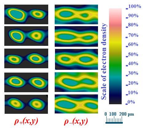
American Journal of Engineering Research (AJER)                                                            2012
Schrödinger equation can be given in a form Ψ(1,2) = С1Ψ1 + С2Ψ2 , where С1 and С2 are arbitrary coefficients
that satisfy the physical condition of the problem.
In fact, the square of the function characterizes the probability density of the simultaneous presence of the first
and second electrons at certain distances from the nuclei. Since it is impossible to distinguish electrons, the
condition must be true Ψ2(1,2) =Ψ2(2,1), that is, the square of the function Ψ(1,2) should not change its value
when the electrons are rearranged. Obviously, this is true only when С1 = С2, ie Ψ can have only two values:
Ψ+(1,2) = С(Ψ1 + Ψ2) and Ψ-(1,2) = С'(Ψ1 - Ψ2).
The function Ψ+(1,2) is symmetric, it retains its value when the electrons are rearranged. The function Ψ-(1,2) is
anti-symmetric; when the electrons are rearranged, it changes sign.
Therefore, instead of the initial functions Ψ1 and Ψ2, we obtained the functions Ψ+ and Ψ-, which determine the
covalent chemical bond that arises due to the hybridization of electron clouds.
Given the above, the total wave function of two atoms bonded by a covalent bond takes the following form:
Ψ (q) =φA(q)+φB(q)+Ψ±(q).

                            III.     ELECTRON CLOUD DENSITOMETRY
A direct image of an electron cloud can be obtained due to the electron beam shifting effect by passing a plane
wave of electrons through atoms. The quantum theory of the electron beam shifting effect was elaborated by the
O.P. Kucherov and others [4,5].
Using the theory of electron beam shifting effect, we find how a plane electron wave interacts with covalently
bound atoms.
As is known, the wave function of a beam of electron rays propagating along the z axis is a plane wave:
 Ψ(z) =√j exp(ikz),
where j is the electron beam density; k is a constant for a plane wave.
Based on the principle of superposition, the wave function of a system of two atoms plus the beam of electron
rays is the product of their functions:
Ψ (q, z) =√j exp(ikz){φA(q)+φB(q)+Ψ±(q)}.
The probability density is the square of the modulus of this function. Let's find him.
Ψ 2(q, z)= j exp(2+ikz){φA(q)+φB(q)+Ψ±(q)}2
= j exp(2+ikz){φ2A(q) +φ2B(q) +Ψ2±(q)
 +φA(q)φB(q) +φA(q)Ψ±(q) +φB(q)φA(q) +φB(q)Ψ±(q) + Ψ±(q)φA(q) +Ψ±(q)φB(q) }.
According to the Pauli principle, the functions φA(q), φB(q) and Ψ±(q) are at different energy levels, ie if at some
point in the space q one of these functions is nonzero, the other function will necessarily be equal to zero.
Therefore, the last expression takes the form:
Ψ 2(q, z)= j exp(2+ikz){φ2A(q)+φ2B(q)+Ψ2±(q) } .
Take the integral of this expression over the variable z from the lower surface of the sample z0 to the upper zmax,
and for electron cloud densitometry we finally get:
ρ (x, y) = j{ρA (x, y)+ ρB (x, y)+ ρ± (x, y)}.
That is, the intensity of the electron beam passing through the atom is directly proportional to the thickness (path
length) of the electron cloud of the atom at the point of transmission of the rays.

                    IV.      EXPERIMENTAL PHOTO OF COVALENT BONDS
The silicon layer was grown at 650 ° C for 45 s. The height of an island is 6 nm, the width of the base - 12 nm.
In part, the problem of high defect of silicon layers on sapphire, which occurs in the initial stages of growth, was
removed by using UTSi technology (Peregrine corp.) [6]. Obtaining a cross section was carried out using special
equipment (Gatan 601.07000 TEM Specimen Preparation Kit), developed by Gatan, USA.
Electron cloud density technology was used to directly visualize chemical bonds. Images of silicon atoms
together with their symmetrical and anti-symmetric covalent bonds were obtained.
Direct images of crystalline silicon atoms with chemical bonds were studied using a transmission electron
microscope JEM2100F (JEOL, Japan).
An experimental method [7] of electron cloud densitometry which based on the electron beam shifting effect
[4,5] with resolution of 10 picometers was used.

 www.ajer.org                                                                                             Page 55
 www.ajer.org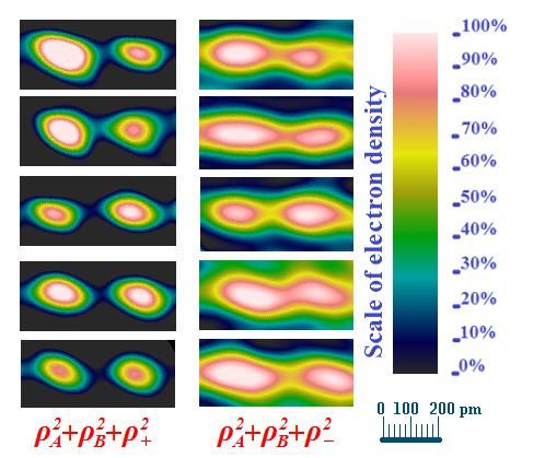
American Journal of Engineering Research (AJER) 2012
Figure 1: Photos of electron clouds of silicon atoms symmetric ρA(x,y)+ρB(x,y)+ρ+(x,y) and anti-symmetric
ρA(x,y)+ρB(x,y)+ρ-(x,y) covalent bonds. The electron clouds of the inner electrons ρA(x,y) and ρB(x,y) are pink.
Valence electrons are green - symmetric ρ+(x,y) on the left, anti-symmetric ρ-(x,y) - on the right.
Fig. 1 shows photos of five electron clouds of silicon atoms symmetric ρA(x,y)+ρB(x,y)+ρ+(x,y) and anti-
symmetric ρA(x,y)+ρB(x,y)+ρ-(x,y) covalent bonds. The electron clouds of the inner electrons ρA(x,y) and ρB(x,y)
are pink. Valence electrons are green - symmetric ρ+(x,y) on the left, anti-symmetric ρ-(x,y) - on the right. The
scale of electron cloud density and length scale are given next to it.
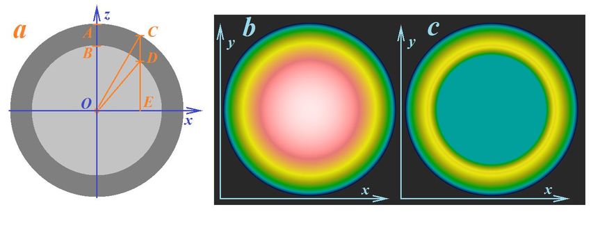
V. GEOMETRY OF ELECTRON CLOUDS
Fig. 1 shows the photos of the total contribution of bonding and remaining electrons. Schematically, these two
clouds are presented in Fig. 2a. The cloud of remaining electrons is a sphere of radius OB, and the bonding
electron is a shell with a thickness of BA. According to the electron beam shifting effect, in the center of the
atom with coordinates x = y = 0 (see Fig. 2a), all electrons make the same contribution to the total intensity
(100%).
Thus, the contribution of all 14 silicon electrons is characterized by a segment OA, which consists of one
bonding electron (segment BA) and remaining electrons (segment OB). Therefore, from the ratio 100% / x =
14/1 for the contribution of the bonding electron we find x = 7%.
The contribution of the binding electron at any distance from the center OE can be found from the following
relation.
The intensity of the electron density of the clouds will be equal to EC-ED, and EC is from the experiment, and
ED - from two right triangles: OCE and ODE. The following conditions allow to solve this problem: OD = OB
and OC = OA.
www.ajer.org Page 56
www.ajer.orgAmerican Journal of Engineering Research (AJER) 2012
Figure 2: Technology of separation of an individual electron cloud from an atom: a) geometry of the thickness
of electron clouds of bonding and remaining electrons, side view; b) model of the atom ρA(x,y)+ρB(x,y)+ρ+(x,y);
c) model of the separated bonding electron cloud ρ+(x,y), top view.
To illustrate this, a model of the silicon atom was made in accordance with the Fermi-Thomas model
(E. Fermi, L. Thomas, 1927), which works for atoms of any complexity. The method uses a quasi-classical
approximation: each atom of the periodic table has a certain radius r (Bohr radius), so at the distance a r the electron density is small and decreases
exponentially.
Fig. 2b shows the model of the atom with all electron clouds ρA(x,y)+ρB(x,y)+ρ+(x,y). Fig. 2c shows the
model of the electron cloud of the separated bonding electron cloud ρ+(x,y).Using the technology of electron
cloud geometry, from the photo of five electron clouds of silicon atoms, Fig. 1, the contribution of the remaining
electrons ρA(x,y)+ρB(x,y) was subtracted.
Figure 3: Electron cloud density distribution of non-hybridized ρ+(x,y) and hybridized ρ-(x,y) covalent bonds
obtained by subtracting the electron cloud density of remaining electrons ρA(x,y)+ρB(x,y) .
www.ajer.org Page 57
www.ajer.orgAmerican Journal of Engineering Research (AJER) 2012
Fig. 3 shows the electron clouds of pairs of silicon atoms not hybridized ρ+(x,y) and hybridized ρ-(x,y) by
covalent bond.
As a result, we see that during hybridization, the electron clouds of binding electrons do not overlap, but form a
single cocoon stretched in the middle.
VI. CONCLUSION
The advent of electron density densitometry makes every atom visible in molecules with a wide range
of chemical bonds. The method of electron density densitometry not only makes it possible to see the molecular
structure of already known molecular crystals, but also to discover new ones with extraordinary technological
properties. For example, a two-layer diamond gubanite [5] and superdense two-layer diamond-like carbon
allotrope, rudenite [4].
In this work, quantum-mechanical calculations of the covalent bond were developed for the general
case of any identical atoms of the periodic table. The solution of the Schrödinger equation due to the electron
beam shifting effect is found. A number of photos of silicon atoms in the state of symmetric and anti-symmetric
covalent bonds were obtained by densitometry of electron cloud density. The geometry of the electron cloud
developed in this paper separates the form of pure covalent bonds of silicon atoms from the general photo of
atoms.
REFERENCES
[1]. Omehe N. N., Otete I. "Ab initio study of the electronic band structure and phonon dispersion spectra of Silicon disulphide ( SiP2)
and Silicon diarsenide (SiAs2)." American Journal of Engineering Research (AJER), vol. 6, no. 12, 2017, pp. 439-447.
[2]. Bohr, Niels (1913). "On the Constitution of Atoms and Molecules, Part III Systems containing several nuclei". Philosophical
Magazine. 26 (155): 857–875. doi:10.1080/14786441308635031.
[3]. Heitler, W.; London, F. (1927). "Wechselwirkung neutraler Atome und homoopolare Bindung nach der Quantenmechanik"
[Interaction of neutral atoms and homeopolar bonds according to quantum mechanics]. Zeitschrift fur Physik. 44 (6–7): 455–472.
[4]. Kucherov, O. P.; Rud, A. D. (2018). Direct visualization of individual molecules in molecular crystals by electron cloud
densitometry. Molecular Crystals and Liquid Crystals 674 (1): 40–47. doi:10.1080/15421406.2019.1578510.
[5]. Kucherov O., Rud A., Gubanov V., Biliy M. Spatial 3d Direct Visualization of Atoms, Molecules and Chemical Bonds // American
Journal of Applied Chemistry. — 2020. — Т. 8, № 4. — С. 94—99. DOI: 10.11648/j.ajac.20200804.11
[6]. US Patent 5.973.363. Oct. 26, 1999. CMOS circuit with shorted p-channel length on ultrathin silicon on insulator.
[7]. Kucherov O.P., Lavrovsky S.E., Patent of Ukraine № 115602 From 27.02.2018, "Method of obtaining an image with subdiffraction
resolution and optoelectronic system for its implementation".
Kucherov O. P. "Direct Visualization of Covalent Chemical Bonds in Crystalline
Silicon.”American Journal of Engineering Research (AJER), vol. 10(6), 2021, pp. 54-58.
www.ajer.org Page 58
www.ajer.orgYou can also read