Gallium Nitride: Catalyst for the Next Generation of Power
←
→
Page content transcription
If your browser does not render page correctly, please read the page content below
Gallium Nitride: Catalyst for the Next Generation of Power
 Gallium Nitride (GaN) comes-of-age to meet 5G needs, enable new topologies
                        and revolutionize fast charging.
                              by Stephen Oliver

Smartphone screens, batteries and increased 5G features with intensified data processing
and transmission rates and volumes have put a spotlight on charging speeds and the size,
weight and cost of leading-edge travel adapters. At the same time, the introduction of a
single, flexible charging platform (hardware and software) – i.e. the universal serial bus
‘Type-C’ connector (USB-C) with power delivery (USB-PD), or programmable power supply
(PPS) - means that consumers are no longer tied to one OEM’s power offering. Now, a user
can choose one charger that has enough power for their big MacBook Pro 16”, and the
same device can power their phone or earbuds safely and quickly.
Since 2010, the average screen size (cm 2) and battery capacity (mAhrs) for new phone
platforms like the Apple iPhone 12, Xiaomi Mi11 and Samsung S21 have increased over 3x,
as shown in figure 1 (compiled from data published by GSMArena). Using slow, silicon-
based 5W or 20W commodity ‘in-box’ chargers leads to unacceptable, extended charging
times, so more power is required. To get more power from a silicon charger means more
size, more weight and more cost – as traditional, low-frequency topologies dictate that
designs are power-density and heat-density limited.

Figure 1: Smartphone screen-size and battery capacity h as increase d over 3x in 10
years. As new platforms have been rel eased with faster charging rates, OEMs have
moved to adopt gallium nitride (GaN ) chargers for both accessory and ‘in -box’ options.
Source: GSMArena, Navitas as of January 2021.

The key to improved power density is increased switching frequency to minimize passive
components such as transformers, EMI filters, bulk and output capacitors, etc. High-speed
topologies such as the active-clamp flyback (ACF) have been proposed by academics since
1996i but were frustrated by silicon’s poor on-state (RDS(ON)) and switching (QGD, Trr, COSS)
performance plus complexity and lack of optimized control ICs. In early 2018, the
introduction of the GaN power IC ended that frustration and enabled commercial viability of
not only the ACF but also high-frequency quasi-resonant flyback for smartphone chargers,
plus topologies such as CrCM boost PFC, high-speed LLC and advanced CrCM totem-pole
                                                                                                1.
                                                                                            1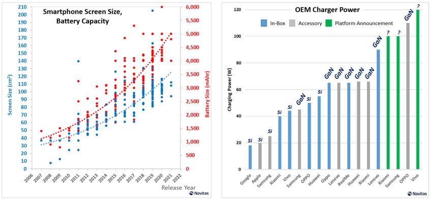
PFC for higher-power systems such as gaming laptops, all-in-one PCs, TVs and 5G
transmitter cell power.
A gallium nitride power IC monolithically-integrates GaN power (FET) and GaN drive plus
control and protection in a single SMT package. These “GaNFast™” power ICs become
easy-to-use, high-speed, high-performance ‘digital-in, power-out’ building blocks. Integration
enables virtually zero loss in turn-off because the gate drive loop has essentially zero
impedance. In addition, turn-on performance can be controlled and customized for specific
application requirements.
The result is that GaN power ICs enable 3x faster charging in half the size and weight vs.
old, slow, silicon-based designs, and have been adopted by tier-1 OEMs such as Dellii,
Lenovoiii, and Xiaomiiv for smartphone and laptop fast charging.
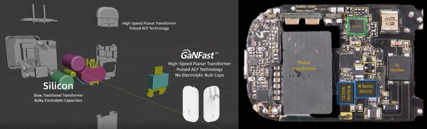
A closer look at the OPPO 50W Mini SuperVOOC “Cookie” fast charger highlights how a
high-speed, GaN-enabled topology minimizes or eliminates passive components.
The OPPO 50W Mini uses a 10x higher-speed, high-efficiency ‘active-clamp’ flyback using
TI’s UCC28782 controller with a pair of GaNFast power ICs in a half-bridge configuration.
High-speed operation (~400 kHz) is possible due to the ‘soft-switching’ topology and the
GaNFast power ICs with extremely low resistance (R DS(ON) to minimize ‘on-state’ losses, and
minimal output capacitance (C OSS) for the best ‘switching’ performance. High-speed now
means that the main isolating transformer, EMI filter, output smoothing capacitors, etc. can
shrink in size and cost.
Figure 2: OPPO 50W Mini “Cookie” charger, showing high -frequency planar
magnetics and elimination of electrolytic bulk capacitor.
In a traditional charger, a large part of the total size is due to the electrolytic ‘bulk capacitor’
used to smooth out ripple from the rectified AC input prior to the down-converting flyback.
The ‘bulk cap’ can occupy 40% of the total charger size. In the 50W Mini design, a
proprietary innovation creates the world’s first charger using ‘pulsed’ power conversion. This
eliminates the electrolytic bulk capacitor, and the rectified 100 Hz pulsating DC feeds directly
into the high-frequency ACF circuit which can maintain a smooth output to charge the
phone’s battery, even when the input voltage range is wide. This OPPO-proprietary ‘direct-
charge’ approach means that during each pulse gap, the polarization effect in the phone
battery is eliminated so reducing wear-out mechanisms and extending battery life.
Traditional transformers operate at a few 10’s of kHz and are constructed using toroidal
ferrite cores, with separate wire-windings (primary and secondary) to isolate and convert
voltage. As operating frequencies increase, a new flat or ‘planar’ transformerv can be created
in which the primary and secondary windings are embedded into PCB material – resulting in
2.
2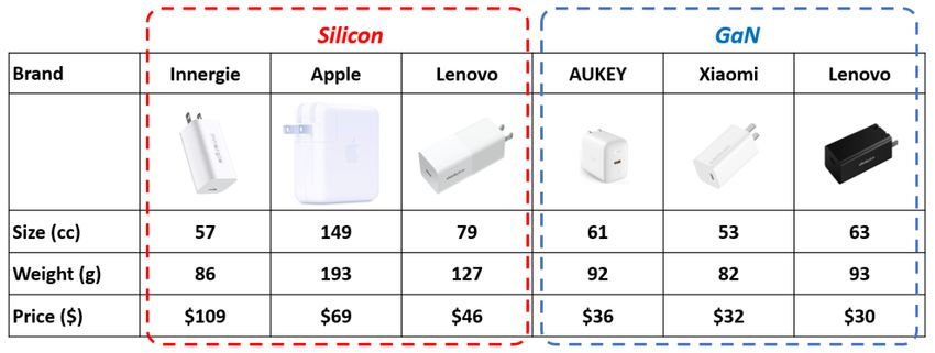
extremely efficient, high-frequency, low-profile and low-noise (low EMI) systems, while
utilizing more automated manufacturing methods for more consistent performance.
Overall, the size difference can be seen comparing a traditional topology with wire-wound
transformer (typically over 20 mm) plus large electrolytic bulk capacitor, against the OPPO
50W Mini with new 400 kHz, 8 mm planar transformer and no electrolytic capacitor. The
high-speed GaNFast-based Mini is less than half the size of the old, slow, silicon-based
version.
Unlike most new technologies that are burdened with a significant price-tag that limits
adoption, the system benefits – and system cost – of GaN-enabled, high-speed chargers
mean that retail price is lower than the previous best-in-class silicon designs, as shown in
figure 3.

Figure 3: GaN -enabled chargers average half the size, weight and price of previous
best-in-cl ass silicon chargers (61W -65W, retail pricing at launch).

To take this one step further, in December 2020, Xiaomi launched the Mi 11vi without a
charger in the box, and offered users a simple choice: use an existing charger (and avoid
CO2 emissions related to manufacturing and shipping), or receive a GaNFast 65W charger…
for free.
As of January 2021, 13M GaNFast power ICs had been shipped with zero failures.vii 40
years after the silicon bipolar junction transistor gave way to the switching silicon MOSFET,
we are seeing the ‘second revolution’viii in power electronics, with gallium nitride as the
enabling catalyst.

                                                                                                    3.
                                                                                                3
i
   R. Watson, F. C. Lee and G. C. Hua, "Utilization of an active-clamp circuit to achieve soft switching in
flyback converters," in IEEE Transactions on Power Electronics, vol. 11, no. 1, pp. 162-169, Jan.
1996, doi: 10.1109/63.484429.
ii
    “Dell Adopts Navitas GaNFast Technology for Laptop Fast Charger”, December 2020,
https://www.navitassemi.com/dell-adopts-navitas-ganfast-technology-for-laptop-fast-charger/
iii
    Lenovo Legion phone launched with 90W GaNFast charger, July 2020
https://www.navitassemi.com/lenovo-partners-with-navitas-again-to-deliver-the-worlds-first-ganfast-
90w-fast-charger-for-e-sports-mobile-phones/
iv
     “Navitas‘65W GaNFast charger solution chosen by Xiaomi for Mi 10 Pro”, Navitas, February 2020,
https://www.navitassemi.com/navitas65w-ganfast-charger-solution-chosen-by-xiaomi-for-mi-10-pro/
v
    Xiucheng Huang, Navitas, “GaN ICs Enabling Next-Gen ACF for Adapter/Charger Application” at
APEC 2019, https://www.navitassemi.com/download/gan-power-ics-enabling-next-gen-acf-for-
adapter-charger-applications/?wpdmdl=36529&ind=1561100214576
vi
     “Xiaomi Mi 11 arrives as the first phone with Snapdragon 888”, GSMArena, December 2020,
https://www.gsmarena.com/xiaomi_mi_11_arrives_as_the_first_phone_with_snapdragon_888_brings
_1440p_screen-news-46923.php
vii
     “Navitas Ships 13,000,000 GaNFast Power ICs with World-Class Reliability”, Navitas, January
2021, https://www.navitassemi.com/navitas-ships-13000000-ganfast-power-ics-with-world-class-
reliability/
viii
  “From Science Fiction to Industry Fact: GaN Power ICs Enable the New Revolution in Power
Electronics”, Oliver, Xue & Huang, Bodo’s Power December 2017
https://www.navitassemi.com/download/from-science-fiction-to-industry-fact-gan-power-ics-
enable-the-new-revolution-in-power-electronics/?wpdmdl=37063&ind=1562849999810
.

.

.

.

.

.

..

                                                                                                              4.
                                                                                                         4
You can also read