H2020 CABRISS Public Business Plan - Zenodo
←
→
Page content transcription
If your browser does not render page correctly, please read the page content below
H2020 CABRISS Public Business Plan
CABRISS – Grant Agreement 641972 – Public Business Plan

The CABRISS Public Business Plan is a deliverable of the CABRISS project.

  Project coordinator and contact:          David Pelletier and Jean-Patrice Rakotoniaina
                                            Commissariat à l’énergie atomique et aux énergies
                                            alternatives (CEA)
                                            50 avenue du Lac Léman | F-73375 Le Bourget-du-Lac
                                            Email: david.pelletier@cea.fr
                                                    jeanpatrice.rakotoniaina@cea.fr

  Authors:                                  Marie-Charlotte Hoffmann and Harald Suitner
                                            PROJEKTkompetenz.eu GmbH, Franz Josef Straße 19, A-5020
                                            Salzburg │
                                            Robert Thomas
                                            Commissariat à l'Energie Atomique
                                            et aux Energies Alternatives (CEA)
                                            MINATEC Campus | 17 rue des Martyrs | 38054 Grenoble
                                            Cedex 9
                                            Inputs from all consortium partners

  Website:                                   www.spire2030.eu/cabriss

                                                   DISCLAIMER
The information in this document reflects only the author's views and the European Commission is not liable for
any use that may be made of the information contained therein. The information in this document is provided
"as is" without guarantee or warranty of any kind, express or implied, including but not limited to the fitness of
the information for a particular purpose. The user thereof uses the information at his/ her sole risk and liability.

                     The CABRISS project has received funding from the European Union’s Horizon
                     2020 research and innovation programme under grant agreement No 641972.

                                                                                                  Page 2 of 26
CABRISS – Grant Agreement 641972 – Public Business Plan

1. Challenge and opportunity of Photovoltaic waste ................................................................. 4
2. CABRISS in brief ........................................................................................................................ 8
3. CABRISS Recycling .................................................................................................................. 11
   3.1 Primary recycling and recovery of secondary materials from complex PV waste ................... 11
   3.2 Recycling of silicon powders from kerf ...................................................................................... 12
   3.3 Purification of recycled silicon from end-of-life PV wastes and kerf to solar grade ............... 13
4. CABRISS Intermediate Products: reuse of recovered materials .......................................... 14
   4.1 Conductive inks and pastes produced from recovered silver .................................................. 14
   4.2 Indium sputtering targets produced from recycled indium ..................................................... 15
   4.3 Production of wafers from recovered silicon ............................................................................ 16
5. CABRISS Sustainable PV Production ...................................................................................... 18
   5.1 Standard production of PV cells and modules from recycled materials .................................. 18
   5.2 CABRISS Life Cycle Analysis ......................................................................................................... 19
6. Economic perspectives........................................................................................................... 20
7. Conclusions ............................................................................................................................. 23
8. Glossary ................................................................................................................................... 24
9. References .............................................................................................................................. 25
10.       List of Figures and Tables ................................................................................................ 26

                                                                                                                            Page 3 of 26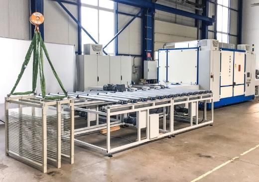
CABRISS – Grant Agreement 641972 – Public Business Plan

Photovoltaic waste – types and expected volumes
20 years ago the photovoltaic (PV) industry started to grow predominantly in Europe and the United
States. Today, production has reached a capacity of close to 60 gigawatts (GW), of which only 5% are
produced in Europe. With an average solar panel lifetime of 25-30 years, the first wave of end-of-life
PV wastes is expected in Europe, while production wastes are today predominantly generated in
China and the rest of Asia. During PV production, some wastes are fully recycled within the process
(high-quality silicon which is cut off when shaping ingots into bricks). Other wastes cannot be reused
directly in a closed loop: the abrasive slurries generated during sawing (ingot to brick, and cutting
wafers from the brick) contain large quantities of silicon (Si) powders – Si kerf. In this way, 55% of the
input silicon feedstock are lost as kerf during production. Another source of wastes occurs through
breakage during production (solar cells), or transport and handling of the modules and leads to
complex wastes that have to be recycled in the same way as end-of-life modules.
Solar panels differ widely in terms of architecture, technology and composition of materials. This has
to be considered in the development of recycling business models. PV technologies based on silicon
wafers account for 93% of the production in 2015. In the same year, the market share of thin film
technologies amounted to 7% worldwide1.
In 2016, losses arising from initial transport/installation damage or from very early installed system
failure are still greater than “true” end-of-life wastes. In a near-term scenario for end-of-life panels
included in the CABRISS market analysis, it is estimated that only from 2020 on, waste streams from
end of life panels will be comparable with, or greater than transport and installation wastes.

1
    CABRISS Market and Competitive Analysis (internal document)

                                                                                          Page 4 of 26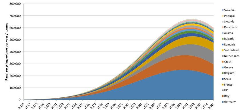
CABRISS – Grant Agreement 641972 – Public Business Plan

     Figure 1: Yearly waste volumes (panel lifetime 30 years, slope factor 5.376. Source: CABRISS Market Analysis)

As can be seen from Figure 1, end-of-life waste volumes and values are expected to rise steeply after
2020, peaking in 2041-2042. The European countries that have been the earliest adopters of solar
technologies, will experience the first large wave of wastes, among them Italy, the UK, France, and
with the highest share, Germany.
PV modules – architecture and composition
In principle, PV modules consist of a high-quality and therefore expensive, iron-free glass panel which
covers the front side and an absorber layer which is encapsulated with Ethylene Vinyl Acetate (EVA).
On the back side, the panel is protected either
by a composite-layer backsheet foil (Si PV
modules) or by another glass panel of lower
quality (thin film PV modules). This sandwich is
a tightly bound and complex material mix,
which is not easy to recycle. The low-hanging
fruit from the recycling point of view are the
aluminium frame, the copper cables and the
inverter box which have to be delivered
complete to the primary recycling facility (e.g.
by regulation in Germany).                                      Figure 2: Si PV module architecture

The proportion of glass in Si PV panels is
typically 70-76%, and can reach even 90-98% in glass-glass thin film panels. However, the proportion
of materials in the panel composition varies not only according to panel technology but also as a
function of the year of production. In Si-based solar cells, the charge carriers generated in the silicon
absorber layer are transported by a conductive printed structure made from silver pastes. In the last
5 years, Si PV manufacturers have achieved a significant (threefold) reduction of silver usage.

                                                                                                      Page 5 of 26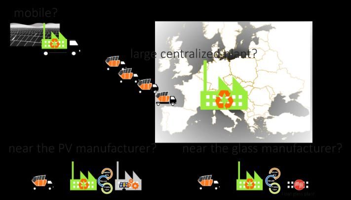
CABRISS – Grant Agreement 641972 – Public Business Plan

Between 1990 and 2010, the silicon content of PV panels has decreased by nearly one third2. That
means that the first wave of end-of-life Si PV wastes contains the highest amount of the most valuable
materials, silicon and silver. Recyclers are under pressure to establish technologies that allow a cost-
efficient recovery of these materials.
The mass balance of a typical Si PV panel (to the right)
illustrates that mere recycling of glass, aluminium and
copper cables achieves a recovery rate of more than 90%
of the waste. For thin film PV, the proportion is even
higher. Aluminium frame and copper cables with
junction boxes can be easily separated from the panel
sandwich, which can then be crushed in order to remove
the organic materials. The residues can be quite easily
recovered in refineries that purchase electronic scrap.
But it is difficult to separate the silicon effectively

                                                                                                     Junction
without driving up the cost for the recycling process.                                   Backsheet

                                                                                                       box
                                                                                  EVA
The most common thin film technologies are CIGS                                                     Cop-
                                                                                          Silicon
(copper-indium-gallium-diselenid) and CdTe (cadmium                                                 per
                                                                                                  Silver
tellurite). A CIGS module is produced by deposition of a
thin-film of a CIGS alloy typically on glass, using ITO Figure 3: Mass balance Si PV panel waste
(Indium Tin Oxide) or indium sputtering targets. Within the active absorbing layer, indium is by far
the most expensive component, though gallium is also valuable. Producers therefore seek to reduce
the production cost by reduction of layer thicknesses of the CIGS active layer – which is limited the
light absorption efficiency would be reduced if the layer got too thin.
WEEE and collection of PV waste - precondition for an emerging business opportunity
In 2007, the PV Cycle Association (European Association for Volontary Take Back and Recycling of PV
Modules) was founded as NGO in order to prepare the European PV sector for the steep increase of
PV end-of-life waste streams. PV Cycle has paved the way for the first legal framework on PV waste
worldwide which is included in the revised WEEE directive of 20123 and based on the extended-
producer-responsibility principle (EPR). In short, the extended-producer-responsibility ensures that
all EU market participants - independent of their location - are liable for the cost of collection,
treatment and monitoring of PV waste and must fulfil financing, reporting and information
responsibilities. The directive sets the targets to collect 85% of waste generated, to recover 85%, and
to recycle and prepare for reuse 80% (figures given will be valid from August 2018, current targets
are slightly lower). The WEEE requires a „high-value recycling approach“ addressing not only
potentially harmful substances, but also rare materials like silver and indium, or materials with highly
embedded values (silicon and glass).4 However, specific target recovery rates for such materials are
not included.

2
    CABRISS Market and Competitive Analysis (internal document)
3
    Directive 2012/19/EU of the European Parliament, July 2012
4
    IRENA_IEAPVPS_End-of-Life_Solar_PV_Panels_2016 Report

                                                                                        Page 6 of 26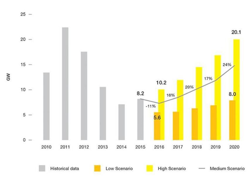
CABRISS – Grant Agreement 641972 – Public Business Plan

The implementation of the WEEE into national law, has been ongoing in some member countries
until 2016. Therefore, no EU-wide statistical data about collection rates are currently available. But it
is clearly visible that national regulations have broadened and strengthened the business case for a
variety of actors for PV waste recycling in Europe. Among member states, the WEEE directive is
implemented with individual variations. E.g. in Germany, the implementation of the
“Elektroaltgerätegesetz” (Electrical and Electronic Equipment Act) is coordinated by a national
clearing house (Stiftung EAR/Elektro-Altgeräte Register), while a number of service providers (e.g. PV
Cycle Germany, take-e-way, European Recycling Platform/Land bell) for PV compliance, take-back
and recycling share the actual collection of PV waste and organise recycling with certified primary
recycling facilities (to whom they deliver wastes for a service fee). In France, PV take back and
recycling is organised centrally. PV CYCLE France is approved by the public authorities for the
management of PV wastes and collects and recycles the entire available waste. Panels are effectively
processed with a contract partner (Veolia) at a central treatment site which will enable the recycling
of more than 1,400 annual tonnes of materials by the end of 2017.
Recycling of PV wastes: state of the art
Before the implementation of the WEEE directive in Europe, several attempts were made to identify
economically viable solutions for PV recycling. In 2009, a process based on thermal treatment of
modules followed by chemical treatment was implemented at an industrial scale by the SolarWorld
subsidiary Sunicon 5. Sunicon started operations in 2004, but in 2013 the recycling facilities stopped
operations after the spot market prices for solar grade silicon had collapsed6. In the United States,
where up to now no regulation for recycling of PV wastes exists, analyses on the profitability of
recycling protocols for different PV end-of-life wastes have calculated an economic viability only for
recycling of CIGS systems 7. It was clearly stated that recycling of Si PV systems results in higher cost
than profit. The study concluded that recycling of PV systems should be supported by government
policies. In 2013, it became obvious that module producers are not the main players in the PV
recycling market. Other recyclers reach a sufficient recovery rate by processing just aluminium,
copper and low-quality glass. The WEEE targets from 2018 on – requesting recovery of 85% of the
mass – address only 21% of the potential value of silicon solar panels (glass being 70-76% of the
weight, and aluminium 10-13%, according to the CABRISS market analysis). That means that valuable
materials do not necessarily have to be recycled to reach the set target rate. Since then, many
technological approaches for recycling of Si PV at industrial scale have received national and EU
funding, but no technology has been able to recover all reusable materials based on an economically
efficient business model.
To be ready for the expected PV waste streams, CABRISS supports the development of innovative
technologies by close collaboration between recyclers and users of the recovered materials.

5
    Wambach et al., 2009
6
    Rentzing, 2010
7
    Mcdonald and Pearce, 2010

                                                                                         Page 7 of 26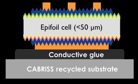
CABRISS – Grant Agreement 641972 – Public Business Plan

CABRISS8 is a EU funded 3 year project (Horizon2020 Innovation Action, 06/2015 to 06/2018) and
targets a circular economy for photovoltaic products. The focus is on the development of
technologies for eco-efficient recovery of secondary materials from PV end-of-life modules and PV
production wastes, enabling the reuse for a cradle-to-cradle production of PV modules.
In short, CABRISS offers solutions on three levels:
                                      CABRISS ensures economically viable high-value recovery of
                                      secondary materials from:
                                       ✓ complex PV wastes (end-of-life & broken modules /cells)
                                       ✓ silicon kerf (diamond wire & block cutting)

                                      CABRISS develops innovative approaches for cost-efficient reuse
                                      of the recovered materials in high-quality products (silicon
                                      powders; conductive inks and pastes; sputtering and ITO targets;
                                      wafers and low-cost wafer equivalents).

                                      CABRISS enables a sustainable, resource- and cost-efficient
                                      manufacturing of PV cells & modules from recovered materials.
The actors in CABRISS cover the full value chain starting from waste collection and resulting in a closed
loop reuse of secondary materials for PV production. The CABRISS business approach is based on
innovative recycling of indium, silver, silicon and high-quality glass which can obviously also be used
in other markets than PV. But closing the loop is an important feature of the project: it allows to
assess the cumulated carbon footprint reduction for PV modules achieved by using recycled
materials. In addition, several innovative, resource-saving production technologies are developed for
wafers and solar cells.

►      5 Research institutes
►      11 Companies
►      9 EU countries
►      2 Value chains

8
    www.spire2030.eu/cabriss

                                                                                         Page 8 of 26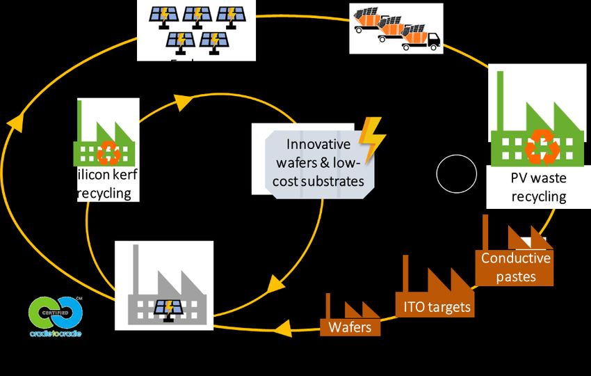
CABRISS – Grant Agreement 641972 – Public Business Plan

Partners and their role in the project value chain:

                  Collection of PV modules

                  Recycling of PV modules, recovery of silicon, indium, silver and high-quality glass
                  from PV waste

                  Recycling of silicon kerf

                  Purification of silicon (powders and demetallized silicon shards)

                  Conductive pastes and inks from recovered silver

                                                                                                        COMPANIES
                  Hot pressing ingots
                  ITO and sputtering targets
                  Silver flakes and silver coated copper particles

                  Thermal spray of silicon for free standing wafers and wafer equivalents

                  Ingot growth from secondary silicon

                  Manufacturing of Si PV cells and modules

                  Manufacturing of thin film PV modules

                  Coordination support, business models

                  Wafering and etching

                  Manufacturing of low-cost wafers and substrates from Si kerf
                                                                                                        RESEARCH

                  Production of HET cells on low-cost substrates

                  Materials and devices modelling, characterization, dissemination, exploitation,
                  standardization, Life Cycle Analysis
                  Coordination
                  Secondary silicon purification and reuse in PV chain (ingot growth, manufacturing
                  of cells and modules)

                                                                                              Page 9 of 26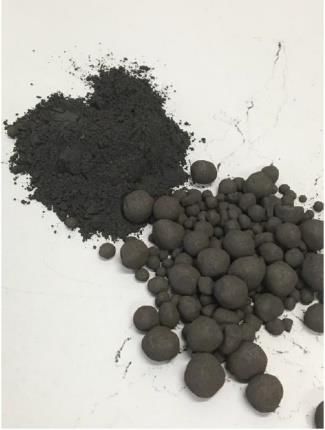
CABRISS – Grant Agreement 641972 – Public Business Plan

                                                          Arrows depict partners‘ activities
                                                                   LOSER
                                                                   FAID/FERROPEM/SFS
                                                                   RESITEC
                                                                   RHP
                                                                   PYROGENESIS
                                                                   SOLITEK
                                                                   INKRON
                                                                   SUNPLUGGED
                                                                   ECM
                                                                   Research (THM/CEA/
                                                                   SINTEF/IMEC)
                                                                   external contractors

                                                                Recovered from kerf
                                                                Recovered from PV
                                                                cells & modules
                                                                CABRISS products
                                                                (conventional route)
                                                                CABRISS products
                                                                (innovative route)
                                                                PV manufacturing

Figure 4: Overview of the CABRISS value chain

                                                                        Page 10 of 26
CABRISS – Grant Agreement 641972 – Public Business Plan
3.1 Primary recycling and recovery of secondary materials from complex PV waste
Where is the problem?
Today, technologies for high-value recycling of PV wastes (targeting a recovery of all reusable
materials) are not cost-efficient. PV panels are a complex waste with a rather low density of valuable
materials, recycling cost depend on the PV technology (thin film, Si PV) and module architecture,
resale values on content and (fluctuating) resale prices of materials. Many recyclers focus therefore
on keeping cost low, treatment of end-of-life and broken modules is mostly done by removing the
aluminium frame, junction box and copper cables, and shredding the glass with attached organic
encapsulants/silicon cells and absorber layers. The organic material is then usually removed by
thermal treatment of the total mass, the glass mostly reused in low quality applications (glass wool),
and silicon is not recovered.
What is the solution?
New technology and equipment for automatized opening and delamination of PV end-of-life
modules: the first economic solution in the market which does not shredder PV waste but is able to
recover undamaged glass – if modules are delivered without damage. Higher cost for damaged PV
wastes are compensated with a higher recycling fee at delivery. RESITEC and FAID are already
approved separation and sorting of several plastics and inorganic materials (for c-Si-Types) and
hydrometallurgical treatment to recover metals. Undamaged glass panels can be sorted according to
quality, separating the expensive, iron-free front glass panels from the rest.
Outputs are:
• Glass (sorted panels and sorted cullets)
• Aluminium, copper and/or stainless steel scrap
• De-metallized silicon shards (not purified)
• Silver (and/or compounds)
• Indium concentrates
• PAC (Poly Aluminium Chloride) recovered from
back-contact aluminium
Figure 5: LOSER glass recovery pilot line
What is new?
✓ High-Value recycling
Recovering all rare materials (silver, indium, gallium, tellurium, molybdenum)
Preserving quality and high-embedded energy values of silicon and glass
Securing potential harmful substances as lead, selenium, or cadmium
✓ “Zero waste” recycling
Reuse of low-value materials (EVA) is under evaluation
✓ High-yield recycling
Processing all types of PV waste (thin film and silicon PV)
Page 11 of 26CABRISS – Grant Agreement 641972 – Public Business Plan
Targeted recovery rate: 100%
Customers and markets
In Europe, the implementation of the WEEE supports the development of PV waste recycling as a
service. High-value recycling targeting the recovery of a maximum of reusable materials is a complex
and costly process. For end-of-life PV panels that are delivered undamaged to the recycling site, the
novel delamination technology leads to increased resale values from the material with the highest
mass in PV waste: glass. A mixed calculation based on these revenues and supported by the recycling
service fee, enables the economically efficient recovery of silicon, indium and silver. Customers are:
Specialised scrap processing facilities (aluminium, copper), glass manufacturing and recycling
industry, refineries, wastewater treatment plants and paper industry (PAC), PV manufacturers and
suppliers (de-metallized silicon, indium/compounds, silver/compounds). Options for the reuse of
glass panels (e.g. after surface treatment) will be further assessed in CABRISS.
3.2 Recycling of silicon powders from kerf
Where is the problem?
More than 50 percent of the input polysilicon feedstock are lost during PV production. Deposition of
these wastes in landfill has a negative environmental impact and means that the high energy invested
in the production of virgin silicon is lost. Up to now, cost efficient and safe recycling methods for Si-
kerf do not exist.
What is the solution?
Novel technology to recycle and manufacture low-cost silicon metal
powders from waste and deposited materials, leading to metallurgical
grade silicon. The novel technology developed by RESITEC for recycling
of silicon kerf from diamond wire cutting processes is cost efficient and
results in silicon powders with 1-5μm as D-50, 2-4 N (which means
99,00% to 99,99%) purity, low oxidation levels of 1-4% and low boron
and phosphorus content. Silicon kerf can be recycled into fine powders
or agglomerated to reduce dusting and dust explosion hazards, the
agglomerated material is suitable for melting in furnaces. Figure 6: Fine & agglomerated silicon
powders (photo RESITEC)
What is new?
✓ First technology for silicon kerf recycling with an industrial high yield process.
✓ Providing silicon powders with a significantly reduced carbon footprint.
✓ Recycling process without melting steps, built on unit operations with separation of particles,
chemical treatment, filtration of fine particles, drying and classification of particles.
✓ Unit operations can be combined and closely adapted to different industrial cutting process.
✓ Passivation of the surface of the silicon particles to avoid oxidation directly on site.
Page 12 of 26CABRISS – Grant Agreement 641972 – Public Business Plan
Customers and markets
PV manufacturing industry
PV manufacturers can reduce waste and save deposit cost, without investments or process line
modifications to implement Si-kerf recycling. Recycling of kerf will improve the environmental profile
of PV manufacturing and reduce the carbon footprint.
As the recycled powders have a metallurgical grade purity of 3-4N, there are today no commercially
known applications for recycled silicon metal powder in the PV manufacturing industry. However,
possible use in new low-cost solar cell concepts is tested in CABRISS.
Alternative markets for Si powders from kerf outside the PV industry
The main markets for metallurgical grade (2-3N) silicon powders from kerf are refractories, advanced
ceramics, silicon nitrides, silicones, additives to alloys, explosives, and batteries (R&D, TRL still low),
with a volume of several thousand tonnes per year in Europe. For some applications, the availability
of lower-cost Si powders recovered from kerf could boost the development (batteries, and other
high-tech applications).
3.3 Purification of recycled silicon from end-of-life PV wastes and kerf to solar grade
Where is the problem?
Silicon recovered from primary recycling of kerf has a rather low quality, and even silicon that has
been recovered from modules/broken cells cannot be used for the production of silicon wafers
without prior purification to solar grade (6N, i.e.99,9999% purity). Currently, the cost for purification
of silicon powders (from kerf) or shards (from modules recycling) to solar grade are high.
What is the solution?
Silicon recovered from different sources (kerf, demetallized broken cells, wafers or demetallized
silicon from end of life panels) is purified to a quality sufficient for PV applications or other specialty
applications (2-6 N purity). The purification process is characterised by a low energy consumption
and has a low carbon footprint. Demetallized broken cells, wafers and silicon from end of life panels
are treated by acid leaching, while silicon powders from kerf are purified by thermal treatment.
What is new?
✓ The resulting secondary silicon has a lower carbon footprint than virgin material.
Customers and markets
Customers for solar grade silicon are PV manufacturers (ingot and wafer production). For lower grade
purities, markets for advanced ceramics and metals (alloys) are addressed (see above).
Page 13 of 26CABRISS – Grant Agreement 641972 – Public Business Plan
4.1 Conductive inks and pastes produced from recovered silver
Where is the problem?
Silver is an expensive material which cannot easily be replaced, as its high conductivity is equalled or
overtaken only by even more expensive materials such as gold and platinum. The silver market
fluctuates according to demand, and the price volatility of silver is notorious. Virgin silver production
has well known damaging environmental effects (mercury
pollution). As already mentioned, the PV sector has put
efforts into reducing the silver consumption per solar cell,
but now seems to have reached a bottom line. Due to the
rising scale of global production, PV is responsible for 15%
of the overall market demand for silver. Silver is already
recycled in many industries (see Figure 69). The eco-
efficiency of PV should be increased by a further reduction
of silver consumption, recycling silver from PV waste and
using secondary material. Figure 7: Recycling of silver by sector. Source:
Metal focus, Silver Institute
What is the solution?
The use of secondary silver recycled from PV waste for the production of conductive pastes and inks
for PV manufacturing. The used polymer matrix is based on polysiloxanes which have superior
properties as opposed to acrylates, especially in terms of resistance to higher temperatures. In
addition, silver-coated copper particles have been tested as a lower-cost alternative. The results have
shown that the compatibility of the silver-copper particles with silver nanoparticles, added to
maximize conductivity, is excellent.
What is new?
✓ Using recycled silver will reduce cost and the demand for virgin silver in PV
production.
✓ Regenerating silver is a smaller burden for the environment
✓ Coating of copper particles reduces the overall silver consumption in PV
manufacturing. Figure 8: Silver paste
(symbolic)
Customers and markets
Customers for conductive pastes and inks made from recycled silver are the photovoltaic industry,
the (micro-)electronics sector, aviation and the automotive industry, printed electronics, producers
of displays, sensors, filters, and OLED’s (organic light emitting diodes), etc. IdtechEx estimates that
conductive inks and pastes market will reach nearly $1.7 billion in 2026 at current metal prices 10.
9
The_Silver_Institute, 2015
10
K. Ghaffarzadeh, 2017
Page 14 of 26CABRISS – Grant Agreement 641972 – Public Business Plan
4.2 Indium sputtering targets produced from recycled indium
Where is the problem?
Indium is a material that is widely used today, such as in TV- and PC-displays, PV, and other fields.
The market fluctuates, and prices remain rather high. The global demand is expected to grow steadily
with a share of indium consumption in the EU of around 10% of the world consumption. In the solar
sector, indium is mainly used for CIGS thin film solar photovoltaic technologies11. Today, indium is
mostly recycled only within the production process, from wastes that arise due to the inefficiency of
the ITO and indium sputtering process. The end-of-life recovery rate for indium is currently thought
to be very low due to the high cost of recycling.
What is the solution?
Indium sputtering targets and ITO targets were produced using secondary
indium recycled from thin film PV waste.
These targets have been successfully tested in thin film PV manufacturing. As
the recycling technology developed within CABRISS is expected to be cost
efficient on industrial level, the cost for recycled indium could be lower than Figure 9: Indium target
virgin material. (photo RHP)
What is new?
✓ First manufacturing of targets based on secondary indium recycled from PV wastes.
Customers and markets
Indium targets are used for manufacturing CIGS
(together with copper, gallium and selenium) and CIS
thin film solar cells. Indium-tin oxide (ITO) is deposited
by evaporation, vapor deposition or by using a
sputtering target as a thin film and acts as a transparent
electrical conductor. The largest application field is flat
screens, either liquid crystal displays (LCDs), plasma
display panels or screens employing OLEDs (organic light
emitting diodes).
The market is very large, stimulated by the boom of new Figure 10: Forecast net demand for Indium 2013,
and fast-growing digital-screen devices. For this market Source: Indium Corporation
sector, using recycled indium could be interesting to
increase the sustainability of the products, as first approaches towards closed-loop recycling (e.g. as
published by Dell in 2014) show. ITO was the largest application segment in 2015 and is expected to
exceed a total revenue of USD 400 million by 2025 12.
11
SETIS Materials Information System - Indium, 2017
12
Indium Market by Product, ba Application, by Region and by Segment Forecasts, 2016
Page 15 of 26CABRISS – Grant Agreement 641972 – Public Business Plan
4.3 Production of wafers from recovered silicon
Where is the problem?
The production of PV wafers is a very energy-intensive and costly process. At present, the cost of the
silicon wafer is responsible for roughly 40% of the PV module cost and for 20-30% of the carbon
footprint (depending on the Si-technology).
A set of solutions developed in CABRISS aims at tackling the following problems:
✓ High material cost of virgin silicon
✓ Silicon losses during brick cutting and wafering
✓ Costly, highly energy- and time-consuming production process
✓ Carbon footprint reduction
✓ Reuse of recycled silicon in high-value PV production chains
What are the solutions?
In CABRISS, the use of recycled silicon from different sources of PV waste (end-of-life, broken cells
and wafers, Si kerf) is tested in several conventional production processes. In addition, two highly
innovative technologies for a cost-, resource-, and energy-efficient fast production of PV wafers are
evaluated.
In a conventional industrial wafer production process, recycled silicon was introduced successfully.
Several silicon ingots were grown using 100% recycled silicon by different conventional methods:
multi-crystalline-Si, Czochralski-Si, and also on state-of-art mono-crystalline Si casting methods.
These ingots were subsequently wafered and successfully tested for the production of Al-BSF and
PERC solar cells. The solution provides a proof of concept for the CABRISS closed-loop value chain.
Silicon ingots produced by hot pressing of recycled silicon
powders show very promising properties (see Fig. 10). The
process enables a very fast compaction speed and allows to
dope the material with additional elements, tailoring the
electrical performance. The potential for automatization is high.
To test the feasibility, wafers have been successfully cut from
these ingots, the performance in solar cells is currently tested.
Additionally, direct thermal spraying of silicon powders is tested Figure 11: Hot pressing ingot
as a highly efficient approach which also has the advantage to (photo RHP)
be applicable to a variety of surfaces and supporting materials.
Silicon wafers are directly produced using silicon powder from
various sources of PV waste by thermal spraying on specially
prepared moulds. In addition, thermal spray of silicon powders
allows coating of various materials (glass, aluminium foil,
ceramics) and shapes with thin Si layers, as an in-situ PV
Figure 12: Roof tile coated
structure on any surface exposed to the sun (see Fig. 11). The
with silicon (photo
spray system provides a maximum of mobility and flexibility PYROGENESIS)
(portable).
Page 16 of 26CABRISS – Grant Agreement 641972 – Public Business Plan
What is new?
✓ Cost- and resource-efficient process
✓ Use of recycled silicon
✓ Reduced use of virgin silicon feedstock
✓ Double effect on reduction of carbon footprint and EPBT
(energy payback time)
The above mentioned innovative production technologies can
be used with solar grade silicon, or with low-grade, cheap silicon
which will result in a low-cost silicon substrate. Such substrates
can be combined with an active absorber layer to wafer
equivalents.
One way to produce wafer equivalents can be done by electron-
Figure 13: E-beam Si wafer
beam deposition of a solar-grade silicon base layer on the low
equivalent
cost substrate (see figure13).
Another way is to grow thin epitaxial silicon foils, then directly
bonded them to low-cost silicon substrates and process them
into high-efficiency silicon solar cells using amorphous-
Si/crystalline-Si heterojunction (HET) technology. Since the thin
epitaxial foils are fragile and need mechanical support, bonding
to inexpensive recycled silicon substrates gives them the
necessary mechanical support for high-yield cell processing.
Figure 14: Bonded Si wafer equivalent/
HET cell
Customers and markets
In manufacturing PV cells and modules, silicon is regarded as the “working horse” * – it is expected
to be indispensable even for future, highly innovative PV technologies with cell efficiencies of more
than 35%. To be sustainable, the industry has to find possible advantages compared to Asian PV
industry. The major PV market trend is to lower cost of solar cells (€/Wp) while keeping the quality
high. One competitive advantage can be the recycling of silicon from end-of-life PV and production
waste to improve profitability, increase yields and meet the environmental requirements from the
EU and national governments. Environmental requirements and sustainability standards are
expected to play a major role in global PV markets if they will be systematically included in calls for
tenders as specific criteria. Si-wafer based PV technologies have the highest market share and
accounted for about 93% of the total production of around 57 GWp in 201513. But the production
has moved away from Europe, with a share by China & Taiwan of currently 67% of the global output
(Europe 5%, followed by USA/CAN with 3 %) and India as an emerging market, expected to rise to the
third place in 2017.
13
Fraunhofer Institute for Solar Energy Systems, 2016
* Statement Andreas Bett, deputy director of Fraunhofer ISE, at the Freiberg Silicon Days 2017
Page 17 of 26CABRISS – Grant Agreement 641972 – Public Business Plan
5.1 Standard production of PV cells and modules from recycled materials
The pricing pressure on PV products is continuously intensified, due to the cut of feed-in-tariffs that
have started in Europe, but reached even China in 2017. The global competition among
manufacturers of solar cells and modules is fierce with a production share of China and Rest of Asia
reaching 81% in 2015 (Fraunhofer Report 2016, p. 19). Customers of PV products want high quality
and reliability for a low price.
Current communication from market actors indicates that a low carbon footprint may be more and
more required. To date, such a demand is difficult to meet because a supply of sustainably produced
intermediate products is not available.
What is the solution?
Two PV manufacturers in CABRISS (for thin film and Si PV) have tested the produced wafers, cells,
indium/ITO targets and conductive pastes in their production process. The first proof of concept was
reached when second life silicon solar cells based on 100% recycled silicon were produced, reaching
a best efficiency of 18.1% with Al-BSF solar cells. Material qualification has shown that all solar cells
performances meet the expectations, especially with bulk lifetime for each solar cell step.
In addition, p-type mc-Si wafer material was processed to solar cells by substitution of reference
silicon with recycled silicon, reaching an average cell efficiency of 16.76% (17.53% best efficiency).
Other innovative pathways as described above for wafers / wafer equivalents will be tested as well.
What is new?
✓ Using recycled materials in standard production.
Creating a price advantage and providing an environmentally friendly “double green” product.
Customers and markets
Customers for PV modules are installers, plant
operators, house owners, energy
cooperation’s, etc. The European market
continues to decline, but new PV
manufacturing capacity plans have still been
announced in 2016, amounting to 900MW of
planned expansions 14(PVTECH). For the next
years, a return to market growth is expected
(see figure to the right).
Figure 15: EU annual solar PV market scenarios 2016-
2020. Source: Solar Power Europe.
14
Osborne, Mark, 2016
Page 18 of 26CABRISS – Grant Agreement 641972 – Public Business Plan
5.2 CABRISS Life Cycle Analysis
In the project, life cycle analysis (LCA) is an ongoing task which will be concluded beginning of 2018.
The results of the LCA will provide new insights into the environmental effects of a full cradle to cradle
closed loop for PV systems. From deinstallation / collection of Si kerf and PV modules to recovery of
secondary materials and their use in a new production cycle, all steps will be assessed based on
empirical data which are made available by project partners. A modular approach will allow to
recombine different pathways (e.g. for production of wafers and solar cells) in a flexible way. These
results will demonstrate how carbon footprint and energy payback time (EPBT) can be reduced and
will deliver indicators for the sustainability upgrade which is possible for PV products by recycling and
reuse.
Currently, the final data and results of the CABRISS LCA are not yet available. Effects have therefore
been estimated based on input materials: the lower carbon footprint and EPBT of secondary
materials (silver, indium, aluminium, silicon, copper, glass) as compared to virgin materials. In the
final LCA, additional beneficial effects of increased process- and resource-efficiencies will be
calculated, as e.g. based on the innovative technologies for the production of wafer equivalents
based on hot pressing ingots or thermal spraying of wafers.
carbon footprint in
gCO2eq/kWhel EPBT in years
or % of total or in % of total
part of the system Si (mono) Si (multi) CIGS Si (mono) Si (multi) CIGS
takeback and recycling 6% 6% 12% 3% 3% 12%
inverter 12% 14% 20% 12% 12% 20%
mounting and cabling 6% 6% 12% 4% 5% 8%
frame 1% 1% 2% 0% 1% 2%
laminate 16% 17% 53% 13% 15% 58%
cell 17% 25% - 17% 26% -
wafer 40% 29% - 47% 34% -
silicon feedstock 1% 2% - 3% 4% -
total 100% 100% 100% 100% 100% 100%
total (gCO2eq/kWhel or years – for EPBT) 26,7 25,7 16,8 1,3 1,2 0,7
compared to conventional PV systems -23% -26% -46% -29% -33% -44%
Table 1: CABRISS resulting carbon footprint and Energy Pay Back Time reduction*
*compared with data from Mariska de Wild-Scholten (2011)15 and partly based on
data from Forschungsstelle für Energiewirtschaft München16
15
Wild-Scholten, 2011
16
Cumulated energy and carbon footprint for relevant materials
Page 19 of 26CABRISS – Grant Agreement 641972 – Public Business Plan
Sustainability Leadership for PV modules
At the 2017 INTERSOLAR and PVSEC, the two major events of the PV sector, the recycling
technologies for PV modules and kerf developed in CABRISS, have received a lot of attention. PV
manufacturers become more and more interested in recycling, driven by a need to reduce the carbon
footprint of their products. Sustainability and recycling are major topics for the development of new
standards: In the United States, a new NSF standard for “Sustainability Leadership” for photovoltaic
modules has been proposed in January 2017. In Europe, the standardization body CEN/CENELEC with
its Technical Committee 111X “Environment” has set up a “Working Group” (No 10) focusing on the
collection and recycling of PV panels. In Europe, standards may influence an update of the WEEE
directive and lead to a definition of recovery targets for specific materials. This could further
strengthen the business case for high-value recycling, meaning that PV producers have to ensure that
high recovery targets for valuable materials will be achieved. In the US, where PV waste management
is not regulated, the implementation of a “gold standard” is expected to have a competitive effect in
the market. To reach the gold standard, a module producer has to meet a set of defined
requirements, one of the most important being the reduction of the carbon footprint.
While one of the objectives of the CABRISS project is to reduce cost per Wp, it will become more and
more important to demonstrate how carbon footprint and EPBT of PV products can be reduced by
using secondary materials.
Value of PV end-of-life waste
It is obvious that the market for a PV circular economy depends on the availability of PV wastes.
Therefore, it is crucial to calculate the expected waste streams, and estimate potential values based
on the content of valuable materials. In the CABRISS market analysis, this has been done for materials
in focus of the project, indium, silver and silicon, resulting in a total of up to € 6M for production
wastes (2016) and up to € 160M in 2030, both figures related to Europe.
In the literature, the total values of all recyclable materials contained in a Si PV module have often
been calculated, based on market snapshots of the highly fluctuating respective spot market prices.
Here, we would like to point out that the resale value might be significantly increased by recovery of
high-quality glass, which in turn ensures that the novel high-value recycling approach developed by
LOSER can be cost efficient. The technology has been upscaled to a pilot line in CABRISS, and is
economically efficient for CIGS and other thin film panels. For the delamination of silicon modules,
the industrial-level approach has to be significantly modified and is currently under development. It
is therefore too early to estimate cost for high-value recycling of Si PV - the major portion of the
expected wastes. Recycling cost have to be covered by a fee – in Europe, the financial liability of
“extended” producers through WEEE implementation has supported the development of a business
opportunity for service providers (collection, transport and administrative issues) and recyclers. In
this context, it is interesting to keep in mind that e.g. the German EAR has calculated the required
producer guarantees (for future PV waste) on the basis of disposal cost of 200 €/tonne.
While the precise amount of revenues to be gained by recycling PV wastes is still unclear, especially
for recovery of high-value silicon, the huge business opportunity is undisputed.
Page 20 of 26CABRISS – Grant Agreement 641972 – Public Business Plan
By 2030, the countries expected to face the highest amount of projected PV waste are China,
Germany (up to 1 million t), and Japan, followed by Italy and France3. For Germany, the 2016 IRENA-
PVPS report states that it will „be one of the first and largest markets for PV recycling technologies in
the coming years“.
Technologies that allow to retrieve sorted, high-quality, and even reusable glass panels – as targeted
in the CABRISS project – may therefore have a high significance and leverage effect: improving
resource and energy efficiency the added value of the process is simultaneously increased. This
allows to carry out the cost-intensive recovery of all valuable materials from the remaining mix of
organic materials, absorbers, conductive materials and interconnects. The innovation therefore
secures economic viability while aiming at the best possible environmental results.
Silicon kerf recycling
For recycling of silicon kerf, the situation is different. in 2016, production wastes from European
silicon wafer-based production amount to 2500 tonnes of block and wafering kerf, of which only ca.
250 tonnes are generated by cutting with diamond wire and can be recycled. This amount will
increase as in general, wafering technologies are more and more converted to using diamond wire.
The question is, to what extent the production of silicon modules will stay in Europe.
As previously mentioned, there are a variety of applications and markets for recovered silver and
indium, and for silicon. For the latter, the market price will significantly increase if it can be recycled
in a quality that is sufficient for reuse in the PV value chain. In CABRISS, several pathways are currently
tested for feasibility. They target the purification of silicon to solar grade, but also the use of cheaper
low-grade silicon for innovative wafer concepts. It remains to be seen if some of the very promising
innovative routes using hot pressing or thermal spray of silicon will result in novel solar cell
architectures that meet the requirements for quality, efficiency and long-term stability.
PV manufacturing in Europe
The market trend for PV cell and module manufacturing in 2016 shows an overall growth on global
level, with India as new big player, and with the highest share of investments of all renewable
energies. Only in Europe, investments declined (27%) which is attributed to a lack of policy support
17. The still excellent R&D infrastructure in Europe is more and more isolated from the manufacturing
basis and is in danger of being lost, as the most recent example of the Solarworld bankruptcy
(involving ca 80 researcher positions) shows.
CABRISS perspective
CABRISS aims at cost reduction for PV manufacturing and increased competitiveness of PV products
with reduced carbon footprint and EPBT – if market trends for sustainable products get more
effective, the results may have a double beneficiary effect on the competitiveness of European PV
manufacturers. The project has established a professional IP management and is expecting to exploit
the results by a range of means, including direct sales, joint ventures and licensing.
17
Jäger-Waldau, 2016
Page 21 of 26CABRISS – Grant Agreement 641972 – Public Business Plan
Logistics considerations
In the past, several models for recycling of PV end-of-life wastes were discussed or tested. Often, the
motivation to recycle PV wastes was and has been driven by module manufacturers.
But recycling of complex e-wastes as PV modules,
that do not possess a high density of valuable
materials, is difficult and costly.
It has therefore been argued that recycling
facilities should be centralized and should have a
very high processing capacity (>150,000
tonnes/year18). However, it is obvious that
centralized solutions would cause high carbon
impacts by long transport distances. Recently, a
mobile recycling technology has been proposed
which could crush and separate PV modules near the installation site19.
The solution proposed in CABRISS provides that the recycling sites should be located near flat glass
manufacturers. This means that after transporting the waste to the recycler and delamination, 80-
95% of the PV waste mass will have a very
short way to the site of reuse.
The capacity of the delamination
equipment is the limiting factor and
allows to process ca. 10,000 tonnes of PV
end-of-life modules/ year in one pilot line.
While glass, aluminium, copper and
stainless-steel scrap are resold near the
recycling facility, it is possible to collect
metal-containing concentrates and refine
them at a central facility.
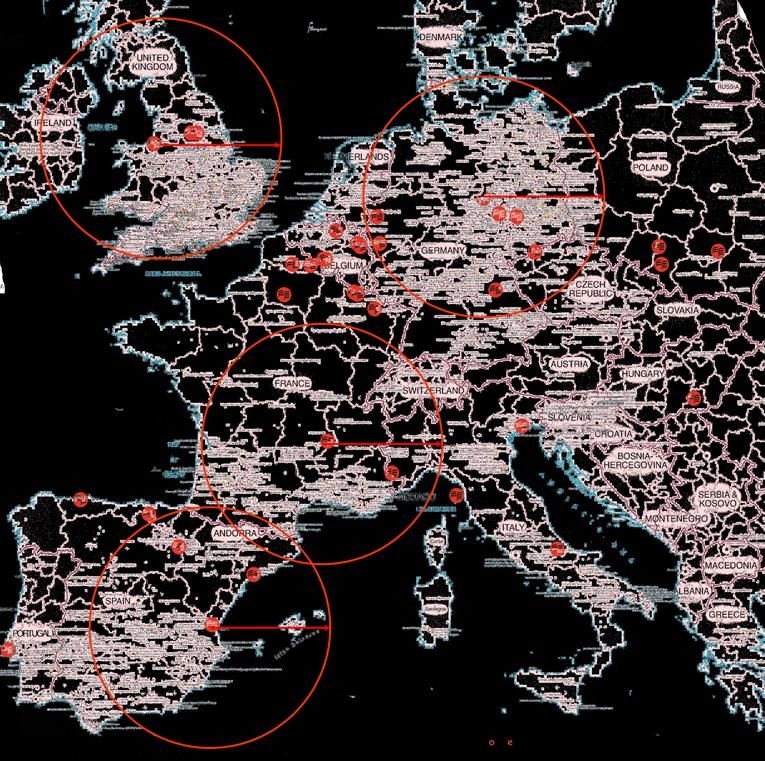
Fig. 16 illustrates examples of 500km
maximum driving distances related to
some of the major European flat glass
manufacturers (red icons).
The basic map shows the density of major
solar installations in function in 2016.
Within red circles, maximum transport
cost equal 250 €/tonne based on average
cost of 0.5 €/tkm in EU).
Figure 16: Solar PV installations (> 1.0 MW) in function in 2016*
*map is available at www.solarpowereurope.org/media/downloads
18
Cucchiella, D’Adamo and Rosa, 2015
19
PVCYCLE, 2013
Page 22 of 26CABRISS – Grant Agreement 641972 – Public Business Plan
In comparison, recycling of Si kerf is a challenging task in terms of logistics, since available quantities
are small and widely distributed. To make transport more efficient and to maintain quality and safety
standards, the kerf slurry is dried and passivated at the site of the manufacturer. Further purification
is then done at the powder production site.
The present deliverable, the project’s Public Business Plan, gives an overview of the CABRISS circular
PV value chain and connected economic aspects. More information will be presented in the
consortium’s internal intermediate and final business plans, assessing key exploitable results of the
project and their economic potential in more detail.
CABRISS strives to implement a full cradle-to-cradle PV circular economy, to exploit the challenge and
opportunity of PV wastes in Europe and globally by developing eco-efficient technologies for recycling
and reuse.
To date, CABRISS has led to a number of novel concepts for resource recycling and reuse as well as
advantages in terms of improved energy payback time and lower carbon footprint :
What is new?
✓ Economically efficient high-value recycling technology for PV panels (pilot line for thin film
panels, adapted solution for Si PV is under development): recovery of undamaged glass, silver,
silicon, indium and other rare metals.
✓ Flexible solution for recovery of silicon powders from silicon kerf.
✓ First manufacturing of targets based on secondary indium recycled from PV wastes.
✓ Reuse of recovered silver for production of conductive pastes and inks, including a resource-
saving pathway through silver-coating of copper particles.
✓ Purification of silicon to solar grade, reuse for wafer production (conventional and innovative
pathways).
✓ Cost- and resource-efficient production of ingots by hot pressing (under development).
✓ Cost- and resource-efficient production of wafers by direct thermal spraying (under
development).
✓ Novel solar cell concepts based on wafer equivalents using low-cost silicon substrates (under
development).
✓ Ongoing tests of the outputs in standard production of solar modules (thin film and Si PV).
✓ Life Cycle Analysis assessing the full cradle-to-cradle value chain available by May 2018.
Advantages
✓ Reduction of carbon footprint and EPBT
✓ Closing the loop for production of sustainable PV modules from secondary materials
✓ Reduced use of virgin silicon feedstock, silver and indium
✓ Increased eco-efficiency of solar technologies
Page 23 of 26CABRISS – Grant Agreement 641972 – Public Business Plan
2-4 N 99,00% to 99,99% purity
Al-BSF cells Aluminium (Al) back surface field (BSF) solar cell, conventional cell type in industrial
production
Amorphous- Non-crystalline form of silicon, used for a-Si solar cells and thin-film solar cells, is deposited in
Si thin films onto a variety of flexible substrates, such as glass, metal and plastic.
CdTe Cadmium Tellurite, a stable crystalline compound mainly used as semiconductor in CD
photovoltaics. The technology has low production cost, small carbon footprint and EPBT, but
is limited by toxicity of cadmium and use of rare materials (tellurium).
CIGS Copper-Indium-Gallium-Diselenid, semiconductor material which can be deposited on flexible
substrate materials, producing highly flexible, lightweight solar panels.
Crystalline-Si Crystalline silicon, the dominant semiconducting material in PV, can be multi-crystalline
(typical metal flake effect), or mono-crystalline (homogenous surface effect)
Czochralski-Si Cz-Si method of crystal growth used to obtain single crystals of semiconductors, leads to
monocrystalline Si (see above)
EPBT Energy Payback Time = defined by the relation between the energy input during the module
life cycle (manufacturing, installation, energy use during operation, and energy needed for
decommissioning) the energy savings due to electricity generated by the PV module.
EVA Copolymer between Ethylene and Vinyl Acetate, soft, flexible, “rubber-like” material with
good clarity and UV resistance.
Ingot Ingot are grown from silicon feedstock, either by melting the silicon in a crucible and letting
it cool down slowly to form a large crystal with a granular structure (multicrystalline Si) or
growth by Cz process (see above, forms a monocrystalline structure).
ITO target, Indium tin oxide (ITO) is an optoelectronic material used to produce transparent conducting
sputtering thin films by a deposition process. One of the techniques in use is sputtering. The sputtering
target target is a solid made from ITO, or from indium, and is hit by ions during the process, which
leads to the ejections of atoms from the target and deposition to the substrate.
Kerf Silicon kerf is the material which is lost as a fine powder during the process of sawing wafers
from the ingot. It is diluted in coolant liquid.
PAC Poly Aluminium Chloride, widely used flocculant in wastewater treatment, or paper industry
PERC cells Passivated Emitter and Rear Contact solar cells, alternative Si cell architecture with higher
efficiency, 10% of global c-Si cell production.
Wafer A silicon wafer is a slice of crystallised silicon (160–190 µm thick) that has been cut from an
ingot. It is the most common absorber used in PV.
WEEE Waste Electrical and Electronic Equipment Directive, the European Community directive
2012/19/EU on waste electrical and electronic equipment (WEEE) which became European
Law in February 2003. The directive set collection, recycling and recovery targets for all types
of electrical goods. Photovoltaic panels were introduced in the latest revision of 2012.
Wp The nominal power, i.e. the nameplate capacity of PV devices is measured in watt peak (or
kilowatt peak = kWp) and gives the highest power measured as output of a panel under
standardized optimum conditions.
Page 24 of 26CABRISS – Grant Agreement 641972 – Public Business Plan
Cucchiella, F., D’Adamo, I. and Rosa, P. (2015) ‘End-of-Life of used photovoltaic modules: A financial analysis’,
Renewable and Sustainable Energy Reviews. doi: 10.1016/j.rser.2015.03.076.
Cumulated energy and carbon footprint for relevant materials (retrieved June 2017) Forschungsstelle für
Energiewirtschaft München. Available at: www.ffe.de.
Fraunhofer Institute for Solar Energy Systems, I. (2016) ‘Photovoltaics Report’, (November 2016), pp. 1–43.
doi: 26.05.2014.
Indium Market by Product, ba Application, by Region and by Segment Forecasts (2016). Available at:
www.grandviewresearch.com/industry-analysis/indium-market.
IRENA_IEAPVPS_End-of-Life_Solar_PV_Panels, Report (2016).
Jäger-Waldau, A. (2016) PV Status Report 2016 October 2016. doi: 10.2790/749737.
K. Ghaffarzadeh, Y. Y. and H. Z. (2017) The Conductive Inks and Paste Business: Everything is Changing.
Osborne, Mark, P.-T. (2016) Key solar manufacturing location trends in 2016. Available at: https://www.pv-
tech.org/news/key-solar-manufacturing-location-trends-in-2016.
PVCYCLE (2013) MOBILE RECYCLING UNIT FOR PV END-OF-LIFE TREATMENT. Available at:
http://www.pvcycle.de/press/mobile-recycling-unit-for-pv-end-of-life-treatment/.
Rentzing, S. (2010) ‘Silizium-Hersteller verramschen ihre Ware’, Handelsblatt. Available at:
www.handelsblatt.com/technik/energie-umwelt/preisverfall-silizium-hersteller-verramschen-ihre-
ware/3466278.html.
SETIS Materials Information System - Indium (retrieved June 2017). Available at:
https://setis.ec.europa.eu/mis/material/indium.
The_Silver_Institute (2015) ‘Silver Scrap: The Forgotten Fundamental’, (September 2015).
Wambach, K., Schlenker, S., Müller, A. and Konrad, B. (2009) ‘A Voluntary Take Back Scheme and Industrial
Recycling of Photovoltaic Modules’, in Photovoltaics Recyling Scoping Workshop - National PV Research Center
at Brookhaven National Laboratory. Available at: https://www.bnl.gov/pv/files/PRS_Agenda/3_4_PV-Module-
RecyclingWambach.pdf.
Wild-Scholten, M. De (2011) Environmental profile of PV mass production: globalization’, 26th European
Photovoltaic Solar Energy …, (2011), pp. 2009–2012. doi: 10.4229/26thEUPVSEC2011-4DP.2.4.
Page 25 of 26You can also read