Mass Production Test of Solar Cells and Modules Made of 100% UMG Silicon. 20.76% Record Efficiency
←
→
Page content transcription
If your browser does not render page correctly, please read the page content below
Article

Mass Production Test of Solar Cells and Modules
Made of 100% UMG Silicon. 20.76%
Record Efficiency
Eduardo Forniés 1,*, Bruno Ceccaroli 2, Laura Méndez 1, Alejandro Souto 3,
Antonio Pérez Vázquez 3, Timur Vlasenko 3 and Joaquín Dieguez 4
 1 Aurinka PV Group, Marie Curie 19, 28521 Rivas‐Vaciamadrid, Madrid, Spain; lmendez@aurinkapv.com
 2 Marche and Isosilicon AS, Rognelia 30, 4622‐Kristiansand, Norway; br‐c@online.no
 3 FerroSolar, C Ucrania 6, 13500 Puertollano (Ciudad Real), Spain; asouto@ferroglobe.com (A.S.);
   anpervaz@ferroglobe.com (A.P.); tvlasenko@ferrosolar.com (T.V.)
 4 Ferroglobe, 15142 Arteixo‐La Coruña, Spain; jdieguez@ferroglobe.com
 * Correspondence: efornies@aurinkapv.com

 Received: 2 April 2019; Accepted: 17 April 2019; Published: 19 April 2019

 Abstract: For more than 15 years FerroAtlantica (now Ferroglobe) has been developing a method of
 silicon purification to obtain Upgraded Metallurgical Grade Silicon (UMG‐Si) for PV solar applica‐
 tion without blending. After many improvements and optimizations, the final process has clearly
 demonstrated its validity in terms of quality and costs. In this paper the authors present new results
 stemming from a first mass‐production campaign and a detailed description of the purification pro‐
 cess that results in the tested UMG‐Si. The subsequent steps in the value chain for the wafer, cell
 and module manufacturing are also described. Two independent companies, among the Tier‐1 solar
 cells producers, were selected for the industrial test, each using a different solar cell technology: Al‐
 BSF and black silicon + PERC. Cells and modules were manufactured in conventional production
 lines and their performances compared to those obtained with standard polysilicon wafers pro‐
 duced in the same lines and periods. Thus, for Al‐BSF technology, the average efficiency of solar
 cells obtained with UMG‐Si was (18.4 ± 0.4)% compared to 18.49% obtained with polysilicon‐made
 wafers. In the case of black silicon + PERC, the average efficiency obtained with UMG‐Si was (20.1
 ± 0.6)%, compared to 20.41% for polysilicon multicrystalline wafers.

 Keywords: solar cells; UMG silicon; purification; PERC; black silicon

1. Introduction
     Photovoltaics has for long clearly demonstrated its ability to be a competitive source of electric‐
ity. Measured in terms of Levelized Cost of Electricity (LCOE), photovoltaic power plants appear far
more competitive than either fossil or other renewable energies (Figure 1).
      To achieve this, many contributions have been necessary along the whole value chain combining
cost reduction and increase of efficiency. Thanks to drastic cost reductions and massive capacity
expansion over years, the silicon material which accounts for 20–24% of the PV module cost (in Figure
2, sum of blue and green slices), contributes largely to keep crystalline silicon in the lead of PV
technologies. The UMG‐Si used in this test has incidence in the green slice (convers. Me‐Si to Si‐So)
of Figure 2.

Energies 2019, 12, 1495; doi:10.3390/en12081495                              www.mdpi.com/journal/energies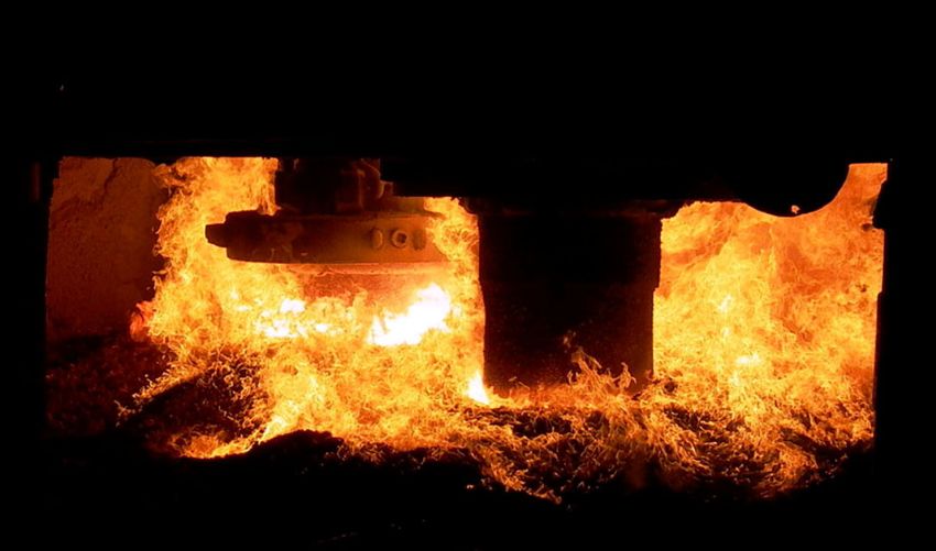
Energies 2019, 12, 1495 2 of 16
Figure 1. Levelized Costs of Electricity. Renewable Energy Technologies. March 2018. Fraunhofer
ISE [1]. FLH in h/a refers to the annual full load hours per annum.
Figure 2. Module cost breakdown. Includes all the costs (cash costs, SG&A expenses and depreciation)
except for the Me‐SiG where only the material price is included. Me‐Si stands for metallurgical grade
silicon and Si‐So for solar grade silicon.
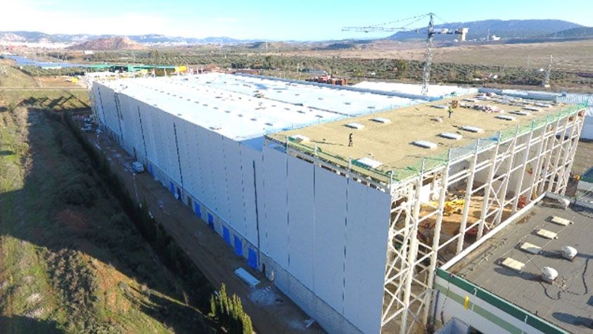
After years of development, FerroGlobe has decided, under the name of FerroSolar OpCo, to
move to industrial scale for producing UMG silicon (UMG‐Si) for solar applications. A new factory
is currently being built in Puertollano (Spain) with a capacity of 3000 t/year (Figure 3). This factory
will deploy a process concept developed through many years while adding new recent improve‐
ments that will help to further reduce the cost and improve the quality. The aim of this factory of
moderate output capacity is to become the basic unit and platform to further grow up to the Gigawatt
level, and further decrease the cost through economy of scale.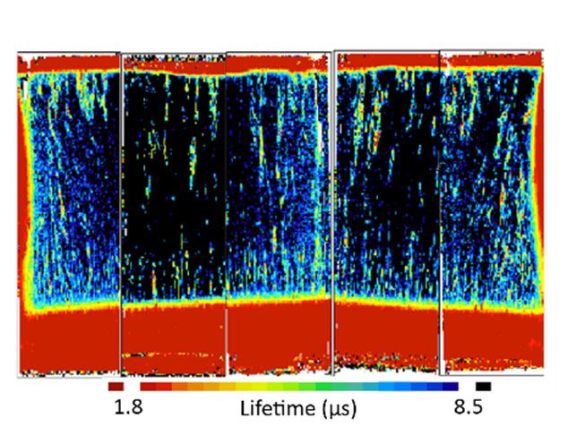
Energies 2019, 12, 1495 3 of 16
Figure 3. UMG‐Si production factory at Puertollano (Spain).
Aurinka PV Group, the engineering team that has been developing the industrialization of the
project, has created a simulation software specific for the purification process, that, together with the
inputs of every single data from all the steps of the overall process, is able to provide the cash costs
for different scenarios. In that way, the consumption of electricity, manpower, consumables, spare
parts, etc., are considered. As it is a “real time” software, the lag of every single machine shows up
as a natural consequence of the eventual lack of simulated resources (operators, forklifts, furnaces,
etc.). Then the uptime is well calculated, and the optimal number of resources assessed to minimize
the cash cost and maximize the productivity. By means of that software and the optimization of the
process, the cash cost of a large‐scale factory has been calculated to be below 7 $/kg, being price of
electricity and manpower cost considered for Spanish location.
It is already well established that the UMG‐Si produced by the mentioned process can be utilized
100% in the charge to multicrystalline ingots growth, without the need of mixing with polysilicon.
Several tests have also been done in single crystal (monocrystalline) growing using 100% UMG‐Si
with good results. However, such tests have not been brought to mass production yet. UMG‐Si, be‐
cause of its low cost and physical characteristics, has the potential to keep multicrystalline in the
competitive race with the other PV technologies including the most recently fast‐growing single crys‐
tal and keep a notable share of the market.
To illustrate this competition between the two major crystalline silicon technologies, it will be
explained, in the following discussion, recent technology developments and implementations which
are contributing to their respective success:
Diamond‐Wire Saw (DWS), introduced to the market gradually during the past 5 years, is con‐
sidered a disruptive wafer sawing technology due to its lower costs of ownership and the higher
throughput (around 60 wafers per kg of certified silicon) compared to traditional Slurry Cut
Wire Saw (SWS). Nevertheless, while those advantages have been applied effectively to mono‐
crystalline ingots, the throughput for multicrystalline has been slightly less (around 55 wafers
per kg) than in mono. Moreover, the multicrystalline technology has suffered from problems of
texturization due to the soft wafer surface resulting from the DWS.
PERC: The implementation of high efficiency cell architectures as Passivated Emitter and Rear
Cell has also adversely affected the multicrystalline technology variant. Due to the optimization
of surface passivation of the cells, the bulk lifetime, lower in multi than in mono, has become the
limiting factor of cell efficiency.
LeTID or CID: The Light at elevated Temperature Induced Degradation (LeTID) or the Current
Induced Degradation (CID) has become a deleterious effect on multicrystalline PERC solar cells.
It results in a deep degradation of performance of the module once installed in real outdoor
conditions [2]. Boron oxide complexes (B‐O) or iron boron pairs (FeB) cannot be considered re‐
sponsible for LeTID or CID, as they are for Light Induced Degradation (LID). It is currently as‐
sumed that hydrogen introduced for passivation plays an important role in this degradation [3].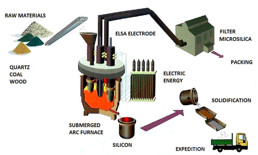
Energies 2019, 12, 1495 4 of 16
Nevertheless, several technology steps have recently proven to be effective countermeasures
that minimize or even eliminate these adversely effects. Among those are extended phosphorus
diffusion gettering (ePDG), black silicon (B‐Si), mono‐like crystallization and current induced
recovery (CIR):
ePDG: Phosphorus diffusion gettering happens naturally during the emitter diffusion step of
the conventional p‐type cell process flow, improving the bulk minority carrier lifetime signifi‐
cantly. Since the 1970s, phosphorus doping is done at industrial level using POCl3 thermal dif‐
fusion [4]. The main advantages of this technology are the low operational costs and the com‐
mercial readily availability of high‐throughput equipment. Normally, phosphorus diffusion is
carried out in two steps, first a phosphosilicate glass (PSG) layer is deposited on the surface of
the wafer and afterwards the phosphorus is forced to move deeper in a drive‐in step, which is
carried out at a lower temperature and without the feeding of the phosphorus source. The im‐
purity gettering happens in the phosphorus diffusion and other thermal steps of cell processing,
such as passivation [5], low thermal annealing (LTA) or contacts co‐firing [6]. This phenomenon
is responsible for the better bulk lifetime and emitter recombination properties of the processed
material when compared to the as‐grown material. Nevertheless, it is a complex phenomenon
in which several competing mechanisms take place [7], including internal impurities gettering
(migration to grain boundaries, dislocation or precipitates), external impurities gettering (mi‐
gration to the surface), defects reconfiguration or bulk passivation of defects or changes in the
surface recombination velocity (by hydrogen for example, during SiNx layer formation). In the
case of UMG‐Si, and other solar grade materials obtained by metallurgical purification, the pres‐
ence of impurities, especially iron, is higher than in a p‐type multicrystalline silicon made from
polysilicon. This element is mainly present in the form of interstitial iron and can be significantly
reduced by the application of tailored process parameters [8,9], without increasing neither the
overall cost nor the complexity of the operations. In our case an “extended” PDG (or ePDG)
should be used, encompassing engineering intervention in all the thermal processes during solar
cells production in addition to phosphorus diffusion.
B‐Si: Black silicon is being introduced in a massive scale into production lines [10]. Due to the
reduction of reflection, B‐Si has been able to increase the absolute efficiency of multicrystalline
solar cells up to 0.4 %abs [11]. Moreover, according to Pasanen et al. [12], both PDG and B‐Si
techniques in combination, have additive and synergetic effects that potentiate each other, open‐
ing the possibility of using metallurgically refined silicon to high efficiency solar cells. The com‐
bination of B‐Si and PDG together with the usage of high‐quality silicon purified by metallurgi‐
cal route, also known as upgraded metallurgical grade silicon (UMG‐Si), can contribute to lower
production cost of PV ($/kWp). Pasanen et al. have also published the positive impact of B‐Si on
solar cells in terms of Current Induced Degradation, which emphasizes even more the possibil‐
ities of UMG‐Si [3]. Under an economical assessment, Modanese et al. [13] calculated a relative
cost reduction of up to 11.7% for a multicrystalline B‐Si + PERC solar cell compared with a mono‐
crystalline PERC solar cell, being most of the reduction related to feedstock and ingot growing.
LeTID recovery or current induced recovery (CIR): There are several techniques that can miti‐
gate or even eliminate the LeTID or CID of the cells. Most of these consist in applying tempera‐
ture, current or light [14–16]. In fact, CIR has been already tested industrially and implemented
successfully in productions lines. This method accelerates the LeTID, that typically takes thou‐
sands of hours, and provokes the final recovery of the solar cells that would otherwise takes
place naturally in the field only after several months.
Mono‐like: This silicon growth technology was already introduced in the industry in 2012 [17]
with good results in terms of quality, but suffered of structure inhomogeneity along the ingot
height. This, together with the cost of the seeds and the rapid and successful introduction of the
high performance multicrystalline (HPM) growth technique, kept the mono‐like (also called
mono‐cast) out of the business. Nevertheless, companies among the PV leaders are currently
revisiting and adopting this technology [18], indicating that the previous drawbacks can be over‐
come.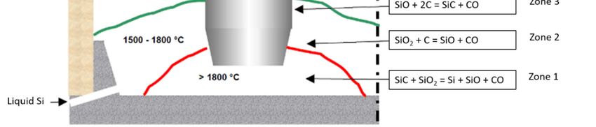
Energies 2019, 12, 1495                                                                          5 of 16

     For all these reasons mentioned above, it is believed that the multicrystalline wafers can stand
the boost of mono and keep a high market share in the future. That was one of the conclusions of the
last EU PVSEC [19]. High quality UMG‐Si can contribute to this, not only because of the lower pro‐
duction costs, but also because of lower energy budget (around 30 kWh/kg), lower specific Capex
(15‐30 $/kg, depending on the capacity) and lower carbon footprint.
      In the next sections of this paper the process steps followed to accomplish the test will be ex‐
plained in detail, starting from the MeG‐Si production and finishing with the module production and
characterization. This is the occasion to give a detailed description of the UMG‐Si process as it is
under construction at the Puertollano plant. The whole test, from silicon purification to module pro‐
duction, was inspected by TÜV Rheinland [20] (for more details see Results and Discussion below).

2. Materials and Methods

2.1. Carbo‐Reduction to Obtain MeG‐Si
    The fabrication process for metallurgical silicon is the carbo‐reduction of quartz by coal in a
submerged electrode arc furnace according to the reaction:
                                              SiO2 + 2C = Si + 2CO                                  (1)
      The silicon production furnace is a crucible of about 10 m in diameter and 3 m deep lined with
refractory material, powered by a three‐phase electrode system. The furnace has many auxiliary fa‐
cilities around as depicted in Figure 4.

                          Figure 4. Me‐Si production furnace and auxiliary facilities.

      In a continuous process, the furnace is loaded with raw materials and the resulting liquid metal
is tapped continuously. Silicon’s melting point is 1415 °C. The charge is heated up to a temperature
around 2000 °C by means of three electrodes submerged in the raw material mixture (Figure 5),
providing three‐phase current. At these temperatures the reduction of silica occurs, resulting in metal
silicon. The molten silicon poured out from the reaction vessel is subsequently refined by slag treat‐
ment or gas purge. During the refining, oxide and carbide particles are removed, adjusting the metal
composition.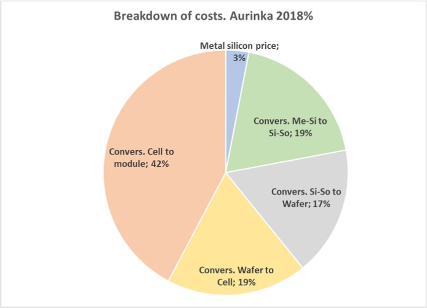
Energies 2019, 12, 1495                                                                                   6 of 16

      Figure 5. Picture of the upper part (zone 5, Figure 6) of a submerged ARC electrode furnace during
      process showing two electrodes in the center of the picture.

      After refining, the melt is poured for solidification, cooled down, crushed and milled. The elec‐
trical power consumption is about 11–13 MWh per ton of silicon produced in state‐of‐the‐art pro‐
cesses. Excess energy provided by the furnace and not consumed in reaction (1) (3–5 MWh/t of sili‐
con) can be reclaimed in a heat recovery station or used to produce electricity in a cogeneration plant.
The overall reaction as expressed in Equation (1) is, in fact, the summary of several steps [21]. When
heating, volatiles from carbon are removed upwards and the quartz goes down with carbon into the
oven. In the inner zone (zone 2, Figure 6).

        Figure 6. Sketch of the electrode and different zones inside a submerged ARC electrode furnace.

      SiO is generated according to:
                                              SiO2 + C = SiO + CO                                            (2)
    The generated gaseous and unstable (metastable) SiO rises to an intermediate height (zone 3)
and reacts with more C to give SiC according to:
                                              SiO + 2C = SiC + CO                                            (3)
    The SiC descends to the hot zone of the oven (zone 1; Figure 6) and with remaining quartz
generates Si: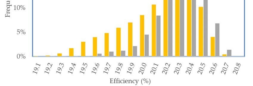
Energies 2019, 12, 1495 7 of 16
SiC + SiO2 = Si + SiO + CO (4)
For the good performance of the oven, it is critical to capture the generated CO, otherwise the
yield of the furnace decreases significantly. To recover this CO there is only one mechanism, in the
upper part of the oven (zone 4):
SiO + CO = SiO2 + C (5)
The product is traditionally called silicon metal or metallurgical grade silicon MeG‐Si. The chem‐
ical characteristics of the MeG‐Si traded in the market, fall within the following ranges:
Metals (principally Fe, Al, Ca followed by Ti, Mn and traces of transition metal): 1 to 4%
Boron: 8–50 ppmw
Phosphorus: 10–50 ppmw
Aluminum and calcium content can be significantly reduced by oxidation in the refining ladle
(slag or gas treatment—see above) while the level of iron and the other transition metals depend
ultimately on the purity of the quartz and the type of coal used. It is possible to mix several types of
quartz and reductants in the feeding charge to tailor the final composition of the metallurgical grade
silicon (with less than 0.2% ppmw of impurities) more suitable as starting point of the purification
process.
2.2. Silicon Purification
For photovoltaic purposes, the MeG‐Si must be purified either by direct (metallurgical treat‐
ment) or indirect (chemical treatment) route [22]. Regarding the FerroSolar UMG process, MeG‐Si
has been used as a starting material. As mentioned in the previous section, the characteristics of MeG‐
Si are established standards in the market. An oversimplified description of the process selected by
FerroSolar is depicted in Figure 7.
Figure 7. Descriptive sketch of the purification process at FerroSolar.
2.2.1. Slagging
Silicon produced through carbothermic reduction of quartz contains about 99% of Si, with Fe,
Al, Ca, Ti, C and O being the most common impurities. The less noble elements, e.g. Al and Ca, can
be significantly removed by oxidation (see refining of MeG‐Si above). Fe and the transition elements
are not affected by oxidation. These can be efficiently removed by directional solidification (DS),
which also impacts, although to a lesser degree, to other elements. Boron and phosphorus are present
in tens of ppmw in MeG‐Si. Since these elements are respectively p and n silicon dopants, they must
be closely controlled in solar grade silicon. Unfortunately, both impurities are difficult to remove by
traditional purification routes such as directional solidification or acid leaching, due to their large
segregation coefficients KB = 0.8 and KP = 0.35 [23]. Therefore, several alternative methods have been
studied and developed to remove boron such as slag refining [24,25] plasma refining [26], and gas
refining [27,28].
Slag refining is well established in many metallurgical processes and can be operated on a large
industrial scale. This represents a great advantage over other boron removal methods that are not
easily scalable. Most of the known slag‐forming composition include binary, such as CaO‐SiO2, ter‐
nary CaO‐Al2O3‐CaO, CaO‐MgO‐SiO2, CaO‐Na2O‐SiO2, Al2O3‐BaO‐SiO2, and even quaternary com‐
positions as Al2O3‐CaO‐MgO‐SiO2 [29].
In slag refining, metallurgical grade silicon is melted in contact with a slag‐forming compound.
In case of boron the basic principle of slag purification is the oxidation of boron at the Si/Slag interface,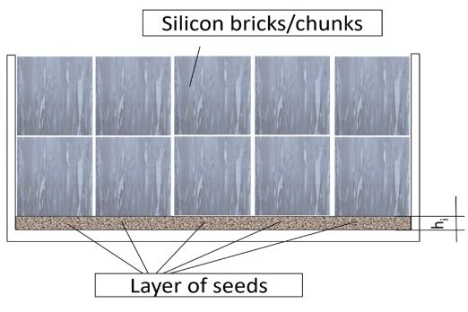
Energies 2019, 12, 1495 8 of 16
followed by the dissolution of the oxidized boron in the slag phase. B as impurity to silicon can be
oxidized to BO, B2O, B2O3, BO2, and B2O2(g). Thermodynamics of boron removal with slags have been
studied in great detail. Most of these studies focused on the calculation and optimization of the equi‐
librium conditions between Si and slag. In general, the efficiency of boron removal from silicon is
increased with increasing temperature and with slag basicity. Depending on slag composition, boron
removed from silicon can remain concentrated in the slag or volatilized to the atmosphere as gaseous
compounds. The general principle for plasma refining and gas refining is essentially the same, oxi‐
dation of boron to gaseous compounds at high temperature, and volatilization of said compounds to
the atmosphere. The first step of this UMG process includes a reactive slagging treatment, capable of
decreasing boron content in silicon to below 0.2 ppmw.
2.2.2. Vacuum Refining
As mentioned above, a major challenge in silicon purification through metallurgical routes is the
removal of phosphorus. Vacuum refining can be considered as an alternative purification route in
which the volatile impurities, such as phosphorus, are effectively removed.
From a thermodynamics point of view, the principle of an effective removal of impurities from
a liquid metal under vacuum at elevated temperature is the difference of the respective vapor pres‐
sure between the metal to be refined and the impurities. According to this approximation, dissolved
impurities with higher vapor pressure than silicon are expected to evaporate away.
Thermodynamics alone is not enough, since the evaporation of an impurity may be too slow to
proceed practically. Therefore, the evaporation of phosphorus must be studied also from a kinetic
point of view. Depending on experimental conditions, phosphorus evaporates as P4(g), P2(g) and P(g).
In metallurgical grade silicon, evaporation as P(g) becomes dominating at concentrations of phos‐
phorus below 50 ppmw and high temperatures [30,31]. Under these conditions, evaporation follows
a first order reaction:
P P i exp K p A
t (6)
V
where [P] and [P]i are, respectively, the final and initial phosphorus concentration in silicon, A is the
surface area of the melt (m2), V is the volume of the melt (m3), Kp is the evaporation rate constant (m/s)
and t is the time (s). Detailed studies on reaction mechanism concluded that the removal of phospho‐
rus from silicon occurs through five steps: (i) transport of phosphorus close to the surface of the melt;
(ii) transport of phosphorus to the surface through the interface layer; (iii) evaporation at the melt
surface; (iv).‐ mass transport of gaseous phosphorus and (v): condensation of phosphorus [32,33].
Several silicon recycling treatments under vacuum at high temperatures have been conducted
during the last few years at FerroSolar´s pilot plant in Sabon (Spain), in a graphite resistance furnace
[34]. 490 kg of silicon with a starting phosphorus concentration of 3 ppmw were treated in each run,
in high density isostatic graphite crucibles. The goal of these experiments was to check the influence
of experimental parameters on the efficiency of phosphorus removal. Internal pressure in the furnace
was maintained in the range 0.1–0.3 Pa throughout the treatment. As a result of these vacuum treat‐
ments, concentration of phosphorus in purified silicon was in the range of 0.1–0.2 ppmw, and mass
transfer coefficients of up to 7×10⁻⁵ m/s.
As expected, increasing treatment temperature resulted in increased evaporation rates. Process
temperature has been stabilized within the range 1600–1700 °C. Although higher temperatures lead
to faster evaporation rates, they would have a detrimental effect on the lifetime of the different com‐
ponents of the furnace, thus a compromise between temperature and process time has been reached
to optimize the production costs, in which the lifetime of the components have been also considered
in the calculation. These results are in good agreement with the kinetic model in which phosphorus
removal rate is controlled by the reaction at the interface and the mass transport in the gas phase.
2.2.3. Directional Solidification
Energies 2019, 12, 1495                                                                                9 of 16

      Directional solidification is an essential step to obtain solar grade silicon. The basis of the process
is the equilibrium established between the concentration of an impurity in the solid and liquid silicon.
As a consequence of the general tendency of impurities to concentrate in liquid silicon, high purity
solid silicon is obtained in an economical feasible way.
      Segregation of each impurity is given by its own segregation coefficient, which is the ratio be‐
tween the equilibrium concentrations of the element in solid and liquid silicon. The lower the coeffi‐
cient, the better the purification. Most of the impurities in silicon have segregation coefficients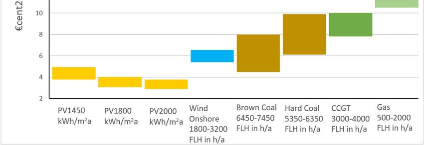
Energies 2019, 12, 1495 10 of 16
(a) (b)
Figure 8. (a) Sketch of the charge of the directional solidification furnace. Crucible dimensions: 890
890 540 mm, layer of seeds hi = 50 mm; (b) Lifetime mapping of a representative ingot.
2.4. Solar Cells Production
2.4.1. Al‐BSF Cells
Approximately 100,000 wafers were sent to a Tier‐1 solar cells producer, also responsible for
module manufacturing. The wafers, after passing the initial incoming material inspection, were in‐
troduced into the production line.
Aluminum Back Surface Field (Al‐BSF) solar cells were produced in a conventional production
line, where no adjustment was made for adjusting the production parameters of the machines to the
peculiarities of the incoming UMG‐Si wafers. So, it is reasonable to expect a certain improvement of
efficiency and yield in case the recommendable fine‐tuning of the line to a new provider would be
performed. The process is depicted in Figure 9, and consists of the following steps:
1. The first stage consists in a nitric and hydrofluoric acid etching for surface cleaning, saw damage
removal and texturing.
2. The wafers are placed back to back to be introduced into quartz furnaces to perform a Low Pres‐
sure Chemical Vapor Deposition (LPCVD) of a thin film of phosphosilicate glass (PSG) com‐
posed of (P2O5)x(SiO2)1‐x.
3. In the next step the diffused phosphorus from the back side is removed. For that, a back side
chemical etching is performed, followed by a rinse in another chemical etching to achieve the
edge isolation and avoid the edge shunts.
4. Annealing is a pre‐treatment process prior to antireflective coating (ARC) of silicon nitride. In
this short process a thin film of silicon dioxide is deposited to increase the Potential Induced
Degradation resistance of the solar cell, what is commercially called PID free solar cells [37].
5. Antireflective Coating (ARC). Silicon nitride (SiNx:H) coating of approximately 75nm thick is
deposited on the front surface by means of a Plasma Enhanced Chemical Vapor Deposition re‐
actor (PECVD) to increase light absorption. This coating is also suited for surface passivation
due to the field effect passivation [38]. The Hydrogen present in the silicon nitride coating is also
involved in a chemical passivation [39].
6. Front and rear contacts as well as the Aluminum coating responsible for the Back Surface Field
(BSF) formation are printed in a double printing process, saving Ag consumption and reducing
the shadow losses [40].
7. Co‐firing furnace is used to make the drive through of the contacts [41].
8. In the last step of the solar cells production, the solar cells undergo an electroluminescence test
(EL test) [42] where a defect detection software is used.Energies 2019, 12, 1495 11 of 16
Figure 9. Descriptive sketch of Al‐BSF solar cells production.
2.4.2. Black Silicon + PERC Cells
45,000 wafers (DWS) were sent to another and independent solar cell producer. The technology
used in this case was black silicon + PERC as depicted in Figure 10.
Besides the common production steps of Al‐BSF process, mentioned above, the following addi‐
tional processes are introduced to obtain black silicon + PERC solar cells:
2) Black silicon (B‐Si) nano‐texture. The technology used to provoke a nano‐texture on top of the
wafer is reactive ion etching (RIE). SF6 and O2 gases are introduced into the reaction chamber. In
there, a synergetic mechanism of chemical etching, passivation and ion bombardment takes
place, thus, nano‐structures are formed reducing considerably the reflectance of the wafer
[10,43].
6) Back surface passivation. To reduce the back surface recombination a passivation layer is de‐
posited in the back surface which gives name to the passivated emitter and rear cells (PERC)
[44,45]. In this test, an Al2O3 film is deposited onto the back surface, acting as a passivating agent.
After the oxide deposition, a capping layer of silicon nitride was deposited. The role of this cap‐
ping layer is to behave as a back reflector for long wavelength radiation as well as being a barrier
for Al metal contacts. Also, this silicon nitride reduces the surface recombination velocity due to
its negative charge [46]. Both films were deposited by means of PECVD.
8) Laser Contacts Opening. Backside openings through the passivation stack were made by a
nanosecond pulsed laser.
9) To minimize the light at elevated temperature degradation (LeTID) [14–16] a post‐treatment
of the cells is performed.
Figure 10. Descriptive sketch of B‐Si + PERC solar cells production.
3.5 PV Modules Production
The modules manufacturing has followed a standard production process (Figure 11). The same
bill of materials (BOM) and production line were used for both, UMG‐Si and polysilicon solar cells.Energies 2019, 12, 1495 12 of 16
Figure 11. Descriptive sketch PV module production.
3. Results and Discussion
After several tests at a small production scale with good results [47], a mass production test was
performed with the solar silicon generated in its direct purification process. For that, several tons of
silicon were used to grow multicrystalline HPM silicon. Then the wafers were sent to two different
Tier‐1 solar cell and module producer, where both Al‐BSF and B‐Si + PERC modules were produced.
The results of the cells and modules had to be compared with those obtained with polysilicon base
material. For sake of external and independent audition, all the production steps throughout the
whole value chain, from silicon purification to module production, were inspected by the TÜV
Rheinland. One inspector from TÜV has been accompanying the technicians in all the production
lines to check the production of the material and that the incoming raw material of one production
line were the same that outwent from the previous production line. Thus, the whole process and
material tracking was certified by an external auditor [21].
Since different companies have different cell to module losses (CTM losses) depending on the
bill of materials (BOM), module design and manufacturing procedure [48,49], only the solar cells
results will, in the following, be compared with those obtained with polysilicon. In any case, as an
example, the average module performances are reported in Table 1 (only data for 72 cells modules
are shown).
Table 1. Average values of module production.
Pmax Voc Isc Vmpp Impp FF
Cell Technology Counts
[W] [V] [A] [V] [A] %
Black silicon+ PERC 354.4 47.48 9.70 38.21 9.28 77.00 300
Al‐BSF 325.1 45.73 9.32 37.13 8.76 76.31 1350
As it is shown in Table 2, the highest efficiency was obtained with B‐Si + PERC (as expected).
The average efficiency is (20.4 ± 0.6) % and the record efficiency 20.76 % (not shown in the table). As
previously emphasized, no tune of parameters of production lines was done to perform these tests.
Table 2. Average values of solar cells production. Comparison between polysilicon and UMG‐Si. The
dashes in the cells stand for data not given by the producer. Column Red.%rel refers to relative reduc‐
tion in efficiency between UMG and poly.
Pmpp Voc Isc Red. Umpp Impp Rsh
Solar Cells Results FF % Eta % Counts TEST
[W] [V] [A] %rel [V] [A] [Ω]
UMG 4.549 0.632 9.03 79.74 18.515 0.535 8.501 141 2,000 TEST
Al‐BSF 0.68% 1[1]
Poly 4.579 0.634 9.06 79.69 18.642 ‐‐‐‐‐‐‐‐‐ ‐‐‐‐‐‐‐‐‐ 131 ‐‐‐‐‐‐‐‐
Prod.A
UMG 4.522 0.632 9.02 79.27 18.404 0.533 8.487 86 99,692 TEST 2
Al‐BSF 0.47%
Poly 4.543 0.633 8.98 79.63 18.490 ‐‐‐‐‐‐‐‐‐ ‐‐‐‐‐‐‐‐‐ 112 ‐‐‐‐‐‐‐‐ Prod.A
B‐Si (RIE) + UMG 4.945 0.649 9.54 79.87 20.130 0.550 8.994 279 46,197 TEST 3
1.37%
PERC Poly 5.014 0.651 9.62 80.02 20.410 ‐‐‐‐‐‐‐‐‐ ‐‐‐‐‐‐‐‐ 508 55,396 Prod.B
Considering that UMG Solar Grade Silicon is a new material on the market and characteristics
are somehow different from the main stream silicon feedstock (mainly the dopants concentration),
the authors consider these results to be very encouraging. Similar tests were carried out with the same
silicon but using only metal catalyzed chemical etching (MCCE) nano‐texturization [50], but to theEnergies 2019, 12, 1495 13 of 16
best of our knowledge, the present results show a record efficiency for p‐type multicrystalline UMG‐
Si solar cells. Moreover, the yield, in terms of breakage and rejection, is the same for both type of
materials (polysilicon and UMG‐Si).
Considering the comparison with polysilicon material, for which Grade I solar silicon (according
SEMI PV17‐0611 2011 classification) has been used (B < 0.00038 ppmw, P < 0.00110 ppmw), the mass
production test with Al‐BSF gives a loss of power of 0.68%rel less than the power obtained with pol‐
ysilicon wafers. In the case of B‐Si + PERC the loss of power is higher, 1.37%rel. This is in concordance
with the architecture of cell used. In PERC solar cells, due to the back surface passivation, the surface
recombination velocity is considerably reduced, thus the bulk lifetime becomes a more influencing
parameter than in the case of Al‐BSF solar cells [51]. UMG‐Si material, although inside specifications,
is expected to contain more contaminants than polysilicon. So, the bulk lifetime, in average, is likely
to be lower in UMG‐Si PERC solar cells. Lower bulk lifetime is translated into lower Voc, which is
the case for this silicon. However, the Voc for UMG cells is only 0.38%rel less than that for polysilicon
cells. Meanwhile Isc is almost 1%rel lower, which suggests a detrimental effect more related to light
trapping (B‐Si or ARC processes) than to bulk lifetime. Moreover, Bredemeier et al. [14], in their
LeTID study of the recovery, conjectured that the “regeneration conditions need to be adapted to the
mc‐Si used”. All of this makes more important the tuning of the production parameters to enhance
impurity gettering, bulk defects passivation and light trapping in UMG‐Si solar cells.
In Figure 12 the efficiency distribution of solar cells is shown. In case of solar cells made of UMG‐
Si the left tail of the distribution is more pronounced than in polysilicon. This tail contributes to re‐
duce the average down to 20.1%. However, the distribution presents the same mode both, for cells
made of UMG‐Si and polysilicon. Thus, working on defects engineering, passivation and production
parameters, the average efficiency of UMG‐Si can therefore be at par with polysilicon.
Figure 12. Distribution of efficiencies for solar cells B‐Si + PERC. Comparison between polysilicon and
UMG‐Si.
This paper has presented a mass production test that involves the whole value chain from quartz
mineral to PV in field module. The material traceability from purification to modules was carried out
and certified by TÜV Rheinland. The results of the test in terms of yield and electrical parameters are
close to polysilicon. To keep improving the performance, the research should continue in different
directions:
At the purification level, several improvements are being developed at the laboratory scale.
Management, valorization and recycling of byproducts such as silicon fines, silica, etc. are giving
auspicious results. Another important step forward is the promising results in the increasing of the
throughput and the reduction of energy budget.Energies 2019, 12, 1495 14 of 16
At the cell level, ePDG, Black Silicon and passivation are being studied. Aurinka and FerroSolar
are involved in a project with other research institutions to apply these techniques to our silicon and
other potential UMG‐Si. Parameters such as surface roughness, PSG conformality, phosphorus diffu‐
sion temperature, drive‐in time, co‐firing temperature, etc., must be very well matched in order to
achieve the best performance.
Module degradation (after more than 3 years of outdoors operation [52]) and temperature coef‐
ficients [53] have been already studied. The modules made of UMG‐Si showed no additional degra‐
dation compared with polysilicon modules, meanwhile the power thermal coefficient of modules
made of UMG‐Si resulted to be lower than that of polysilicon modules. Further studies are being
carried out with modules resulting from this manufacturing test. So far only data for Al‐BSF modules
is available: after one 46 days of outdoors installation, modules made of UMG‐Si showed similar
degradation than those made of polysilicon. FerroSolar will continue to monitor all multicrystalline
modules produced in the test and further work will be carried out on single‐crystal growing with
100% UMG silicon usage.
Author Contributions: Conceptualization, E.F.; methodology, E.F., B.C., L.M., A.S., A.P.V.; validation, E.F., B.C.;
formal analysis, E.F.; investigation, E.F., T.V., J.D.; resources, E.F, L.M., A.S., A.P.V.; data curation, E.F., J.D.;
writing—original draft preparation, E.F., L.M., T.V., A.S., A.P.V.; writing—review and editing, E.F., B.C., L.M..;
visualization, E.F.; supervision, E.F., B.C.; project administration, E.F.; funding acquisition, E.F.
Funding: This research received no external funding.
Conflicts of Interest: The authors declare no conflict of interest
References
1. Kost, C.; Shammugam, S.; Jülch, V.; Nguyen, H.‐T.; Schlegl, T.; Mayer, J.N.; Thomsen, J.; Hartmann, N.;
Senkpiel, C.; Philipps, S.; et al. Levelized Cost of Electricity: Renewable Energy Technologies; Fraunhofer ISE:
Freiburg, Germany, 2018.
2. Kersten, F.; Engelhart, P.; Ploigt, H.‐C.; Stekolnikov, A.; Lindner, T.; Stenzel, F.; Bartzsch, M.; Szpeth, A.;
Petter, K.; Heitmann, J.; et al. Degradation of multicrystalline silicon solar cells and modules after
illumination at elevated temperature. Sol. Energy Mater. Sol. Cells 2015, 142, 83–86.
3. Pasanen, T.P.; Modanese, C.; Vähänissi, V.; Laine, H.S.; Wolny, F.; Oehlke, A.; Kusterer, C.; Heikkinen,
I.T.S.; Wagner, M.; Savin, H. Impact of black silicon on light‐ and elevated temperature‐induced
degradation in industrial passivated emitter and rear cells. Prog. Photovolt. Res. Appl. 2018,
doi:10.1002/pip.3088.
4. Li, H.; Kim, K.; Hallam, B.; Hoex, B.; Wenham, S.; Abbott, M. POCl3 diffusion for industrial Si solar cell
emitter formation. Front. Energy 2017, 11, 42–51.
5. Hallam, B.; Chen, D.; Kim, M.; Stefani, B.; Hoex, B.; Abbott, M.; Wenham, S. The role of hydrogenation and
gettering in enhancing the efficiency of next‐generation Si solar cells: An industrial perspective. Phys. Status
Solidi Appl. Mater. Sci. 2017, 214, 1700305.
6. Peral, A.; Dastgheib‐Shirazi, A.; Fano, V.; Jimeno, J.C.; Hahn, G.; del Canizo, C. Impact of Extended Contact
Cofiring on Multicrystalline Silicon Solar Cell Parameters. IEEE J. Photovolt. 2017, 7, 91–96.
7. Al‐Amin, M.; Murphy, J.D. Passivation effects on low‐temperature gettering in multicrystalline silicon.
IEEE J. Photovolt. 2017, 7, 68–77.
8. Jiménez, A.; del Cañizo, C.; Cid, C.; Peral, A. Phosphorus Diffusion Gettering Efficacy in Upgraded
Metallurgical‐Grade Solar Silicon. J. Electron. Mater. 2018, 47, 5068–5071.
9. Kohler, D.; Raabe, B.; Braun, S.; Seren, S.; Hahn, G. Upgraded metallurgical grade silicon solar cells : A
detailed material analysis. In Proceedings of the 24th European Photovoltaic Solar Energy Conference,
Hamburg, Germany, 21–24 September 2009; pp. 1758–1761.
10. Rentsch, J.; Kafle, B.; Hofmann, M.; Krieg, K.; Zimmer, M. Texture etching technologies for diamond‐wire‐
sawn mc‐Si solar cells. Photovolt. Int. 2017, 38, 56–66.
11. Wang, X.; Zou, S.; Xing, G. 19.31%‐efficiency multicrystalline silicon solar cells using MCCE black silicon
technology. Photovolt. Int. 2017, 35, 67–72.
12. Pasanen, T.P.; Laine, H.S.; Vähänissi, V.; Schön, J.; Savin, H. Black silicon significantly enhances
phosphorus diffusion gettering. Sci. Rep. 2018, 8, 1991.Energies 2019, 12, 1495 15 of 16
13. Modanese, C.; Laine, H.; Pasanen, T.; Savin, H.; Pearce, J. Economic Advantages of Dry‐Etched Black Silicon
in Passivated Emitter Rear Cell (PERC) Photovoltaic Manufacturing. Energies 2018, 11, 2337.
14. Bredemeier, D.; Walter, D.C.; Pernau, T.; Romer, O.; Schmidt, J. Production compatible remedy against
LETID in high‐performance multicrystalline silicon solar cells. In Proceedings of the 35th European
Photovoltaic Solar Energy Conference and Exhibition, Brussels, Belgium, 24–28 September 2018; pp. 406–
409.
15. Wu, J.; Yao, Z.; Zhang, D.; Xiong, G.; Jiang, F.; Sun, J.; Jaubert, J.‐N.; Xing, G. Industrial Solutions to Mitigate
Light‐Induced Degradation in mc‐PERC Cells and Modules. In Proceedings of the 35th European
Photovoltaic Solar Energy Conference and Exhibition (EU PVSEC), Brussels, Belgium, 24–28 September
2018; pp. 835–838.
16. Jiang, F.; Jaubert, J.N.; Zhang, D.; Yao, Z.; Xiong, G.; Wu, J.; Xing, G. Solutions to realizing LID‐controlled
multi‐PERC cells and modules. Photovolt. Int. 2018, 40, 57–62.
17. Guerrero, I.; Parra, V.; Carballo, T.; Black, A.; Miranda, M.; Cancillo, D.; Moralejo, B.; Jiménez, J.; Lelièvre,
J.‐F.; del Cañizo, C. About the origin of low wafer performance and crystal defect generation on seed‐cast
growth of industrial mono‐like silicon ingots. Prog. Photovolt. Res. Appl. 2014, 22, 923–932.
18. GCL Produces High‐Efficiency Module to Power 13 Million Homes. Available online:
https://www.prnewswire.com/in/news‐releases/gcl‐produces‐high‐efficiency‐module‐to‐power‐13‐
million‐homes‐694341171.html (accessed on 21 March 2019).
19. EU PVSEC: “Multicrystalline Silicon Will Not Die”—PV Magazine International. Available online:
https://www.pv‐magazine.com/2018/09/28/eu‐pvsec‐multicrystalline‐silicon‐will‐not‐die/ (accessed on 21
March 2019).
20. TÜV Rheinland Solar Energy. Factory Inspections to Confirm Raw Material Traceability of Silicon Used for
Photovoltaic Module Production for FerroAtlántica; TÜV Rheiland: Cologne, Germany, 2018.
21. Schei, A.; Tuset, J.K.; Tveit, H. Production of High Silicon Alloys; Tapir: Trondheim, Norway, 1998; ISBN
9788251913171.
22. Forniés, E.; Méndez, L.; Tojeiro, M. Polysilicon vs. upgraded metallurgical silicon (UMG‐Si): Technology,
quality and costs. Photovolt. Int. 2016, 31, 29–38.
23. Hopkins, R.H.; Rohatgi, A. Impurity effects in silicon for high efficiency solar cells. J. Cryst. Growth 1986,
75, 67–79.
24. Jakobsson, L.K.; Tangstad, M. Distribution of Boron Between Silicon and CaO‐MgO‐Al2O3‐SiO2 Slags.
Metall. Mater. Trans. B 2014, 45, 1644–1655.
25. Safarian, J.; Tranell, G.; Tangstad, M. Thermodynamic and Kinetic Behavior of B and Na Through the
Contact of B‐Doped Silicon with Na2O‐SiO2 Slags. Metall. Mater. Trans. B 2013, 44, 571–583.
26. Altenberend, J. Kinetics of the Plasma Refining Process of Silicon for Solar Cells: Experimental Study with
Spectroscopy. Ph.D. Thesis, University of Grenoble, Grenoble, France, 2013.
27. Nordstrand, E.F.; Tangstad, M. Removal of Boron from Silicon by Moist Hydrogen Gas. Metall. Mater. Trans.
B 2012, 43, 814–822.
28. Sortland, Ø.S. Boron Removal from Silicon by Steam and Hydrogen. Ph.D. Thesis, NTNU, Trondheim,
Norway, 2015.
29. Al‐Khazraji, R.; Li, Y.; Zhang, L. Application of slag refining technique to metallurgical grade silicon
purification process: A review. Funct. Mater. 2018, 25, 364–370.
30. Miki, T.; Morita, K.; Sano, N. Thermodynamics of phosphorus in molten silicon. Metall. Mater. Trans. B 1996,
27, 937–941.
31. Schlesinger, M.E. The Thermodynamic Properties of Phosphorus and Solid Binary Phosphides. Chem. Rev.
2002, 102, 4267–4302.
32. Zheng, S.‐S.; Abel Engh, T.; Tangstad, M.; Luo, X.‐T. Separation of Phosphorus from silicon by induction
vacuum refining. Sep. Purif. Technol. 2011, 82, 128–137.
33. Safarian, J.; Tangstad, M. Vacuum Refining of Molten Silicon. Metall. Mater. Trans. B 2012, 43, 1427–1445.
34. Souto, A.; Bullón, J.; Ordás, R.; Míguez, J.M. Industrial scale vacuum application in the Ferrosolar Project.
In Proceedings of the Silicon for the Chemical and Solar Industry XII, Trondheim, Norway, 24–27 June 2014;
pp. 67–76.
35. Khattak, C.P.; Ravi, K.V. Silicon Processing for Photovoltaics II; North‐Holland, Amsterdan, 1987; ISBN
9780080983660.
36. Buchovska, I.; Liaskovskiy, O.; Vlasenko, T.; Beringov, S.; Kiessling, F.M. Different nucleation approaches
for production of high‐performance multi‐crystalline silicon ingots and solar cells. Sol. Energy Mater. Sol.
Cells 2017, 159, 128–135.Energies 2019, 12, 1495 16 of 16
37. Luo, W.; Khoo, Y.S.; Hacke, P.; Naumann, V.; Lausch, D.; Harvey, S.P.; Singh, J.P.; Chai, J.; Wang, Y.; Aberle,
A.G.; et al. Potential‐induced degradation in photovoltaic modules: A critical review. Energy Environ. Sci.
2017, 10, 43–68.
38. Aberle, A.G. Crystalline Silicon Solar Cells : Advanced Surface Passivation and Analysis; Centre for Photovoltaic
Engineering, University of New South Wales: Sydney, Australia, 1999; ISBN 9780733406454.
39. Sopori, B.; Reedy, R.; Jones, K.; Yan, Y.; Al‐Jassim, M.; Zhang, Y.; Bathey, B.; Kalejs, J. A Comprehensive
Model of Hydrogen Transport into a Solar Cell During Silicon Nitride Processing for Fire‐Through
Metallization. In Proceedings of the 31st IEEE Photovoltaics Specialits Conference, Orlando, FL, USA, 3–7
January 2005.
40. Bottosso, C.; Martire, M.; Galiazzo, M. Fine Line Metallization through Screen and Stencil Printing. In
Proceedings of the 27th European Photovoltaic Solar Energy Conference and Exhibition (EU PVSEC),
Frankfurt, Germany, 24–28 September 2012; pp. 1645–1647.
41. Ballif, C.; Huijic, D.M.; Hessler‐Wyser, A.; Willeke, G. Nature of the Ag‐Si interface in screen‐printed
contacts: A detailed transmission electron microscopy study of cross‐sectional structures. In Proceedings
of the Conference Record of the Twenty‐Ninth IEEE Photovoltaic Specialists Conference, New Orleans, LA,
USA, 19–24 May 2002; pp. 360–363.
42. Bothe, K.; Pohl, P.; Schmidt, J.; Weber, T.; Altermatt, P.; Fischer, B.; Brendel, R. Electroluminescence imaging
as an in‐line characterization tool for solar cell production. In Proceedings of the 21th European PV Solar
Energy Conference and Exhibition (EU PVSEC), Dresden Germany, 4–8 September 2006; pp. 597–600.
43. Jansen, H.; de Boer, M.; Legtenberg, R.; Elwenspoek, M.; Elwenspoek, M.C. The black silicon method: A
universal method for determining the parameter setting of a fluorine‐based reactive ion etcher in deep
silicon trench etching with profile control. J. Micromech. Microeng. 1995, 5, 115–120.
44. Blakers, A.W.; Wang, A.; Milne, A.M.; Zhao, J.; Green, M.A. 22.8% efficient silicon solar cell. Appl. Phys. Lett.
1989, 55, 1363–1365.
45. Saint‐Cast, P.; Wasmer, S.; Greulich, J.; Werner, S.; Jäger, U.; Lohmüller, E.; Höffler, H.; Preu, R. Analysis
and outlook of near‐industrial PERC solar cells. Photovolt. Int. 2016, 24, 52–59.
46. Urrejola, E.; Madec, A.; Pouliquen, S.; Zauner, A.; Charpentier, C.; Hong, J. Dielectric Capping Layers for
High Efficiency Rear Passivated Silicon Solar Cells. In Proceedings of the 29th European Photovoltaic Solar
Energy Conference and Exhibition (EU PVSEC), Amsterdam, The Netherlands, 22–26 September 2014; pp.
1337–1341.
47. Forniés, E.; Souto, A.; Vlasenko, T.; Pérez Vázquez, A.; Tojeiro, M.; Anoshenko, M. Performance of Modules
and Solar Cells Made of 100% Solar Silicon Purified by Direct Route. In Proceedings of the 35th European
PV Solar Energy Conference and Exhibition (EU PVSEC), Brussels, Belgium, 24–28 September 2018; pp.
473–475.
48. Forniés, E.; Silva, J.P. Cell‐to‐module losses in standard crystalline PV modules—An industrial approach.
Photovolt. Int. 2015, 29, 91–100.
49. Wang, Y.; Singh, J.P.; Sheng, Y.; Khoo, J.; Chai, Z.L. Cell‐to‐module power loss‐gain analysis of silicon
wafer‐based PV modules. Photovolt. Int. 2016, 31, 90–98.
50. Hoffmann, V.; Zou, S.; Míguez, J.M.; Su, X. Enhancing Performance of Upgraded Metallurgical Grade
Silicon Solar Cells Nano‐Textured by Using Metal Catalyzed Chemical Etching. In Proceedings of the 33th
European PV Solar Energy Conference and Exhibition (EU PVSEC), Amsterdam, The Netherlands, 25–29
September 2017; pp. 613–616.
51. Deng, W.; Chen, D.; Xiong, Z.; Verlinden, P.J.; Dong, J.; Ye, F.; Li, H.; Zhu, H.; Zhong, M.; Yang, Y.; et al.
20.8% PERC Solar Cell on 156 mm × 156 mm P‐Type Multicrystalline Silicon Substrate. IEEE J. Photovolt.
2016, 6, 3–9.
52. Sánchez, E.; Torreblanca, J.; Dieguez, J.; Ordás, R. Análisis comparativo de una instalación fotovoltaica de
demostración de la tecnología de silicio de grado metalúrgico mejorado (UMG). In Proceedings of the XII
Congreso Iberoamericano de Energía Solar, Madrid, Spain, 20–22 June 2018; pp. 1001–1007.
53. Ponce‐Alcántara, S.; Connolly, J.P.; Sánchez, G.; Míguez, J.M.; Hoffmann, V.; Ordás, R. A Statistical
Analysis of the Temperature Coefficients of Industrial Silicon Solar Cells. Energy Procedia 2014, 55, 578–588.
© 2019 by the authors. Licensee MDPI, Basel, Switzerland. This article is an open access
article distributed under the terms and conditions of the Creative Commons Attribu‐
tion (CC BY) license (http://creativecommons.org/licenses/by/4.0/).You can also read