H2020: Microwave Microscopy for Advanced and Efficient Materials Analysis and Production
←
→
Page content transcription
If your browser does not render page correctly, please read the page content below
H2020: Microwave Microscopy
for Advanced and Efficient
Materials Analysis and Production
During the Microwave and Radar week 2020 (Vilnius, Lithuania), on Monday 18 May 2020, H2020
MMAMA project will organise a dedicated half-day workshop on microwave material and impedance
measurement techniques. The MMAMA partners and stakeholders will share their project relevant
results and discuss about up-to-date innovations in the area.
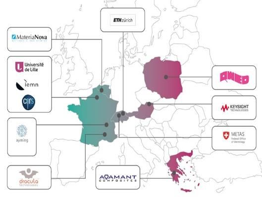
MMAMA project (Microwave Microscopy for Advanced and
Efficient Materials Analysis and Production) which will offer
a nanoscale characterization platform for the European
manufacturers of coatings, photovoltaic cells, and semi-
conductor circuits. Partners of the project will use a
combination of scanning microwave microscopes,
dielectric resonators, and simulation to measure the
material and interface properties of complicated material
systems and nano-structures. This project, launched on
November 1, 2017, will last 3 years. It received a European
funding of € 3.99 million, allocated by the Horizon 2020
research and innovation programme.
Workshop Chairs:
Dr. Johannes Hoffmann, METAS (Switzerland), Johannes.Hoffmann@metas.ch
Dr. Malgorzata Celuch, QWED (Poland), M.Celuch@qwed.eu
Workshop Title:
Material and Impedance Measurement Techniques
by MMAMA Project Partners and Stakeholders
Workshop Abstract:
MMAMA Workshop presents recent developments in material and impedance measurement
techniques. Following the introductory presentation of the MMAMA project, there are six talks from the
MMAMA consortium enriched with two from collaborating research groups at the Warsaw University of
Technology (WUT).
The first part of the Workshop is dedicated to nanoscale material characterterisation techniques, namely,
Scanning Microwave Microscopy from METAS and hybrid techniques from the University of Lille,
operating up to 110 GHz. A talk from the WUT Antenna and sub-THz Group presents quasi-optical
methods extending into sub-THz frequency range. The first part terminates with a modelling talk from
ETH Zurich, providing insight into the physics of nanoscale measurements.
The second part of the Workshop continues with modelling-based resonant methods of material
characterisation, including dielectric resonators from QWED and Fabry-Perot Open Resonator from
WUT. A Keysight talk shows how different form-factor VNAs are used and calibrated in conjunction with
resonators, coaxial probes, and antennas. A summarising user's perspective is provided by the talk from
MateriaNova.
To access the detailed agenda of the workshop.
Registration: https://mrweek.org/participant-registration/
Acknowledgements: This project has received funding from the European Union’s
Horizon 2020 research and innovation programme under grant agreement
MMAMA n° 761036.INTRODUCTION
EU H2020 Project MMAMA - Microwave Microscopy for Advanced and Efficient
Materials Analysis and Production
Speaker:
Kamel Haddadi
Kamel.Haddadi@univ-lille.fr
TALK 1
Nearfield Scanning Microwave Microscopes and Applications
Speaker:
Johannes Hoffmann
Johannes.Hoffmann@metas.ch
TALK 2
Nanoscale Hybrid Metrology Techniques and Data Fusion
Speaker:
Kamel Haddadi
Kamel.Haddadi@univ-lille.fr
TALK 3
Measurement systems for lossless and lossy materials up to sub-THz
frequencies
Speaker:
Yevhen Yashchyshyn
e.jaszczyszyn@ire.pw.edu.pl
TALK 4
Physical Modeling and Simulation of Microwave Microscopy of Semiconductor
Materials at High Frequencies
Speaker:
Arif Gungor
arifg@ethz.ch
TALK 5
Enhancements to dielectric resonator material measurement techniques
based on electromagnetic modelling and signal processing
Speaker:
Malgorzata Celuch
mceluch@qwed.eu
TALK 6
Measurement of Dielectrics from 20 to 110 GHz with a Fabry-Perot Open
Resonator
Speaker:
Bartlomiej Salski
b.salski@ire.pw.edu.pl
TALK 7
Fast and calibrated RF measurements for open-ended coaxial probes, 2D
dielectric imaging systems, and microwave imaging systems.
Speaker:
Mykolas Ragulskis
mykolas.ragulskis@keysight.com
TALK 8
Broad range spectral characterization methods from Hz to GHz: New
experimental set-up for measuring electrical properties in organic electronics
Speaker:
Olivier Douhéret
olivier.douheret@MATERIANOVA.BEINTRODUCTION
EU H2020 Project MMAMA - Microwave Microscopy for Advanced and Efficient
Materials Analysis and Production
Speaker:
Kamel Haddadi
Kamel.Haddadi@univ-lille.fr
Affiliation:
Univ. Lille, CNRS, Centrale Lille, Yncréa ISEN, Univ. Polytechnique Hauts-de-France, UMR
8520 - IEMN, F-59000 Lille, France
Abstract:
Industry offers a large range of organic and inorganic nanoparticles addressing numerous
manufacturing sectors and applications. The quality and performance of the final manufactured products
depend strongly on their chemical/electrical/optical/mechanical properties at nanoscale as well as their
arrangements at macroscale (amorphous, partially isomorph, hybrid/composite, multilayered). A similar
problem exists for thin-films. The constituting chemical elements of a thin film stack are usually known,
but the morphology, thickness of the layers and crystallization are decisive for the performance of the
final product. Macroscale measurements are needed to verify that these properties are correctly set on
the entire surface of e.g. a thin-film solar cell. For the domain of testing and characterization of materials
properties, there is also a very large gap between nano- and macro- worlds concerning the type of
instruments and methodologies as well as the type of measured data.
MMAMA, an H2020 European project, aims at solving this problem by offering a multiscale
characterization platform for the manufacturers of coatings, photovoltaic cells, and semi-conductor
circuits. It is proposed to use a combination of scanning microwave microscopy, free-space, coaxial and
dielectric resonator methods, and simulation to measure the material and interface properties of
complicated material systems and nano-structures.
The talk will give an overview of MMAMA by presenting partners involved, general objectives, results
achieved and on-going activities.
This project has received funding from the European Union’s Horizon 2020 research and innovation
programme under grant agreement No 761036.
TALK 1
Nearfield Scanning Microwave Microscopes and Applications
Speaker:
Johannes Hoffmann
Johannes.Hoffmann@metas.ch
Affiliation:
METAS, Switzerland
Abstract:
Nearfield scanning microwave microscopes are instruments to measure strongly localized material
parameters at microwave frequencies and lumped elements of microscopic size. Applications range
from semiconductors over fuel cell membrane inspection to biology. The technique consists in sending
an electromagnetic wave to a sharp metallic tip, which is in contact with a sample. At the tip, the
electromagnetic wave interacts with the sample and is reflected back to a receiving instrument. Material
parameters can be deuced from reflection amplitude and phase. The two most important components
of a nearfield scanning microscope are its tip because it directly determines the spatial resolution
(typically 10 nm to 100nm) and the used calibration technique and standards because they decide on
how the results can be used. The use of unshielded Pt/Ir tips is shown and a nearfield scanning
microwave setup for such tips is presented. Additionally, coaxial tips based on glass capillaries and the
required setups to use such tips are discussed. Different techniques for calibrating the nearfield
scanning microwave microscope and the respective calibration standards are compared. Additionally a
set of coplanar standards made of gold on a silicon nitride membrane are shown. Fabrication,measurement and simulation of these standards is discussed. Finally operating techniques of nearfield
microwave microscopes are discussed.
TALK 2
Nanoscale Hybrid Metrology Techniques and Data Fusion
Speaker:
Kamel Haddadi
Kamel.Haddadi@univ-lille.fr
Affiliation:
Univ. Lille, CNRS, Centrale Lille, Yncréa ISEN, Univ. Polytechnique Hauts-de-France, UMR
8520 - IEMN, F-59000 Lille, France
Abstract:
The traceability and accuracy of nano-measurement equipments such as atomic force microscopy
(AFM), scanning electron microscopy (SEM) or scanning microwave microscopy (SMM) ensure reliable
nanomanufacturing. An Advanced nano-metrology platform combining AFM, SEM and SMM into a
single instrument is developed for hybrid metrology and data fusion.
A new near-field scanning RF probe operating in the frequency range 1-110 GHz has been designed
and fabricated for providing simultaneously the topography and the RF complex impedance at the tip
apex of the probe with sub-20nm spatial resolution. The AFM mode is achieved by considering the
general deflection laser approach whereas the RF mode is achieved by feeding the probe by an RF
coaxial cable itself connected to vector network analyser. The system integrated into a SEM Tescan®
MIRA XMU has been designed to be as compact as possible. In contrast with conventional scanning
probe microscopes operating in air, mechanical manual adjustments of the laser deflection system are
not possible in the SEM. Consequently, laser beam and detector are mounted on nano-robotic piezo-
driven stages.
The unique capability of the instrument to provide hybrid data will be exemplary demonstrated by
considering measurements performed on topographic and electric reference samples. In particular, the
solution proposed provides a real time visualization of both the probe and the sample under
investigation.
References:
[1] K. Haddadi, O. C. Haenssler, C. Boyaval, D.Theron, and G. Dambrine. "Near-field scanning
millimeter-wave microscope combined with a scanning electron microscope." In 2017 IEEE MTT-S
International Microwave Symposium (IMS), pp. 1656-1659. IEEE, 2017.
[2] K. Haddadi, P. Polovodov, D. Théron, and G. Dambrine. "Quantitative Error Analysis in Near-Field
Scanning Microwave Microscopy." In 2018 International Conference on Manipulation, Automation and
Robotics at Small Scales (MARSS), pp. 1-6. IEEE, 2018.
[3] P. Polovodov, C. Brillard, O. C. Haenssler, C. Boyaval, D. Deresmes, S. Eliet, F. Wang et al.
"Electromagnetic Modeling in Near-Field Scanning Microwave Microscopy Highlighting Limitations in
Spatial and Electrical Resolutions." In 2018 IEEE MTT-S International Conference on Numerical
Electromagnetic and Multiphysics Modeling and Optimization (NEMO), pp. 1-4. IEEE, 2018.
TALK 3
Measurement systems for lossless and lossy materials up to sub-THz
frequencies
Speaker:
Yevhen Yashchyshyn
e.jaszczyszyn@ire.pw.edu.pl
Affiliation:
Institute of Radioelectronics and Multimedia Technology
Warsaw University of Technology
Contributors:
Konrad Godziszewski
Abstract:Fourier-transform infrared (FTIR) and Time-Domain (TDS) spectroscopies are widely used for material
characterization of materials in terahertz range. The main disadvantage of them is limited measurement
dynamics especially in lower frequency band. They also require using very thin samples in case of lossy
materials. New generation of vector network analyzers (VNA), which are very well known in microwave
band, allow measurements in frequency domain up to 1.5 THz with very high dynamics above 90 dB.
Moreover, the amplitude and the phase of signals can be measured at many frequency points with 1 Hz
resolution. These advantages create new opportunities in frequency domain characterization of different
types of materials, both lossless and lossy.
The activity of the Antenna and sub-THz Research Group of the Institute of Radioelectronics and
Multimedia Technology at Warsaw University of Technology in the field of characterization of dielectric
materials up to sub-terahertz frequencies will be presented. Additionally, two new advanced techniques
for lossless and lossy materials characterization will be described.
The first proposed technique for lossless dielectrics is based on a quasi-optical principle and an
interference technique. The peculiarity of this technique is the absence of a reference interference
channel and there is no need to rotate the sample under test. It simplifies the measurement process and
increases its accuracy. The reference channel is obtained by using two tiers measurement procedure
and VNA feasibility. The method provides accurate results in discrete frequencies, however many
measurement points in broad band are required to obtain at least one interference minimum.
The second method is dedicated for broadband characterization of dielectrics. Quasi-optical free space
measurement setup is used to determine the complex reflection coefficient in a wide frequency band.
This method makes it possible to characterize very dielectric by using only reflection without accurate
information about the thickness of dielectric sample. This method is useful in case of lossy and/or thick
dielectric samples and is based on modern measurement equipment feasibility, with the possibility to
make measurements in high number of frequency points. The mathematical model of the method is also
formulated.
TALK 4
Physical Modeling and Simulation of Microwave Microscopy of Semiconductor
Materials at High Frequencies
Speaker:
Arif Gungor
arifg@ethz.ch
Affiliation:
Institute of Electromagnetic Fields(IEF), ETH Zurich
Contributors:
Till Ehrengruber, Jasmin Smajic, Juerg Leuthold
Abstract:
Scanning Microwave Microscopy (SMM) is one of the high frequency methods to characterize and
provide information about materials and have been traditionally used for metals and dielectrics to
extract their permittivity and conductivity [1]. In order to bridge the gap between experiments and
parameters, and also to understand behavior of different types of materials, modeling and simulations
of such setups [2] have been done extensively. The models, however, mostly were only tackling the
electromagnetics, and for this purpose quasi-static or full wave electromagnetic solvers have been
employed. This work; nevertheless, will focus on coupled models which also incorporate
semiconductor physics.
The widely known semiconductor analysis is based on Poisson-Drift-Diffusion (PDD) equations and a
full-wave coupled solver together with PDD solver can already broaden understanding of SMM for
semiconductor materials for commonly used SMM frequencies [3]. This multiphysics solver enables to
observe transient charge dynamics and changing local effects in semiconductors with the applied
external electric field thanks to the coupled model. However at higher frequencies, PDD model
becomes inadequate for semiconductors, due to its classical assumptions such as constant mobility of
electric charge carriers. Thus, for such high frequencies, more advanced transport models, such as
Boltzmann Transport Equation (BTE), will be required to capture the carrier transport accurately. This
more general transport equation leads to Hydrodynamic Model (HDM) for semiconductors [4] which
can take inertia effects and velocity overshoot for carriers into account and therefore can model highfrequency transport with better accuracy. In this work, comparison of PDD and HDM will be presented
and multiphysics solvers (PDD-Maxwell and HDM-Maxwell) will be demonstrated for SMM of
semiconductors.
References:
[1] Hoffmann, J., G. Gramse, J. Niegemann, M. Zeier, and F. Kienberger, “Measuring low loss
dielectric substrates with scanning probe microscopes,” Appl. Phys. Lett. 105, 013102 (2014).
[2] Gungor, A.C., M. Celuch, J. Smajic, M. Olszewska-Placha, J. Leuthold, "Flexible Electromagnetic
Modeling of SMM Setups with FE and FDTD Methods," presented at 2019 IEEE MTT-S
International Conference on Numerical Electromagnetic and Multiphysics Modeling and
Optimization (NEMO), Boston, MA, USA, May 29-31, 2019.
[3] Gungor, A., J. Smajic, F. Moro, and J. Leuthold, “Time-domain Coupled Full Maxwell- and Drift-
diffusion-solver for Simulating Scanning Microwave Microscopy of Semiconductors," Submitted
and accepted to PIERS, 2019
[4] Ehrengruber, T., A. Gungor, K. Jentner, J. Smajic, and J. Leuthold, “Frequency Limit of the Drift-
Diffusion-Model for Semiconductor Simulations and its Transition to the Boltzmann Model,"
Submitted to CEFC, 2020
[5] H2020 MMAMA project reports. [Online]. Available: www.mmama.eu
TALK 5
Enhancements to dielectric resonator material measurement techniques
based on electromagnetic modelling and signal processing
Speaker:
Malgorzata Celuch
mceluch@qwed.eu
Affiliation:
QWED Sp. z o.o., Warsaw, Poland
Contributors:
QWED: Wojciech Gwarek, Marzena Olszewska-Placha, Janusz Rudnicki, Olga Stec
WUT: Jerzy Krupka
Abstract:
Dielectric resonator test-fixtures [1] are well established for material characterisation at microwave
frequencies. In particular, the split-post dielectric resonator (SPDR) method has become an international
standard [2], renown for its ease-of-use and high accuracy, especially in the case of low-loss dielectrics.
Our activities in the MMAMA project are concerned with obviating the limitations of the SPDR technology
with regard to dimensions of measurable samples and lateral resolution of the measurement.
In the first part of this talk, we discuss the application of electromagnetic (EM) modelling tools of
QuickWave series to commercially available SPDRs. The simulation results allow us to illustrate the
physics of SPDR measurements and provide the basis for downscaling material images below the size
of the SPDR head.
In the second part, we demonstrate a 2D surface scanner incorporating a 10 GHz SPDR. When working
in an automatic regime, it imposes stringent requirements on the speed and accuracy of extracting
resonant frequencies and Q-factors from the transmission characteristics of the resonator. Several
algorithms based on noise filtering and curve matching are discussed and optimum settings for scalar
and vector network analysers used in the setup are proposed. The setup is controlled by a laptop
application (MUCA).
In the third part, the above two groups of project deliverables are combined into a new technique of
automatic imaging of dielectric material surfaces at sub-head resolution. Samples of dimensions up to
100 mm x 100 mm are automatically scanned, with a typical scanning step of 1 mm. Raw images (of
head-size resolution) are downscaled using three different methodologies, namely, in the Fourier- [3],
space- [4], and wavelet - domain. The hardware and software presented in this talk will be available for
hands-on experience during the Workshop and throughout MIKON Conference in QWED exhibition
booth.References:
[1] J. Krupka, A. P. Gregory, O. C. Rochard, R. N. Clarke, B. Riddle, and J. Baker-Jarvis, “Uncertainty
of complex permittivity measurements by split-post dielectric resonator technique”, J. Eur. Ceramic Soc.,
vol. 21, pp. 2673-2676, 2001.
[2] European Standard: IEC 61189-2-721:2015.
[3] P. Korpas, “Deconvolution-based spatial resolution improvement technique for resistivity scans
acquired with split-post dielectric resonator”, Proc. 22nd Intl. Microwave and Radar Conf. MIKON,
pp. 541-543, Poznan, PL, May 2018.
[4] M. Celuch, W. Gwarek, A. Wieckowski, "Enhanced-resolution material imaging with dielectric
resonators: a new implicit space - domain technique", IEEE MTT-S Intl. Microwave Symp. 2019, Boston,
June 2019, pp. 55-58.
TALK 6
Measurement of Dielectrics from 20 to 110 GHz with a Fabry-Perot Open
Resonator
Speaker:
Bartlomiej Salski
b.salski@ire.pw.edu.pl
Affiliation:
Institute of Radioelectronics and Multimedia Technology
Warsaw University of Technology
Contributors:
Tomasz Karpisz, Pawel Kopyt, Jerzy Krupka
Abstract:
A novel approach to the measurement of complex permittivity of low-loss dielectric materials with the
aid of a Fabry-Perot open resonator with concave Gaussian mirrors will be presented. An automated
setup operating in the 20-110 GHz range is applicable to detect changes of resonance frequencies and
of the corresponding Q-factors of consecutive Gaussian TEM0,0,q modes due to sample insertion. The
obtained results are, subsequently, compared with data computed with the aid of an electromagnetic
model of the resonator to extract the unknown complex permittivity of the material under test. For that
purpose, a new scalar one-dimensional layered model of the Fabry-Perot open resonator has been
proposed. The model takes the advantage of Cartesian to Gaussian coordinate transformation and
axisymmetrical properties of the modes of interest. The model more accurately accounts for oblique
incidence of the wave onto the surface of the sample, which is one of major challenges in case of
alternative models based on a characteristic equation. A real part of permittivity of a few well-known
materials, such as PET foil or PTFE, has been measured with the accuracy better than 0.5%,
which means a significant improvement as compared to the state-of-the-art in this area.
TALK 7
Fast and calibrated RF measurements for open-ended coaxial probes, 2D
dielectric imaging systems, and microwave imaging systems.
Speaker:
Mykolas Ragulskis
mykolas.ragulskis@keysight.com
Affiliation:
Keysight Labs Austria
Contributors:
Keysight: Manuel Kasper, Ivan Alic, Amin Moradpour, Ferry Kienberger
QWED: Malgorzata Celuch, Janusz Rudnicki
National University of Ireland: Niko Istuk, Emily Porter, Martin O’Halloran
Abstract:
Accurate knowledge of material dielectric properties is fundamental for numerous applications including
materials science, in-line materials characterization and quality control, as well as microwave imaging
systems where multiple antennas are used. In the first part of this presentation we show fastmeasurements of dielectric properties with a small size microwave transceiver done together in a
collaboration with National University of Ireland. By replacing the traditional swept frequency VNA from
the dielectric measurement system with a more compact microwave transceiver we achieve faster and
more accurate measurements. The microwave transceiver uses novel broadband, multi-tone source
and broadband receivers to capture the instantaneous S-parameters at multiple tones simultaneously.
We conducted dielectric properties measurements on standard liquids which have known dielectric
properties using our modified setup and compared the results with the theoretical values. We also
conducted the same measurements with the typical setup which includes the swept frequency VNA and
compared the performances of the two measurement setups. We concluded that the microwave
transceiver can provide faster measurement speeds than the conventional VNA without sacrificing
measurement precision and accuracy. In the second part we show a prototype of microwave-portable
dielectric-probe and dielectric-resonator kits for micro- and millimeter scale permittivity evaluation on
large samples. Here we show the integration of an existing 10 GHz SPDR from QWED into a two-
dimensional lateral scanning system developed by QWED, with the resonator interfaced to a 2-port VNA
from Keysight, that precisely measures the resonant frequency and the quality factor (Q-factor) for each
spatial pixel. Electromagnetic modelling and calibration allow to map the measured resonant properties
into complex permittivity resulting in a 2D image of the real- and imaginary part, as developed by QWED.
An example is shown on samples from Materia Nova, Belgium. The small form factor of the Keysight
FieldFox together with the self-contained scanner allows for compact system design enabling the
integration into industrial in-line production environments as shown for solar cell materials. In the third
part, we present a fast S-parameter calibration procedure for microwave imaging systems where
multitude of antennas are used. By using the electronic calibration module (ECal), one port of the system
is calibrated and the calibration plane is moved to the antenna connector. Assuming that all antennas
interact with the calibration dielectric material in the same way, the one-port calibration is transferred to
all antennas. For full calibration including reflection and transmission parameters, the ‘unknown thru’
technique is used. This calibration procedure is valid for any number of antennas and it can be fully
automated for in-line applications.
TALK 8
Broad range spectral characterization methods from Hz to GHz: New
experimental set-up for measuring electrical properties in organic electronics
Speaker:
Olivier Douhéret
olivier.douheret@MATERIANOVA.BE
Affiliation:
Materia Nova R&D Center, Belgium
Contributors:
Materia Nova: David Moerman
Keysight: Georg Gramse, Ferry Kienberger
Univ. Lille: Didier Théron
Abstract:
Along with microelectronics standards in which device operating principles are based on monocrystalline
IV and III-V materials, semiconducting properties have more recently been observed in other materials
such as π-conjugated macromolecules and polymers and so-called organic semiconductors. Not only
their ability to transport carriers but also to absorb and/or emit light opened the doors to alternative
optoelectronic devices such as light-emitting or photovoltaic diodes and thin film transistors [1]. Low-
cost manufacturing processes and environmental footprint, large area devices, compatibility with flexible
layout count among the driving forces and the high expectations for this emerging technology.
While intensive academic research has been carried out since the turn of the century, key issues remain
to be overcome to be granted full industrial deployment from the existing and dedicated pioneer
companies. Among these issues, much remains to be understood in terms of charge transport in
complex structures in which both bulks and interfaces exhibit complex and peculiar properties depending
not only the materials themselves but also the fabrication processes. And if usual characteristics of
microelectronics standards can sometimes be also observed, the physical mechanisms that
underpinned these characteristics still need to be elucidated.
With a user’s perspective, this work demonstrates the ability and the complementarity of impedance and
microwave characterisation methods to efficiently probe carrier density and derive transport properties,hence the electrical properties in organic semiconductors. The case study is carried out on several donor and acceptor-like semiconducting polymers typically composing photovoltaic bulk heterojunction blends in organic solar cells [2,3]. Impedance spectroscopy measurements allow for simultaneous probing of conductance and capacitance of the material under test. The large broadband ranging between 10 Hz to 100 MHz leads to a spectral response from which the contribution from bulk, interfaces and external mechanisms in the overall transport mechanism can be identified and discriminated. Carrier mobility, interfacial barrier height and dielectric permittivity are among physical parameters derived from the measurements. Enhancing the broadband towards higher frequencies yet maintaining precisely calibrated instrumentation allow for further exploration and bridge the spectral gap towards microwave characterisation methods. The sensitivity of microwave characterization methods to variations of charge carrier density in semiconducting polymers was evidenced at the nanoscale with scanning microwave microscopy (SMM). The proposed experimental protocol is shown to detect capacitive and conductive mechanisms in the ac-biased polymer using a Mach-Zehnder interferometer-based detection system. Meanwhile, SMM allows for tunability of the frequency of the reflected microwave, leading towards in-depth three- dimensional probing of these semiconducting thin films. Through this user’s perspective approach, this study highlights the pertinence of the impedance and microwave methods for efficient and versatile electrical characterization of π-conjugated materials and blends, as promising probing tools for the incoming development of organic electronics. References: [1] Handbook of Organic Materials for Electronic and Photonic Devices edited by O. Ostroverkhova, Woodhead Publishing Series in Electronic and Optical Materials, UK, Elsevier 2019 [2] Cheng, P.; Wang, R.; Zhu, J.; Huang, W.; Chang, S.-Y.; Meng, L.; Sun, P.; Cheng, H.-W.; Qin, M.; Zhu, C.; Zhan, X.; Yang, Y., “Ternary System with Controlled Structure: A New Strategy toward Efficient Organic Photovoltaics”. Advanced Materials 2018, 30 (8), 1705243 [3] Moerman, D.; Sebaihi, N.; Kaviyil, S. E.; Leclère, P.; Lazzaroni, R.; Douhéret, O., „Towards a unified description of the charge transport mechanisms in conductive atomic force microscopy studies of semiconducting polymers”. Nanoscale 2014, 6 (18), 10596-10603.
You can also read