Helical Liquids in Semiconductors - Topical Review
←
→
Page content transcription
If your browser does not render page correctly, please read the page content below
Topical Review

                                                     Helical Liquids in Semiconductors
arXiv:2107.13553v1 [cond-mat.mes-hall] 28 Jul 2021

                                                                     Chen-Hsuan Hsu1 , Peter Stano1,2 , Jelena Klinovaja3 , and
                                                                     Daniel Loss1,3
                                                                     1 RIKEN    Center for Emergent Matter Science (CEMS), Wako, Saitama
                                                                     351-0198, Japan
                                                                     2 Institute of Physics, Slovak Academy of Sciences, 845 11 Bratislava, Slovakia
                                                                     3 Department of Physics, University of Basel, Klingelbergstrasse 82, CH-4056

                                                                     Basel, Switzerland

                                                                     30 July 2021

                                                                     Abstract. One-dimensional helical liquids can appear at boundaries of certain
                                                                     condensed matter systems. Two prime examples are the edge of a quantum
                                                                     spin Hall insulator, also known as a two-dimensional topological insulator, and
                                                                     the hinge of a three-dimensional second-order topological insulator. For these
                                                                     materials, the presence of a helical state at the boundary serves as a signature
                                                                     of their nontrivial bulk topology. Additionally, these boundary states are of
                                                                     interest themselves, as a novel class of strongly correlated low-dimensional systems
                                                                     with interesting potential applications. Here, we review existing results on
                                                                     such helical liquids in semiconductors. Our focus is on the theory, though
                                                                     we confront it with existing experiments. We discuss various aspects of the
                                                                     helical states, such as their realization, topological protection and stability, or
                                                                     possible experimental characterization. We lay emphasis on the hallmark of these
                                                                     states, being the prediction of a quantized electrical conductance. Since so far
                                                                     reaching a well-quantized conductance remained challenging experimentally, a
                                                                     large part of the review is a discussion of various backscattering mechanisms
                                                                     which have been invoked to explain this discrepancy. Finally, we include topics
                                                                     related to proximity-induced topological superconductivity in helical states, as an
                                                                     exciting application towards topological quantum computation with the resulting
                                                                     Majorana bound states.

                                                     Keywords: topological insulators and superconductors, helical channels, helical
                                                     Tomonaga-Luttinger liquids, charge transport, Majorana bound states

                                                     Submitted to: Semicond. Sci. Technol.
Helical Liquids in Semiconductors                                                                                                     2

1. Introduction                                                       (a)
                                                                               ↑           ⊕
In relativistic quantum field theory, spin-1/2 particles
are governed by the Dirac equation. The Dirac                                       Δz
Hamiltonian commutes with the helicity operator, the                           ↓           ⊖
projection of a particle spin on the direction of its
momentum. Therefore, helicity, defined as the sign of                        spin        helicity
the eigenvalue of the helicity operator, is an invariant                    splitting    splitting
of motion.‡ It allows one to assign a definite—negative
or positive—helicity to eigenstates, as illustrated in                Figure 2. (a) The degeneracy for spin-1/2 fermions can be
                                                                      lifted either by the Zeeman splitting ∆z or by helicity-dependent
Figure 1(a).
                                                                      interactions. When the Fermi energy crosses only one of the
                                                                      branches, the system is spin-polarized or has a definite helicity.
                                           (b)     spin               (b) Assuming that the chemical potential lies within an energy
                                                                      window where only states with a definite helicity are populated,
                                                                      the conduction modes are made of helical states whose spin
                                                            ↑&↓       orientation is fixed by the propagation direction.

                                       E         helicity
                                                                      degeneracy of the opposite spin states can be lifted, as
                                             k              ⊕&⊖       illustrated in Figure 2(a).
                                                                            Alternatively, one can image that, if the two
Figure 1. Notion of helicity. (a) In particle physics, the helicity   states with the opposite helicities can be split in
of a particle is defined through the relative orientation between     energy, one can create a helical liquid, with one of
its spin and momentum. (b) In a condensed matter system
hosting spin-1/2 fermions with quadratic dispersion, we can label
                                                                      the helicity states being occupied [see Figure 2(a)].
the degenerate states near the Fermi level either by their spins      In real space, such a system hosts conduction modes
or by their helicities. Unlike the spin, the states with opposite     made of helical states with spin orientation fixed by the
helicities can be split in a time-reversal-invariant system.          propagation direction; an example with the negative
                                                                      helicity is shown in Figure 2(b). Furthermore, in
      In a condensed matter system consisting of spin-                contrast to lifting the spin degeneracy, since the helicity
1/2 fermions, the low-energy Hamiltonian can mimic                    is invariant under time reversal, the helical liquid can
Dirac fermions and one can define the helicity of                     be generated in a time-reversal-invariant setting.
a fermionic state according to its momentum and                             While the fermion doubling theorem has proven
spin in a similar manner. Assuming that the Fermi                     that a helical liquid with an odd number of components
momentum is nonzero, one can label the states at                      (thus including a single pair of helical states) cannot
the Fermi level (which have intrinsic spin degeneracy)                be formed in a purely one-dimensional system (Wu
according to their helicity instead of spin.§ We                      et al. 2006), the theorem can be circumvented by
illustrate the two sets of labeling in Figure 1(b)                    having a helical liquid as a part of two- or three-
for particles with quadratic dispersion. The first                    dimensional systems.        Indeed, recent progress in
set of labeling can be straightforwardly examined in                  condensed matter physics has demonstrated that it is
experiments. Namely, upon applying a magnetic                         possible to stabilize such a helical liquid at boundaries
field, which has a Zeeman coupling to the spin, the                   of a higher-dimensional bulk.
‡ Strictly speaking, the helicity of a massive particle is not an           In this review, we focus on such gapless helical
intrinsic property, as the sign of momentum might change upon a       states flowing along the edges of two-dimensional
Lorentz boost, thus depending on the reference frame. However,        or hinges of three-dimensional bulk materials. The
being an invariant of motion, the helicity can serve as a good
quantum number in a given reference frame.
                                                                      helicity degeneracy is lifted due to the topology of
§ In analogy to particle physics, we define the helicity through      the bulk, which results in one-dimensional helical
the spin projection onto its quantization axis, even though the       channels appearing on the boundaries. The research
latter does not need to be in parallel to the momentum. In more       on helical channels has both fundamental and practical
general terms, states of the same helicity are defined such that
they form a time-reversal (Kramers) pair.                             motivations. First, as mentioned above, they appear
                                                                      on surfaces of certain materials in a way analogous to
Helical Liquids in Semiconductors                                                                                   3

the chiral edge states in the quantum Hall effect under      the foundations for the next sections.         We also
external magnetic fields. Since their existence is related   discuss how to detect and characterize the helical
to the bulk topology (Kane & Mele 2005b), their              channels.     In section 4, we discuss mechanisms
presence serves as a signature for the bulk topological      which can lead to backscatterings and therefore
phase (quantum spin Hall effect) that goes beyond the        affect the electrical conductance of a helical channel.
notion of Landau’s spontaneous symmetry breaking.            We divide the backscattering mechanisms into two
Second, being spatially confined in a narrow channel,        types–perturbations which break the time-reversal
the role of electron-electron interactions increases,        symmetry (section 4.2) and those which preserve it
offering a possible realization of a (quasi-)one-            (section 4.3). Since the resistance mechanisms are
dimensional strongly correlated fermion system (Wu           distinguishable through their temperature dependence,
et al. 2006, Xu & Moore 2006). As we will see,               we summarize the latter in Table 1 and Table 2 for
while interactions can potentially destabilize the helical   time-reversal symmetry breaking and time-reversal-
liquid, in other scenarios they can drive the helical        invariant mechanisms, respectively. In section 5, we
liquid into various phases ranging from magnetic orders      discuss how topological superconductivity arises upon
to topological superconductivity. In other words,            adding proximity-induced superconducting pairing,
combining the electron-electron interactions with other      and how Majorana bound states arise in various setups.
ingredients such as magnetic impurities, spin-orbit          We give an outlook in section 6.
coupling and superconducting pairing, helical states              We point out review articles on related topics,
provide a platform for unconventional states of matter.      both recent (Sato & Ando 2017, Haim & Oreg 2019,
     Apart from academic motivations, the helical            Gusev et al. 2019, Beenakker 2020, Culcer et al. 2020)
channels are also candidates for potential applica-          and less recent ones (Hasan & Kane 2010, Qi & Zhang
tions, for example in spintronics or topological quan-       2011, Maciejko et al. 2011, Alicea 2012, Beenakker
tum computation (Moore 2009). First, in contrast             2013, Das Sarma et al. 2015). Compared to those,
to ordinary one-dimensional channels, the topologi-          we focus on the charge transport properties of the
cal origin of helical channels protects them from An-        one-dimensional helical channels themselves. Also, we
derson localization due to weak disorder, possibly of-       cover more recent developments, such as the possibility
fering low-dissipation charge and spin transport at          of helical hinge states in higher-order topological
nanoscales (Sheng et al. 2005, Sheng et al. 2006). Sec-      insulators or realizations of Majorana bound states
ond, as their spin degeneracy is lifted, they can be used    using them.
to produce Majorana or parafermion modes for quan-
tum computation (Fu & Kane 2009, Mi et al. 2013, Kli-        2. Realization of helical edge states
novaja et al. 2014).
     As we discuss in depth below, many of these ex-         2.1. Quantum spin Hall effect
pectations turn out to be much more involved in re-
ality. Nevertheless, these prospects initiated extensive     We start with how the helical states are realized in
research on topological and strongly correlated systems      solid-state systems. As mentioned in section 1, even
over the past decade. Especially the investigations of       though a single pair of helical states cannot arise in
the quantized charge conductance, as the paramount           a purely one-dimensional system, it can appear on
property predicted for helical channels, continued un-       the one-dimensional edge of a two-dimensional system
abated in both theory and experiments. In particular,        hosting the quantum spin Hall state, a time-reversal-
the possible mechanisms for the unexpected deviation         invariant analog of the quantum Hall state (Kane
from the quantized conductance have been the subject         & Mele 2005a, Kane & Mele 2005b, Bernevig &
of numerous studies on helical channels. On the other        Zhang 2006, Wu et al. 2006, Xu & Moore 2006).
hand, the theoretical investigations, including those re-    This mechanism is closely related to the chiral edge
lying on the helical Tomonaga-Luttinger liquid (hTLL)        channels in a quantum Hall system. Here, the up-
model, are rather scattered in the literature. In addi-      and down-spin states feel effective magnetic fields with
tion to being not easy to track, they include several sets   opposite signs, leading to two copies of quantum Hall
of mutually contradicting results. This situation was        liquids with the opposite Hall conductance. Viewed
among our motivations to undertake a comprehensive           separately, each spin subsystem realizes a quantum
review on this topic.                                        Hall liquid hosting a chiral edge state with the opposite
     We organize the review as follows. In section 2,        chirality for the opposite spins. When combined, the
we discuss how the helical states arise on the               two spin subsystems host helical edge states, thus
boundaries of topologically nontrivial systems. In           preserving the time-reversal symmetry of the entire
section 3, we discuss the hTLL realized in the edge          system.
or hinge channels of the topological materials, setting           As an initial prediction, Kane and Mele proposed
                                                             that the quantum spin Hall effect can be realized in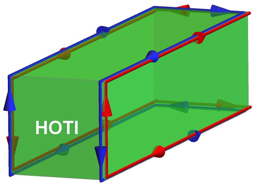
Helical Liquids in Semiconductors                                                                                         4

graphene (Kane & Mele 2005a), a state-of-art material       the identity matrix. Finally, the lower block is related
at that time (Novoselov et al. 2004, Castro Neto            to the upper one through the time-reversal symmetry.
et al. 2009). The key ingredient driving this effect        The basis for the above Hamiltonian comprises |E, +i,
is spin-orbit coupling: entering as an imaginary spin-      |H, +i, |E, −i, and |H, −i with E, H denoting the
dependent hopping term in a tight-binding model of          electron- and (heavy-)hole-like bands in HgTe/CdTe
graphene, it results in the spin-dependent magnetic         and ± denoting the time-reversal indexes. In addition
field required for the quantum spin Hall state. Similar     to the time-reversal symmetry imposed in (1), the form
to chiral edge channels of a quantum Hall liquid,           of hbhz (k) is further restricted by parity, the eigenvalue
which led to the notion of topological order, the           under the operation of spatial inversion. Using ↑ or ↓
helical edge channels of a quantum spin Hall state          to label the spin, and s or p the orbitals, the electron-
are protected by the energy gap of the bulk. The            like band |E, ±i consists of states |s, ↑ / ↓i while the
quantum spin Hall state in the Kane-Mele model was          hole-like band |H, ±i of | ± (px ± ipy ), ↑/↓i. Since these
subsequently identified as a Z2 topological order (Kane     two sets have opposite parity, the matrix elements h0
& Mele 2005b), a novel state distinct from an ordinary      and h3 must be even and the elements h1 and h2
insulator or a quantum Hall liquid with broken time-        must be odd under inversion. Taken together, the
reversal symmetry. The new classification relies on         time-reversal, inversion and crystal symmetries impose
a Z2 topological invariant constructed from the bulk        the following functional form for the matrix elements
Hamiltonian (Sheng et al. 2006, Moore & Balents             Taylor-expanded in momentum components around
2007).     In a bulk-boundary correspondence, the           k = 0 (Bernevig et al. 2006, König et al. 2007),
invariant is related to the number of the Kramers pairs
                                                            h0 (k) = Cbhz − Dbhz (kx2 + ky2 ),
of helical states on the boundary.
      Even though later it became clear that the spin-      h1 (k) = Abhz kx ,
                                                                                                                         (2)
orbit coupling, and the resulting gap, in graphene          h2 (k) = −Abhz ky ,
is too small to provide a quantum spin Hall phase           h3 (k) = Mbhz − Bbhz (kx2 + ky2 ),
under realistic conditions (Min et al. 2006, Yao et al.
2007), the work by Kane and Mele was seminal for            with the material- and structure-dependent parameters
subsequent investigations for more realistic setups. In     Abhz , Bbhz , Cbhz , Dbhz and Mbhz . The values of
the following we review the realizations of quantum         these parameters cannot be obtained from symmetry
spin Hall insulators, also known as two-dimensional         analysis.    Nevertheless, one sees that there is a
topological insulators (2DTI), in heterostructures          band inversion when the ratio Mbhz /Bbhz changes its
based on semiconductors.                                    sign. Crucially, this ratio is experimentally controllable
                                                            through the width of the HgTe layer, sandwiched
2.2. Quantum spin Hall effect in a semiconductor            by CdTe layers in the quantum well. As a remark,
quantum well                                                the bulk-inversion asymmetry in the zinc-blend lattice
                                                            induces an additional term not included in the BHZ
Among other theoretical proposals (Sheng et al.             model. However, detailed studies (Dai et al. 2008,
2005, Bernevig & Zhang 2006, Murakami 2006, Qi              König et al. 2008, Rothe et al. 2010) demonstrated
et al. 2006), a key contribution was made by                that while adding such a symmetry-breaking term
Bernevig et al., who predicted the quantum spin Hall        can affect the energy spectrum, it does not destroy
state in a composite quantum well made of HgTe              the topological phase transition that emerges in the
and CdTe (Bernevig et al. 2006). Owing to its               simplified model described by (1) and (2).
significance, here we review the BHZ model, named                For illustration, we solve numerically a tight-
after the authors of (Bernevig et al. 2006). It is          binding version of the BHZ model, using a two-
based on the k · p theory, a standard perturbation          dimensional rectangular grid with the lattice constant
theory for semiconductors, based on a restriction onto      a0 = 6.5 Å. The Hamiltonian HBHZ keeps the form
a few energy bands around the Fermi level. The BHZ          given in (1) with hµ for µ ∈ {0, 1, 2, 3} replaced
model is constructed from symmetry considerations for       by (König et al. 2008, Qi & Zhang 2011)
a quasi-two-dimensional quantum well grown along z                               Dbhz
direction with the in-plane momentum ~k = (~kx , ~ky )      h0 (k) = Cbhz − 2         [2 − cos(kx a0 ) − cos(ky a0 )],
                                                                                  a20
measured from the Γ point (k = 0). The BHZ model
Hamiltonian takes the following form,                                Abhz
                                                            h1 (k) =       sin(kx a0 ),
                                                                    a0
             hbhz (k)       0                                                                                    (3)
HBHZ =                              .              (1)                 Abhz
                0      h∗bhz (−k)                           h2 (k) = −       sin(ky a0 ),
                                                                        a0
Here, the upper block is hbhz (k) = h0 (k)τ0 + hµ (k)τµ ,                      Bbhz
with the Pauli matrices τµ for µ ∈ {1, 2, 3}, and τ0 is     h3 (k) = Mbhz − 2 2 [2 − cos(kx a0 ) − cos(ky a0 )].
                                                                                a0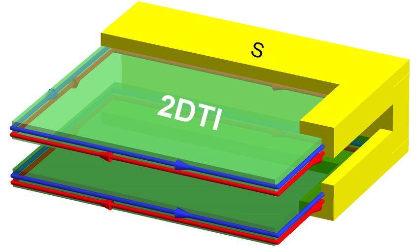
Helical Liquids in Semiconductors                                                                                                   5

                                                                   Figure 4. Spatial density profile, ρ(x), of the in-gap states in
                                                                   the band-inverted regime of the BHZ model. The states localized
                                                                   at the edge along x correspond to ones from Figure 3(b) for the
                                                                   energy within the bulk gap and for the propagation directions
    40                                                                                                                    > |2 for the
                                                                   along y as indicated in the insets. (a) Profile of |ψσ
          (b)                                                      eigenstates with positive velocity along y and spin σ. Here we
                                                                   set the chemical potential to 3.7 meV; the other parameters are
 E(ky )                                 Δb                     μ   the same as those adopted in Figure 3. (b) Similar to (a) but for
                                                                   negative velocity denoted as |ψσ< |2 . The gapless states with the
 [meV]
                                                                   opposite spins propagate in the opposite directions.

   -40
      -0.2      -0.1    ky a0     0.1        0.2 0 e2 /h   G       Along a specific edge, gapless states with opposite
                                                                   spins flow in the opposite directions; hence they are
Figure 3. Energy spectra of the BHZ model and the edge             helical. To distinguish the normal and the band-
conductance G as a function of the chemical potential µ. As        inverted regimes, a straightforward probe is through
indicated in the inset of Panel (a), we take zero boundary         the edge conductance. As illustrated in Figure 3, in
conditions along x and periodic along y. (a) Mbhz /Bbhz < 0.
                                                                   the normal regime, the conductance is zero when the
There is no state within the gap, leading to a trivial insulator
with zero conductance when µ lies in the gap. Here we adopt        chemical potential is in the gap. In contrast, when the
the parameter values: Abhz = 3.87 eV Å, Bbhz = −48.0 eV Å2 ,     band is inverted, we expect a finite—and in an idealized
Cbhz = 0, Dbhz = −30.6 eV Å2 and Mbhz = 0.009 eV,                 case, quantized—edge conductance when the chemical
corresponding to the quantum well width of 55 Å (Qi &
Zhang 2011). (b) Mbhz /Bbhz > 0. The bands are inverted,
                                                                   potential lies within the gap.
accompanied by gapless states propagating along the edges; see          Having demonstrated the presence of the helical
Figure 4. When the chemical potential lies within the bulk gap     edge states in the bulk gap, we now discuss how
∆b , the edge conductance is quantized. The adopted parameter      they are related to the bulk topology by examining
values are Abhz = 3.65 eV Å, Bbhz = −68.6 eV Å2 , Cbhz = 0,
Dbhz = −51.2 eV Å2 and Mbhz = −0.01 eV, corresponding to
                                                                   the Berry phase of the bulk eigenstates. Since the
the width of 70 Å (König et al. 2008, Qi & Zhang 2011).          upper and lower blocks in (1) are decoupled (which
                                                                   can be viewed as the up- and down-spin components),
                                                                   the Berry phase for the two blocks can be computed
These expressions reduce to (2) at small k. To calculate           separately. To this end, we define the Berry curvature
the energy spectrum, we consider a cylindrical                     as (Griffiths 1995)
geometry with zero boundary conditions along x and
periodic boundary conditions along y. To reflect                   Ωσ,± ≡ i5k × hΦσ,± (k)|5k |Φσ,± (k)i                           (4)
this geometry, we perform inverse Fourier transform                for the eigenstate |Φσ,± i with the periodic boundary
in the x coordinate and plot the eigenvalues as a                  conditions along both x and y directions. Here, for
function of ky , which remains a good quantum number.              each spin σ, the ± sign corresponds to the upper-
In Figure 3(a) where Mbhz /Bbhz < 0, the system                    /lower-band of the BHZ Hamiltonian with the (spin-
is fully gapped, indicating a trivial insulator with               degenerate) eigenvalues
zero conductance. In contrast, in Figure 3(b) with                         q
Mbhz /Bbhz > 0, the bands are inverted and gapless                 h0 (k) ± h21 (k) + h22 (k) + h23 (k),             (5)
states emerge within the bulk gap.           Looking at             where hµ are given in (3). As long as there exists a
the corresponding eigenfunctions plotted in Figure 4
                                                                    finite bulk gap, we can define the unit vector ĥσ ≡
reveals the following two properties of these gapless              ~hσ /|~hσ | with ~hσ = (σh1 , h2 , h3 ), and express the
states. First, they are localized at the edges. Second,
                                                                    nonzero (z) component of the Berry curvature as
they are spin polarized, and the spin polarization swaps
on inverting the velocity. In other words, these states                                1        ∂ ĥσ   ∂ ĥσ
                                                                   Ωσ,± ≡ Ωσ,± · ez = ∓ ĥσ · (       ×       ).                  (6)
are helical.                                                                           2        ∂kx     ∂ky
     A realistic sample is finite in both x and y
                                                                   The Berry phase is obtained upon integrating the
directions.     This case is illustrated in Figure 5.
                                                                   curvature over the momentum space. For convenience,
There are gapless edge states circulating around the
                                                                   we define the following quantity as the Berry phase
sample, whereas the interior of the system is gapped.
Helical Liquids in Semiconductors                                                                                                       6

                                                                      Figure 6. Parametric surface formed by the trajectory of the
Figure 5. Schematic of a two-dimensional topological insulator        unit vector ĥσ (blue arrow) when k = (kx , ky ) spans over the
(2DTI). While the interior (bulk states) of the system is gapped,     Brillouin zone. (a) In the trivial regime, the surface does not
there are gapless states located in the exterior, forming a helical   enclose the origin (red dot), making the winding number zero.
liquid circulating the edge.                                          (b) In the topological regime, the origin is enclosed by the surface
                                                                      once, leading to a winding number of unity (up to a spin-
                                                                      dependent sign). For the winding number to change through
divided by 2π,                                                        varying the Hamiltonian parameters, the surface has to pass
                                                                      through the origin, corresponding to the vector ~hσ vanishing
             d2 k
        Z
Nσ,± ≡            Ωσ,± ,                            (7)               at certain momentum and, thus, to a gap closing point.
          BZ 2π
with the integral over the Brillouin zone. It can
be shown that the above expression is the winding                     meet, the mass has to pass through zero, thus forming
number, which measures how many times the unit                        a domain wall, which can trap gapless states (Jackiw
vector ĥσ winds around the origin while (kx , ky )                   & Rebbi 1976). For a 2DTI, the band inversion leads
spanning the Brillouin zone (Hsu et al. 2011).                        to a bulk gap with negative mass and the vacuum
Therefore, it is quantized and cannot be continuously                 surrounding it corresponds to a trivial insulator with
varied unless the vector ~hσ shrinks to zero, which                   a positive mass.      Therefore, we have the bulk-
would require closing the bulk gap. Thus, the winding                 boundary correspondence–at the boundary separating
number is a topological invariant protected by the bulk               the topologically distinct regions, gapless edge states
gap, in analogy to Thouless-Kohmoto-Nightingale-den                   are stabilized.
Nijs (TKNN) invariant in the integer quantum Hall
states (Thouless et al. 1982).                                        2.3. Helical channels in various materials
     As illustrated in Figure 6, in the normal regime
                                                                      In addition to HgTe composite quantum wells, the
the trajectory of ĥσ does not enclose the origin and
                                                                      quantum spin Hall effect was predicted in InAs/GaSb
we have Nσ,± = 0, whereas in the inverted regime
                                                                      heterostructures (Liu, Hughes, Qi, Wang & Zhang
we get a nontrivial value Nσ,± = ∓σ. Assuming that
                                                                      2008). Here, it can be described by an extended
the chemical potential lies within the gap so that the
                                                                      BHZ model including additional terms induced by the
lower band is occupied and the upper band is empty,
                                                                      bulk inversion asymmetry and the surface inversion
we evaluate the total Chern number N and the spin
                                                                      asymmetry.       These additional terms modify the
Chern number Ns ,
     X                    X                                           location of the phase transition between the quantum
N≡       Nσ,− = 0, Ns ≡        σNσ,− = 2.           (8)               spin Hall and the trivial insulating phases (phase
       σ                        σ                                     boundary in the parameter space). However, they do
As a result, unlike the quantum Hall states labeled                   not alter the character of the phases that transit to each
by the total Chern number, here the bulk topology                     other, so the helical edge states are protected by the Z2
is characterized by the spin Chern number, which is                   invariant as in HgTe. In addition, the heterostructure
a Z2 invariant. Similar to the relation between the                   consisting of an electron layer and a hole layer allows
Chern number and the quantized Hall conductance                       inducing topological phase electrically, by a gate. Soon
(Thouless et al. 1982), here a nontrivial spin Chern                  after the theoretical proposals, quantum spin Hall
number indicates a quantized spin Hall conductance.                   states were reported in experiments in HgTe (König
     From the low-energy effective Hamiltonian of                     et al. 2007) and InAs/GaSb (Knez et al. 2011). For
a quantum spin Hall insulator, we can find a                          HgTe, a finite edge conductance is observed when the
correspondence between the topology of the system                     quantum-well width exceeds a critical value, whereas
and the sign of the mass of a Dirac fermion. Namely,                  a narrower well remains insulating. For both HgTe
the topological band-inverted regime is analogous to                  and InAs/GaSb, a conductance close to the quantized
a massive Dirac fermion with a negative mass while                    value was observed for sufficiently short edges. The
the trivial regime is characterized by a positive mass.               nonlocal conductance expected for edge transport was
At a boundary where two regions with opposite mass                    also demonstrated in (Roth et al. 2009) and (Suzuki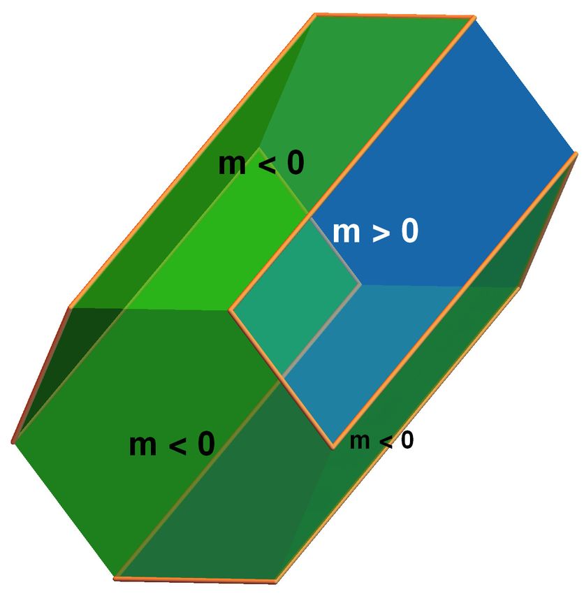
Helical Liquids in Semiconductors 7
et al. 2013) for these materials.
There are other quantum spin Hall systems poten-
tially hosting helical edge channels. Accompanied by
the rapid progress on novel van der Waals heterostruc-
tures (Geim & Grigorieva 2013), the quantum spin
Hall effect was predicted in two-dimensional transition-
metal dichalcogenides (Cazalilla et al. 2014, Qian
et al. 2014), including 1T’-WTe2 monolayer (Tang
et al. 2017), further boosting the community’s in-
terest in topological phases of monolayer materials.
The experimental indication of edge channels was re-
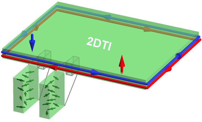
ported in 1T’-WTe2 monolayers (Tang et al. 2017, Wu Figure 7. Illustration of a three-dimensional second-order
topological insulator, where the bulk and surface are gapped.
et al. 2018). On the one hand, spectroscopic observa- (Left) The sign of the gap (Dirac mass) on a given surface,
tions of the gapless edge channels accompanied by a which depends on the surface orientation, is indicated by color.
bulk gap at the Fermi level through the scanning tun- (Right) At the hinges between two surfaces with opposite signs,
neling microscope (STM) and the scanning tunneling there are gapless helical states. The spin-up and -down hinge
states are separated for clarity. Here we illustrate a nanowire
spectroscopy (STS) were reported (Jia et al. 2017). On with a hexagonal cross section (realized in, for instance, Bi); for
the other hand, a contradicting STM study of (Song a square cross section, see Figure 15.
et al. 2018) concluded instead a semimetal-like gapless
bulk band structure. Furthermore, topological edge
channels were observed in spectroscopic measurements mass has to change its sign, and therefore go through
on bismuthene on SiC (Reis et al. 2017) and ultra- zero, at a hinge separating two neighboring surfaces of
thin Na3 Bi films (Collins et al. 2018), albeit these ma- opposite mass. In analogy to 2DTI, the sign change sig-
terials so far lack transport measurements. Remark- nifies closing the energy gap and appearance of gapless
ably, there was an experimental indication of a hTLL helical channels. In consequence, three-dimensional
along the edge channels of bismuthene on SiC (Stühler helical second-order topological insulators are charac-
et al. 2019). In comparison to earlier semiconductor- terized by one-dimensional gapless helical hinge states
based materials HgTe and InAs/GaSb, the more recent with opposite spin states propagating in opposite direc-
van der Waals heterostructures tend to have a larger tions, similar to spin-momentum locked edge channels
bulk gap and thus better topological protection for the in quantum spin Hall insulators.
edge states. Whereas currently there are only a handful Experimental indications for HOTI materials have
of examples of semiconductor-based materials hosting been reported in bismuth (Bi) nanodevices (Schindler,
helical channels, we expect the helical liquid to exist in Wang, Vergniory, Cook, Murani, Sengupta, Kasumov,
a broader variety of materials. Deblock, Jeon, Drozdov, Bouchiat, Guéron, Yaz-
Going beyond the two-dimensional nanostruc- dani, Bernevig & Neupert 2018, Murani et al. 2019),
tures, platforms hosting helical channels include van der Waals stacking of bismuth-halide (Bi4 Br4 )
higher-order topological insulators (HOTI). Relevant chain (Noguchi et al. 2021) and multilayer WTe2 in Td
to this review are three-dimensional helical second- structure (Choi et al. 2020, Wang et al. 2021). The the-
order topological insulators preserving time-reversal ory so far has not come to a consensus on the identity
symmetry (Langbehn et al. 2017, Song et al. 2017, of the bulk topology in Bi, claiming 2DTI (Murakami
Schindler, Cook, Vergniory, Wang, Parkin, Bernevig 2006, Wada et al. 2011), HOTI (Schindler, Wang,
& Neupert 2018, Khalaf 2018, Geier et al. 2018, Ezawa Vergniory, Cook, Murani, Sengupta, Kasumov, De-
2019, Călugăru et al. 2019, Plekhanov et al. 2020, Fang block, Jeon, Drozdov, Bouchiat, Guéron, Yazdani,
& Cano 2020, Tanaka et al. 2020), where both the Bernevig & Neupert 2018), topological crystalline in-
three-dimensional bulk and the two-dimensional sur- sulator with multiple nontrivial topological invari-
faces are gapped. One can generalize the above ants (Hsu, Zhou, Chang, Ma, Gedik, Bansil, Xu, Lin
notion of Dirac mass to this three-dimensional sys- & Fu 2019), or a system at the border between higher-
tem (Schindler 2020), in which the low-energy theory order and first-order (strong) topological insulating
can still be captured by the Dirac equation. Each of phases in a combined theoretical and experimental
the surfaces is described by the Dirac equation with study of (Nayak et al. 2019). In contrast to the di-
a finite Dirac mass. Distinct from a trivial insulator verse theoretical results, experimental studies are more
or a first-order topological insulator, the Dirac mass consistent, showing evidence in favor of edge or hinge
here depends on the surface orientation, as illustrated channels: An earlier STM study on locally exfoliated
in Figure 7. In this figure, the colors of the surfaces are Bi(111) bilayer showed topologically protected trans-
assigned according to the sign of the Dirac mass. The port over edges with length up to hundreds of nanome-
ters (Sabater et al. 2013). Additional support on the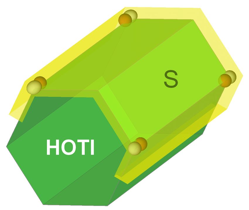
Helical Liquids in Semiconductors                                                                                                 8

existence of gapless hinge channels was seen in spec-
troscopic (Drozdov et al. 2014, Takayama et al. 2015)
and transport (Murani et al. 2017) experiments.

2.4. Other variations
Alternatively to these bulk topological materials, one
can produce a spin-selective gap in a (quasi-)one-
dimensional spin-degenerate semiconducting nanowire
combining Rashba spin-orbit interactions and mag-
netic field (Středa & Šeba 2003, Pershin et al. 2004,
Devillard et al. 2005, Zhang et al. 2006, Sánchez
et al. 2008, Birkholz & Meden 2009, Rainis & Loss
2014). The remaining gapless sector is then formed                 Figure 8.      Energy spectrum of a 2DTI, where k is the
by a pair of pseudo-helical states.k The difference                momentum along a given edge and µ is chemical potential. In
between the pseudo-helical and helical states in their             the energy window within the bulk gap ∆b near the Dirac point,
spectroscopy was pointed out by (Braunecker et al.                 one consider only the edge states and ignore the bulk states. For
                                                                   the illustrated spectrum, we have helical edge states composed
2012). Later, similar approach was adopted to carbon               of right-moving spin-down and left-moving spin-up states.
nanotubes, graphene nanoribbons, or 2DTI constric-
tions (Klinovaja et al. 2011, Klinovaja & Loss 2013,
Klinovaja & Loss 2015). We do not cover these pseudo-              case, it is well known that elementary excitations
helical states in systems where the time-reversal sym-             in interacting one-dimensional systems are of bosonic
metry is explicitly broken by the magnetic field. We               nature.    Such a system is known as Tomonaga-
refer the interested reader to recent reviews on this              Luttinger liquid (TLL), which differs strongly from a
topic (Prada et al. 2020, Frolov et al. 2020).                     Fermi liquid describing interacting fermions in higher
     Finally, it was proposed that hTLL can arise                  dimensions (Haldane 1981, Giamarchi 2003). Adding
in a cylindrical nanowire made of a (strong) three-                their helical nature, the edge or hinge states realize
dimensional topological insulator threaded by a                    a special form of matter, which is named helical
magnetic flux of a half-integer quantum (Egger et al.              Tomonaga-Luttinger liquid (hTLL) in this review.
2010). Alternatively, hTLL were proposed to occur                  Kane and Mele’s proposal on the quantum spin Hall
due a nonuniform chemical potential induced by gating              effect motivated investigations on such a helical liquid
across the cross-section of nanowire in the presence               formed along the edge of the system. It was shown
of the Zeeman field (Legg et al. 2021). However,                   that it embodies a novel class of matter (Wu et al.
since we are interested in helical states arising without          2006, Xu & Moore 2006), which is distinct from the
external magnetic fields, we do not cover this type of             spinful TLL (formed in spin-degenerate systems such
setups either. Besides, since we focus on solid-state              as semiconductor quantum wires) or the chiral TLL
systems, we do not cover realizations in other types of            (formed in the edge of a fractional quantum Hall
systems, such as photonic systems (Ozawa et al. 2019),             system). To discuss the properties of the hTLL, we
nonequilibirum/Floquet systems (Rudner & Lindner                   next introduce a description based on the bosonization
2020), magnonic systems (Nakata et al. 2017), or non-              formalism.
Hermitian systems such as cold atoms and topological                    Let us consider the hTLL located at an edge (a
circuits (Bergholtz et al. 2021).                                  hinge) of a 2DTI (HOTI). At energy scales within the
                                                                   bulk gap where the bulk states are absent,¶ the helical
3. Interacting helical channels: helical                           channel can be described as
Tomonaga-Luttinger liquid                                          Hhel = Hkin + Hee ,                                          (9)

After discussing how helical states arise at the edges             where Hkin and Hee are the kinetic energy and electron-
or the hinges of a topologically nontrivial system, we             electron interactions, respectively. In this section we
now turn to their own properties and how they can be               assume that the electron spin along the z axis S z
characterized. Since the helical states in either 2DTI             is a good quantum number. We will discuss the
edges or HOTI hinges are spatially confined in one-                generalization to a generic helical liquid, where S z
dimensional channels, one expects strong interaction               is not conserved, in section 4.3. Here, we further
and correlation effects. For the usual, nonhelical                 ¶ Beyond this energy scale, the hTLL description becomes
                                                                   invalid, as demonstrated in quantum Monte Carlo simulations
k In (Braunecker et al. 2012), these pseudo-helical states are     on the Kane-Mele model with Hubbard interaction (Hohenadler
termed “spiral” states as opposed to “helical” states in a 2DTI.   & Assaad 2012a, Hohenadler & Assaad 2012b).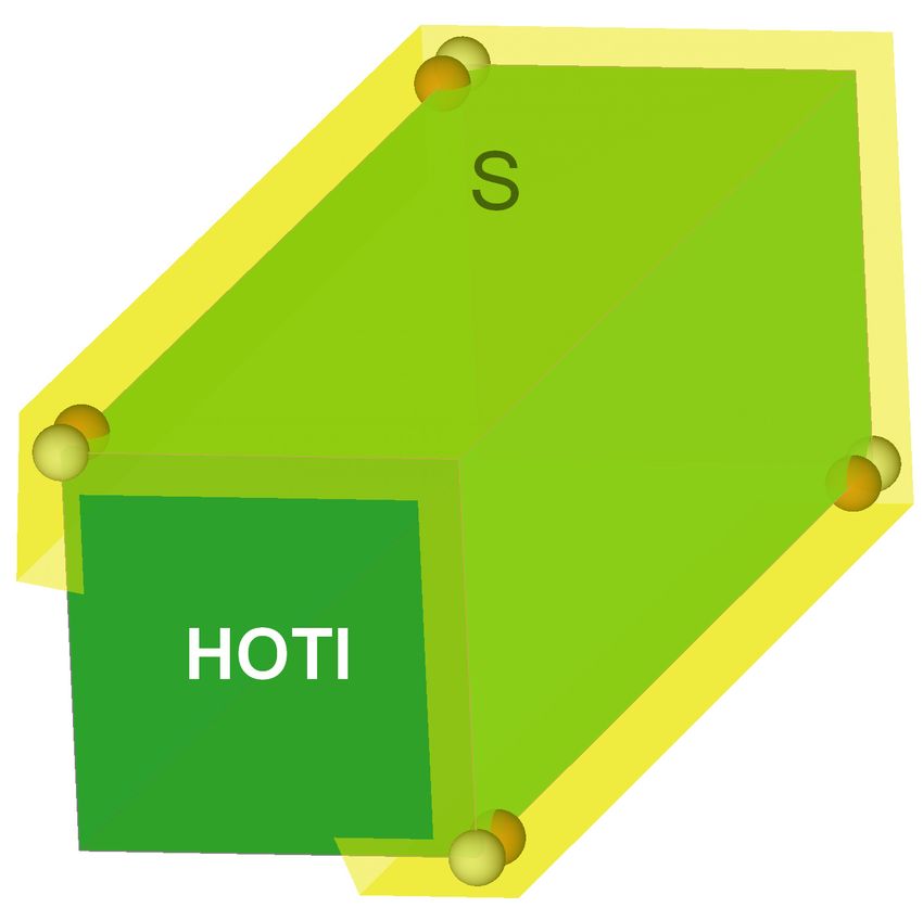
Helical Liquids in Semiconductors                                                                                 9

assume that the helical edge or hinge states are formed     InAs/(Ga,In)Sb devices (Li et al. 2017), K ≈ 0.4–
by right-moving spin-down and left-moving spin-up           0.6 for hinge channels in a bismuth HOTI (Hsu
electrons as in Figure 8. We can thus write                 et al. 2018b) and K ≈ 0.4–0.6 for bismuthene on
ψ↑ (r) = e−ikF r L↑ (r), ψ↓ (r) = eikF r R↓ (r),    (10)    SiC (Stühler et al. 2019).
                                                                  As we see in (15), the bosonized Hamiltonian is
with the slowly varying right(left)-moving fermion field    quadratic in the bosonic fields and can, therefore, be
R↓ (L↑ ), the coordinate r along the channel, and the       exactly diagonalized. In the bosonic language, one
Fermi wave vector kF of the helical states (measured        can thus perform calculations that are nonperturbative
from the Dirac point). From now on we will suppress         in the electron-electron interaction strength, including
the coordinate and the spin index unless it may cause       the renormalization-group (RG) analysis. Since the
confusion. The kinetic-energy term reads                    quantity K parametrizes the strength of Coulomb in-
                                                            teractions between electrons in the helical channel, it
                Z
Hkin = − i~vF dr R† ∂r R − L† ∂r L ,

                                                   (11)     serves as a crucial parameter for the RG relevance of
                                                            various interaction-induced and renormalized scatter-
with the Fermi velocity vF . The electron-electron
                                                            ing processes, as well as for the interaction-stabilized
interaction term is given by
          Z                                                 topological bound states, which we will discuss in the
Hee = g2 dr R† RL† L                                        following sections. It is, therefore, important to ex-
             Z                                              perimentally quantify this parameter in realistic set-
          g4       h       2      2 i                     tings. However, deducing the interaction parame-
       +        dr R† R + L† L          ,          (12)
           2                                                ter is tricky, especially from the—most common—dc
where g2 and g4 are the interaction strength describing     transport measurements. First, for a clean hTLL
the forward scattering processes.                           that is free from backscattering and adiabatically con-
     The fermion operators can be expressed in terms        nected to Fermi-liquid leads, it was found that the
of the bosonic fields (θ, φ),                               dc conductance of the helical channel does not de-
                                                            pend on K (Hsu et al. 2018a), resembling the bal-
           UR i[−φ(r)+θ(r)]
R(r) = √        e              ,                            listic conductance in a nonhelical channel (Maslov &
            2πa                                             Stone 1995, Ponomarenko 1995, Safi & Schulz 1995).
                                                     (13)
           UL i[φ(r)+θ(r)]                                  Second, while in the presence of backscattering sources
L(r) =   √      e            ,
            2πa                                             the conductance through a helical channel in general
where UR/L is the Klein factor and a = ~vF /∆b is           depends on the interaction strength, knowledge of the
the short-distance cutoff, which is associated with the     backscattering mechanism and resistance sources is re-
high-energy cutoff set by the bulk gap ∆b . The bosonic     quired to extract K. This complication makes the
fields satisfy                                              extraction of the experimental K value highly non-
                  π                                         trivial, as pointed out by (Väyrynen et al. 2016, Hsu
[φ(r), θ(r0 )] = i sign(r0 − r),                     (14)   et al. 2017, Hsu, Stano, Sato, Matsuo, Tarucha &
                   2
                                                            Loss 2019).
indicating that the field ∂r θ/π is canonically conjugate
                                                                  One may, therefore, consider alternative probes.
to φ. With (13), the helical channel Hamiltonian can
                                                            For instance, the ac conductivity σac (ω) of a hTLL
be bosonized as
              Z                                           can be measured optically without the influence of
         ~u           1        2         2                  the leads.       The real part of σac shows a zero-
Hhel =          dr      (∂r φ) + K (∂r θ) ,          (15)
         2π           K                                     frequency Drude peak with the weight depending on
where the velocity u and the interaction parameter K        the interaction strength (Hsu et al. 2018a, Meng,
are given by                                                Fritz, Schuricht & Loss 2014). Alternatively, one can
                             1                           search for spectroscopic signatures by probing the local
               g4 2  g2 2 2                              density of states, which exhibits a scaling behavior as
u ≡      vF +        −            ,             (16a)
              2π~       2π~                                 a function of energy E and temperature T (Stühler
                       1                                  et al. 2019),
        2π~vF + g4 − g2 2
K≡                         .                    (16b)
                                                                                    E

        2π~vF + g4 + g2                                     ρdos ∝ T  αdos
                                                                           cosh
                                                                                  2kB T
For repulsive electron-electron interactions (g2 , g4 >                                        2
0), we have K < 1.            For existing materials,                        1 + αdos      E
                                                                     × Γ              +i           ,            (17)
the interaction parameter was estimated in theory:                              2        2πkB T
K ≈ 0.2 for edge states in InAs/GaSb heterostruc-           with the Boltzmann constant kB and the interaction-
tures (Maciejko et al. 2009), K ≈ 0.53–0.9 for HgTe         dependent parameter αdos = (K + 1/K)/2 −
quantum wells (Hou et al. 2009, Ström & Johannesson        1.     Remarkably, this formula not only provides
2009, Teo & Kane 2009), K ≈ 0.43–0.5 for strained           spectroscopic signature for a hTLL, but also allows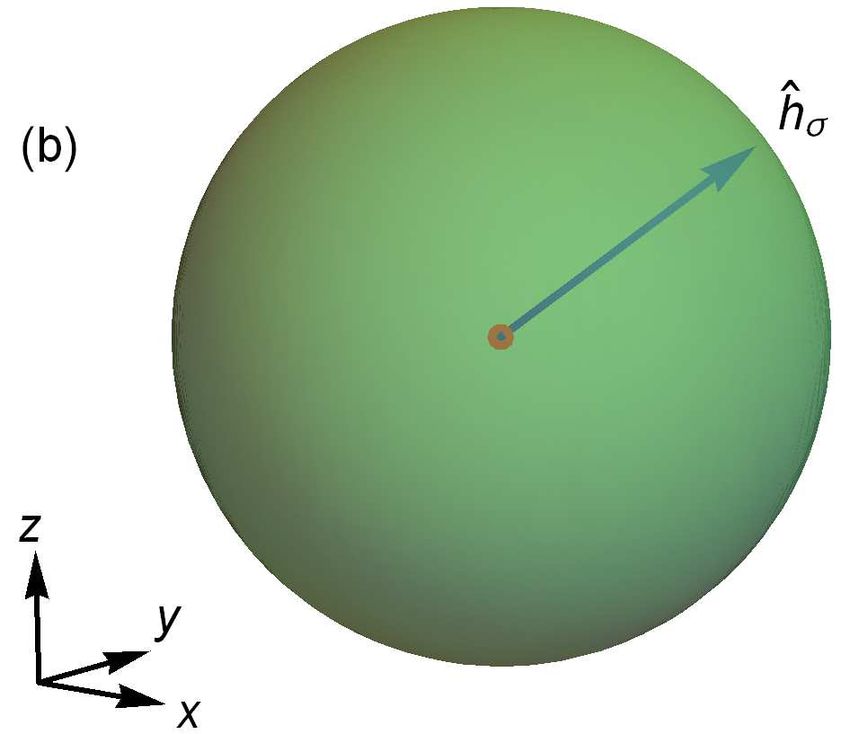
Helical Liquids in Semiconductors                                                                                10

for the extraction of the interaction parameter K.         4. Charge transport of a helical channel
This universal scaling behavior was indeed observed
on the edge of bismuthene on SiC through STS               The presence of one-dimensional helical channels can
measurements (Stühler et al. 2019), and the deduced       be experimentally examined through their charge
value of K was in good agreement with a theoretical        transport: A quantized conductance G0 = e2 /h
estimation. At T = 0, the expression reduces to            per channel is expected when the chemical potential
a power-law density of states depending on energy          lies within the bulk gap. In addition, the charge
ρdos ∝ |E|αdos as found earlier in the zero-temperature    transport has direct implications for applications in
calculation (Braunecker et al. 2012).                      electronics and spintronics. Below we first review the
     As an alternative, (Ilan et al. 2012) proposed a      experimental progress, before discussing the theoretical
setup to extract K by measuring the edge current           results on charge transport.
through an artificial quantum impurity, which is
realized by combining a local gate and an external         4.1. Experiments on edge transport
magnetic field. Since the artificial impurity acts as a
                                                           There are a number of transport measurements on
backscattering center with experimentally controllable
                                                           2DTI edge channels. For sufficiently short channels,
strength, one can determine K by fitting the edge
                                                           the expected ballistic value was observed in earlier
current to the analytical expression. Finally, (Müller
                                                           studies on HgTe (König et al. 2007), InAs/GaSb (Knez
et al. 2017) proposed a dynamical approach to
                                                           et al. 2011) and 1T’-WTe2 monolayers (Wu et al. 2018),
determine the interaction parameter of the 2DTI
                                                           along with observations consistent with nonlocal edge
edge states, from either time-resolved transport
                                                           transport in these materials (Roth et al. 2009, Suzuki
measurements with sub-nanosecond resolution or the
                                                           et al. 2013, Fei et al. 2017). Additional experimental
frequency dependence of the ac conductance.
                                                           features for helical channels include spin polarization
     While in principle the above proposals allow
                                                           of the edge states (Brüne et al. 2012) and real-space
one to extract the K value, using conventional—
                                                           imaging of edge current in HgTe (Nowack et al. 2013)
and thus well established—experimental probes seems
                                                           and InAs/GaSb (Spanton et al. 2014) based on mi-
more practical.        To this end, (Braunecker &
                                                           croscopic superconducting quantum interference device
Simon 2018) proposed the double-edge momentum
                                                           (SQUID). However, in contrast to the well quantized
conserving tunneling spectroscopy. It utilizes a setting
                                                           conductance of chiral edge channels in quantum Hall
analogous to the double-wire tunneling spectroscopy
                                                           states (von Klitzing et al. 1980, von Klitzing 2017), im-
based on cleaved edge overgrowth GaAs quantum
                                                           perfect quantization of the edge conductance was seen
wires (Auslaender et al. 2002, Tserkovnyak et al.
                                                           in longer samples. Moreover, the scanning gate mi-
2002, Tserkovnyak et al. 2003, Patlatiuk et al. 2018,
                                                           croscopy identified individual scattering centers (König
Patlatiuk et al. 2020), which has been used to detect
                                                           et al. 2013), which may originate from metallic puddles
the spinful TLL in semiconductor quantum wires.
                                                           formed in inhomogeneous potential landscape. These
Adopting it for helical channels, it requires a setup
                                                           observations triggered further studies on charge trans-
using a pair of controlled parameters: an applied bias
                                                           port of the potential 2DTI materials; such experiments
voltage between edges of two 2DTIs and a flux induced
                                                           were reviewed in (Gusev et al. 2019, Culcer et al. 2020).
by an external magnetic field penetrating in-between
                                                                 In most settings, the low-temperature conduc-
the edges. The bias voltage shifts the spectra of the
                                                           tance or resistance was weakly temperature depen-
two edges in energy, while the magnetic flux shits
                                                           dent, for both HgTe (König et al. 2007, Gusev et al.
them in momentum. A tunneling current then flows
                                                           2011, Grabecki et al. 2013, Gusev et al. 2014, Ol-
between the edges whenever the flux and bias meet the
                                                           shanetsky et al. 2015, Bendias et al. 2018) and
conditions for the energy and momentum conservation,
                                                           InAs/GaSb (Suzuki et al. 2013, Knez et al. 2014,
leading to an oscillating tunneling conductance as a
                                                           Suzuki et al. 2015, Du et al. 2015). In addition, a pe-
function of the magnetic field and the bias voltage. The
                                                           culiar fractional power-law conductance was observed
oscillation period allows one to deduce the parameter
                                                           in InAs/GaSb, which was attributed to hTLL sig-
K of a double-edge system with similar interaction
                                                           natures (Li et al. 2015). Furthermore, reproducible
strength. (Hsieh et al. 2020) extended the calculation
                                                           quasiperiodic fluctuations of both local and nonlo-
of (Braunecker & Simon 2018) to finite temperature
                                                           cal resistance as functions of gate voltage observed
and the presence of disorder, providing a systematic
                                                           in HgTe (Grabecki et al. 2013) became less pro-
analysis on the low-energy spectral function and the
                                                           nounced upon increasing the temperature, consistent
tunneling current.
                                                           with the expectations from charge puddles present in
                                                           narrow-gap semiconductors with inhomogeneous en-
                                                           ergy landscape. A more recent study on HgTe demon-
                                                           strated temperature-induced phase transition between
Helical Liquids in Semiconductors 11
the 2DTI and trivial insulating phases (Kadykov et al. quantum Hall state. On the other hand, the same
2018). For a 100-nm channel of WTe2 monolayer, the reference reports a large positive magnetoresistance
range for the temperature-insensitive conductance per- for |B|| | < 2 T, in contrast to the ballistic samples.
sists even up to 100 K (Wu et al. 2018), which is For |B|| | > 6 T, both local and nonlocal resistances
much higher than in the semiconductor heterostruc- quickly dropped with |B|| |. For |B|| | > 10 T, local
tures and is consistent with the theoretically predicted resistance saturated while the nonlocal one vanished,
large topological gap. suggesting the emergence of conductive bulk states
Concerning nonlocal transport, measurements on and thus a field-induced transition to a conventional
HgTe have been performed for samples of different bulk metal state. Similar results followed in their
sizes. On the one hand, the edge conductance is subsequent work (Gusev et al. 2013), which observed
well described by the Landauer-Büttiker formula for a decrease of the local resistance by B|| , accompanied
submicron-size samples in the ballistic regime (Roth by the complete suppression of nonlocal resistance by
et al. 2009). On the other hand, nonquantized B|| ≈ 10 T, consistent with a transition from 2DTI
resistance was observed for larger samples in the to a metallic bulk. A systematic investigation of the
diffusive regime (Grabecki et al. 2013) and for even field dependence of the edge transport was carried out
larger samples with channel lengths (perimeters of by (Ma et al. 2015), in combination with scanning
the samples) in the order of millimeter (Gusev et al. microwave impedance probe allowing for detection of
2011, Gusev et al. 2013, Olshanetsky et al. 2015). By the local electromagnetic response. Unexpectedly,
fabricating lateral p-n junctions in wide HgTe quantum whether B⊥ suppresses the edge conductance depends
wells with thickness of 14 nm, (Piatrusha et al. 2017) on the position of the chemical potential with respect
observed highly linear current-voltage characteristics, to the charge neutrality point. On the p-doped side, the
indicating transport via ballistic edge states. For edge conduction is gradually suppressed by applying
InAs/GaSb, (Suzuki et al. 2013) was able to observe B⊥ , whereas the edge conduction on the n-doped
dominant nonlocal edge transport in a micrometer- side shows little changes up to 9 T, contradicting the
long device by optimizing the InAs layer thickness, theoretical expectation. A recent study showed an
along with reproducible resistance fluctuations in the almost perfectly quantized edge conductance in a 6 µm-
gate voltage dependence, indicating multiple scatterers long edge at the zero magnetic field, which was strongly
along the channel. Utilizing a dual-gate device, suppressed by a small field of B⊥ = 50 mT (Piatrusha
(Suzuki et al. 2015) monitored the transition from the et al. 2019). With the field-induced broken time-
semimetallic to the 2DTI phase through the nonlocal reversal symmetry, they observed the exponential
resistance measurements. (Mueller et al. 2015) temperature dependence of conductance indicating
observed nonlocal edge transport with the resistance Anderson localization for the edge states, along with
systematically below the expected quantized values, reproducible mesoscopic resistance fluctuations as a
indicating a residual bulk conduction. For WTe2 , function of gate voltage and the gap opening in the
(Fei et al. 2017) demonstrated edge conductance in current-bias characteristics.
monolayer devices present over a wide range of gate Concerning different materials, surprisingly robust
voltage and temperature. On the other hand, the edge transport against magnetic fields was reported for
bilayer devices showed insulating behavior without a InAs/GaSb. Weak B|| dependence of edge conductance
sign of edge conduction. was observed (Du et al. 2015), which remained
To examine how the helical states respond approximately quantized up to 12 T. Nonetheless,
to broken time-reversal symmetry, one applies the magnetic fields can still modify the edge transport
external magnetic field. Measurements showed upon combining with electric fields. (Qu et al.
anisotropy with respect to the field orientation. For the 2015) demonstrated the tunability of the InAs/GaSb
ballistic regime of HgTe, (König et al. 2007) observed system through a dual-gate setting and magnetic fields.
a sharp cusp-like conductance peak centered at zero Utilizing the top and back voltage gates, which control
for an out-of-plane magnetic field B⊥ (perpendicular the Fermi level and the relative alignment between
to the two-dimensional heterostructure) and a much the electron and hole bands, together with B|| , which
weaker field dependence for an in-plane magnetic field shifts the two bands in momentum, they established
B|| . The observation was attributed to an anisotropic the phase diagram by measuring the local resistance.
Zeeman gap opening in the edge spectrum. (Gusev In contrast to the semiconductor heterostructures,
et al. 2011) examined a HgTe sample in the diffusive the edge conductance in WTe2 can be suppressed
regime under both B⊥ and B|| . They observed exponentially by either B|| (Fei et al. 2017) or B⊥ (Wu
an increasing resistance with a small B⊥ , which et al. 2018), demonstrating the Zeeman gap opening in
developed a peak and eventually was suppressed by the edge spectrum.
a strong field, probably due to a transition to a The peculiar features in HgTe and InAs/GaSbHelical Liquids in Semiconductors 12
under magnetic fields reported by (Ma et al. 2015, Du from the band-inverted to the band-normal regime,
et al. 2015) motivated theoretical works on “Dirac the conduction resembles the behavior of a disordered
point burial” or “hidden Dirac point” (Skolasinski et al. two-dimensional system. Therefore, even with the
2018, Li et al. 2018). Namely, detailed band structure most advanced fabrication, potential fluctuations are
calculations in these theoretical works revealed a Dirac sufficiently strong to destroy the topological state as a
point buried within the bulk valence or conduction result of the small hybridization gap.
bands. It results in a hidden Zeeman gap responsible Motivated by the fragile (and perhaps doubt-
for edge-state transport robust against magnetic fields. ful) topological nature of the InAs/GaSb heterostruc-
In addition to the unexpected temperature and ture, (Akiho et al. 2016) investigated strained
field dependencies, there exist other puzzles in experi- InAs/(Ga,In)Sb composite quantum wells, aiming at
ments, including a more recent observation of the local- engineering the band structure. The lattice mismatch
ization of HgTe edge channels with length of O(1 µm)– between the (Ga,In)Sb and AlSb layers in the het-
O(10 µm) in the absence of magnetic fields (Bubis erostructure induces a strain in the former layer, which
et al. 2021). Particularly for InAs/GaSb, the resid- enhances the hybridization between the electron band
ual bulk conduction in parallel to the edge transport of InAs and the hole band of (Ga,In)Sb. As a result,
was observed since its first 2DTI demonstration (Knez the bulk gap was increased by about two orders in com-
et al. 2011) and later on confirmed by scanning SQUID parison with the gap of InAs/GaSb. The edge trans-
microscopy (Nichele et al. 2016). It has motivated port of the strained material was subsequently con-
subsequent works on intentional impurity doping, ei- firmed by (Du et al. 2017), revealing weak tempera-
ther through Ga source materials with different im- ture dependence which can be fitted in a logarithmic
purity concentrations (Charpentier et al. 2013) or Si form (Li et al. 2017). Using the strained material, (Irie,
doping (Knez et al. 2014, Du et al. 2015). By sup- Akiho, Couëdo, Suzuki, Onomitsu & Muraki 2020)
pressing the bulk conduction with disorder, quantized demonstrated the gate-controlled topological phase
edge conductance with a deviation of about 1 % was transition along with the tunability of bulk energy gap,
observed in a wide temperature range (Du et al. 2015). which can reach above room temperature. (Irie, Akiho,
Alternatively, (Couëdo et al. 2016) employed specific Couëdo, Ohana, Suzuki, Onomitsu & Muraki 2020) in-
sample design, using a large-size device with asymmet- vestigated the effects of epitaxial strain on the topo-
ric current path lengths, to electrically isolate a single logical phase transition of InAs/GaSb by combining
edge channel and observed a conductance plateau close different substrate and buffer layers. Upon inducing
to the quantized value. biaxial tensile strain in the GaSb layer, they observed
There are also puzzles in the trivial regime of that the strain can close the indirect gap of the bulk
InAs/GaSb, where the energy bands are not inverted. spectrum, resulting a semimetallic behavior even in the
In contrast to the theoretical expectation, (Nichele band-inverted regime.
et al. 2016) observed edge channels even in the trivial While these great experimental efforts finally led
regime in the scanning SQUID microscopy. This to the observation of well quantized edge conduc-
observation was further confirmed in a device with the tance through gate training in macroscopic HgTe sam-
Corbino geometry, in which the conduction through ples with edge length in order of 100 µm (Lunczer
the bulk and edge states were decoupled (Nguyen et al. 2019), there are apparent discrepancies among
et al. 2016); these trivial edge states might share the the above experimental results, as well as between the
same origin as the counterpropagating edge transport observations and theoretical predictions. Motivated
observed in the quantum Hall regime of the InAs by these observations, numerous backscattering mech-
quantum well, as a result of the Fermi-level pinning anisms were proposed. In addition to being resistance
and carrier accumulation at the surface (Akiho et al. sources, since backscattering mechanisms might poten-
2019). The observation of (Nichele et al. 2016) tially localize the edge states and open a gap in the
motivated a systematic investigation (Mueller et al. edge or hinge energy spectrum, it is also important
2017) on length dependence of the edge resistances to examine the stability of the helical states against
in the nominally topological InAs/GaSb and trivial them. In the following subsections, we group the mech-
InAs materials. Importantly, the two systems showed anisms considered in the literature according to the
similar resistances with linear dependence on edge time-reversal symmetry. We discuss mechanisms that
length, clearly indicating the presence of multiple break the time-reversal symmetry in section 4.2, and
resistance sources. More recently, (Shojaei et al. those that preserve it in section 4.3.
2018) assessed the disorder effects due to charge In theoretical works, the charge transport is
impurities and interface roughness of a dual-gate device discussed in terms of various physical quantities,
by measuring the temperature and magnetic field including ac/dc conductivity, resistance, conductance
dependence of resistance. Upon tuning the system correction, or backscattering current. In order to makeYou can also read