In vacuum active colour sensor and wireless communication across a vacuum air interface - Nature
←
→
Page content transcription
If your browser does not render page correctly, please read the page content below
www.nature.com/scientificreports
OPEN In‑vacuum active colour sensor
and wireless communication
across a vacuum‑air interface
Osamu Sakai 1,2*, Takayuki Kitagawa3, Keiji Sakurai1, Go Itami1, Shigeyuki Miyagi1,2,
Kazuyuki Noborio3 & Kohshi Taguchi3
In situ sensing with wireless digital-data transfer is a potential processing scheme that works very
closely to the location of an event monitored by a sensor and converts the sensor’s raw output into
digitized and informative small-volume bits, as suggested by recent proposals for edge computing
and the Internet of Things (IoT). Colour perception may be a target of in situ sensor data acquisition;
however, in contrast to from other sensing devices, colour sensors that detect visible light signals are
usually located away from light-emitting sources, collecting light transmitting through the space and
attenuating it in some manner. For example, in a vacuum chamber whose gas pressure is much less
than the ambient atmosphere in which the sensors usually work, there are many veiled light sources,
such as discharge plasma, for various industrial purposes including nanoscale manufacturing. In this
study, we designed an in-vacuum colour sensor that can work with analogue-to-digital conversion
and transfer data by wireless communication; this sensor is active in a low-pressure plasma chamber,
detecting light signals and transferring them to a personal computer located outside the vacuum
chamber. In addition to detecting lights with controlled spectra from outside successfully, we achieved
complete operation of our in-vacuum active sensor for plasma emissions generated at 100 Pa.
Comparing the signals with data from simultaneous monitoring by a monochromator, we established
that the recorded signals arose from the plasma, confirming successful direct detection of low-
pressure plasma emissions without any filtering effects between the sensor and the target object.
When physical and chemical events take place at a given spatial position, observation at the exact position reveals
essential elements of the events qualitatively and quantitatively without any loss of origin information. However,
in scientific diagnostics, observation points are often distant from the position of the original events, which makes
signal attenuation and noise invasion inevitable; thus, accurate calibration and guaranteed reproducibility of
the monitored quantities from sensors is difficult1–3. In optical diagnostics, absorption typically occurs, and is
quantitatively defined using absorption coefficients, unless the propagation path is in a vacuum4,5. Another typical
signal depression is caused by light reflection at the interface between media with different refractive indices or
wave impedances, and complete matching with no reflection is impossible in most cases without an elaborate
interface design5,6. When a given light medium is dispersive in space with its characteristic length of refractive-
index variation larger than the wavelength, the WKB (Wentzel-Kramers-Brillouin) theory predicts amplitude
modulation7, which is another reason why the observed light intensity differs from the original.
Edge computing enables us to obtain rich information on a sensor’s monitored targets and micro-processing
unit, which is located in the vicinity of event occurrence; the components and integration design of edge comput-
ing devices are being widely explored from various points of view8–12. In scientific diagnostics, this computing
concept introduces at least two suggestions to conventional sensor technology. First, by setting a sensor closer
to an object that possesses or emits a target signal, analogue-to-digital (A/D) data conversion in an in situ edge-
computing sensor is a promising means of improving data accuracy; analogue values are directly affected by
ambient noises, whereas digital data are more robust since they are not composed of continuous analogue levels
but comprises bit information that is available after digitization in a micro-processing unit. Second, a wireless
communication module is easily installed in a sensor device, and the digital data after A/D conversion can be
transferred to a data storage device such as a personal computer located far away.
1
Department of Electronic Systems Engineering, The University of Shiga Prefecture, 2500 Hassaka‑cho, Hikone,
Shiga 522‑8533, Japan. 2Regional ICT Research Center for Human, Industry and Future, The University of Shiga
Prefecture, 2500 Hassaka‑cho, Hikone, Shiga 522‑8533, Japan. 3R&D Department, Sakigake Semiconductor Co.,
Ltd, 50 Onmaeda‑cho, Nishishichijo, Shimogyo‑ku, Kyoto 600‑8897, Japan. *email: sakai.o@e.usp.ac.jp
Scientific Reports | (2021) 11:1364 | https://doi.org/10.1038/s41598-020-80501-z 1
Vol.:(0123456789)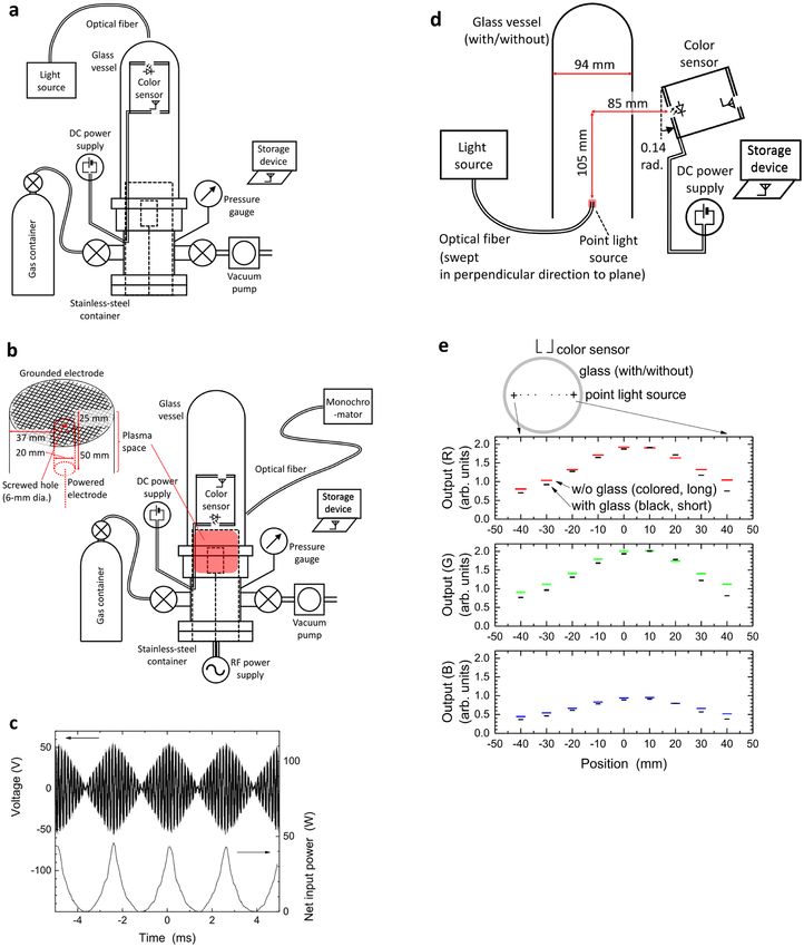
www.nature.com/scientificreports/
Figure 1. Conceptual view of edge-computing and wireless-communication system used in this study with a
block diagram of the electronics in the colour sensor.
We also designed our in situ sensor for robustness in low-pressure operation, which is an abnormal and very
unlikely situation for classical sensors used in daily life. Our goal is to design a sensor for operation inside the
vacuum chambers, because parameters of events inside the chambers are usually recorded using probing meth-
ods that are classically limited to analogue sensing and tend to suffer from noise interference. For instance, an
optical probing device used for diagnostics of plasma in low-pressure vacuum chambers usually operates from
outside through glass windows3,13–15. Light emissions from plasma are spatially integrated, leading to low spatial
resolution3, and attenuated through the plasma itself and the window; ambient background noise easily sneaks
into the signals detected by outside sensors. If we include robustness against low-pressure conditions, mainly by
removing the possibilities of evaporation and/or explosion of constituents16 in the hardware components, then we
can use these sensors inside vacuum chambers. When we directly detect light emissions from plasma, signals are
free from the attenuation and contamination of background noise, while spatial signal integration is minimized.
In this context, our proposed scheme shares several points with the Internet of Things (IoT)17–20. Due to
recent progress in IoT technology, large amounts of data are accumulated and available in healthcare systems,
environmental monitoring systems, structural health monitoring systems, etc. This IoT technology basically
handles the connections of things to the Internet or wireless communication networks. Our sensors are similar to
IoT devices such as advanced sensors and their data acquisition s ystems2. In our case, we focus on the extension
of sensor locations to an extreme environmental condition. Similar concepts were partially achieved in space
science for satellites and planet probes21–24, but the expense and complexity of these probes are too specific for
application to daily activities or for large-scale factory manufacturing.
In this study, we designed an in-vacuum active optical sensor that is capable of in situ computing and installed
it in a vacuum chamber to detect light signals. The sensor consists of an integrated photodiode sensor with red
(R), green (G), and blue (B) sensitivities and interintegrated circuit outputs, a reduced-instruction-set-computer
(RISC) single-chip microcontroller, and a Bluetooth module (IEEE 802.15.1)25, all of which are commercially
available at fairly low cost. Using this sensor at approximately 30 Pa in a vacuum chamber, we successfully
monitored RGB intensities in the visible light range while recording the data to a personal computer outside
the chamber (in ambient air at atmospheric pressure). After plasma ignition at 100 Pa of Ar, we observed direct
optical signals from plasma emissions, and the detected values were considered reasonable responses based
on the external parameter settings. The detected signals, completely without filtering effects in their output
numerals, included information on the excited states of the Ar gas in the plasma region, which is indicated in
an energy-level network diagram.
Sensor operation in low‑pressure vacuum chamber
The in-vacuum active sensor possesses RGB-signal sensitivities, computing capability, a wireless communica-
tion function, and robustness at low pressure, as shown in Fig. 1 and described in the “Methods” section. In
brief, an integrated photodiode array monitors the three colour components and creates three digital numeral
outputs after A/D conversion, and the RISC microcontroller handles these outputs and sends them via Bluetooth
standard wireless communication to a master personal computer that requests data transfer from the sensor. We
stress that these circuit components for the vacuum chamber operation are commercially available at low cost
without the need for custom orders. All the circuit components are in a metallic (aluminium) container with
one side open for light introduction and another for wireless communication. Accurate calibration of these RGB
outputs is completed after the procedure, and we had previously developed a supervised-learning calibration
Scientific Reports | (2021) 11:1364 | https://doi.org/10.1038/s41598-020-80501-z 2
Vol:.(1234567890)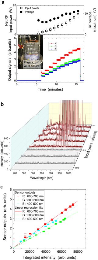
www.nature.com/scientificreports/
Figure 2. Output signals of the sensor when light originates from the halogen lamp located outside the
chamber and enters the sensor inlet through the glass vessel. (a) Time evolution of the signals detected by
the optical sensor located in the pressure-varying chamber. A bandpass filter with a centre wavelength of
550 nm is inserted on the outlet of the optical fibre that guides light from the lamp. (b) Signals of the R, G, and
B components as a function of the centre wavelength bandpass filter. The halogen lamp emission spectrum
detected by the monochromator is also shown. The values shown here are approximately 200 Pa, although they
are invariant, as shown in (a), regardless of pressure.
method using more than 1,600 colour samples26. However, we used these raw RGB outputs for comparison with
wavelength spectra, as described below.
We installed sensors in two different setups in the same vacuum chamber; the lower part was made of stain-
less steel, whereas the upper part was a fused-quartz vessel (see details in the “Methods” section and Ref.27).
For confirmation of invariances in the electronic device functions at low pressure, we used the glass-vessel part
with no colour and enough transparency to allow us to test both the light detection and wireless communica-
tion. The glass vessel had a 100-mm outer diameter, larger than that in our previous e xperiment27. In the lower
part, a columnar discharge electrode was set on the bottom with a metal-mesh-facing grounded electrode (see
“Methods”).
After installing the sensor above the grounded electrode and pumping the gas to 30 Pa, we tested for light
detection and wireless communication as described below. This pressure is similar to or lower than that used
for the plasma-enhanced chemical vapor deposition of thin Si films28 but higher than that for dry etching for
trench formation in Si-oriented thin films29,30. Figure 2a shows signals transferred to the storage device outside
the chamber, where visible lights were controlled by a halogen-lamp light source (Megalight100, SCHOTT Japan
Corp.) externally installed above the glass vessel with wavelength bandpass filters (TS OD 4, Edmund Optics
Ltd.). During the total operation period, the detected signals remained constant except for a slight reduction
in the transient intensity of the light source during its start-up phase, indicating that the sensor suffered from
neither a functional disorder nor a deterioration in signal level. We also confirmed that there were no effects
of possible outgas from the sensors following the successful invariant operation at low pressure; no change in
pressure trend occurred after pumping began or during the phases in which the pressure was decreased to 30 Pa
or elevated up to that of air. This indicates that the electronic circuits, including the three chips of the integrated
Scientific Reports | (2021) 11:1364 | https://doi.org/10.1038/s41598-020-80501-z 3
Vol.:(0123456789)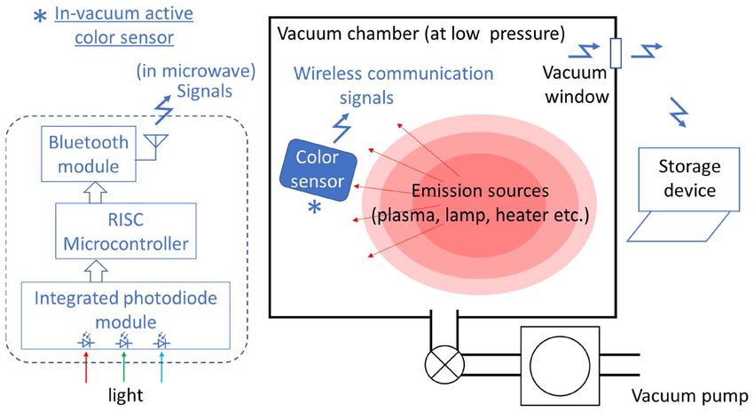
www.nature.com/scientificreports/
circuits, were live without any functional degradation during the operation of the vacuum pump. If any enclosed
gas bubbles remained in the chips, they would have exploded at low pressure and might have damaged the fine
circuit patterns, but this was not the case. Another concern is vapor evaporation of some parts of the circuits
or other protection layers, but we confirmed sufficient robustness of our device because, as indicated above, we
observed neither deterioration in sensor output nor abnormal pressure elevation during our tests.
Figure 2b shows the wavelength sensitivities of the R, G, and B sensor outputs by changing the centre wave-
length of the bandpass filters. Although the range of each output has its own wavelength dependence, rough
estimations suggest that the R component corresponds to lights from 600 to 700 nm, the G component from 500
to 600 nm, and the B component from 400 to 500 nm.
Direct detection of plasma light emissions
Plasma in an electric discharge emits visible/ultraviolet/infrared lights spontaneously according to the excited
energy levels of the included gases. Many articles have reported the results of optical diagnostics of plasma emis-
sions obtained thus far, and almost all measurements were performed through layers or media such as vacuum
windows, optical fibres, optical lenses/filters, and gas layers outside the plasma regions13–15. Careful preparation
and arrangement of these layers can assure suitable (or equivalent) transparency for light. However, we cannot
completely remove the possibility of signal degradation arising from surface reflections or wavelength dispersions
of the optical components3–7 (see “Methods”). In addition, gas layers may induce self-absorption that reduces the
original light i ntensity31. Direct measurements with optical sensors placed inside or in proximity to the plasma
are favourable for the elimination of these concerns, and were considered for our proposed system.
To perform our experiments with the colour sensor placed in the plasma space at low pressure, we installed
the sensor upside down on the case, as shown in Fig. 2 (see “Methods”), with plasma generated on the lower
side of the grounded mesh electrode and the plasma emissions moving along a direct path to the sensor inlet
surface (the distance from the edge of the plasma was only 10 mm). To confirm that the plasma signals are dis-
tinguished from the background level (which was zero for all R, G, and B colour components), we adjusted the
radiofrequency (RF) input power for plasma generation stepwise, by varying every 0.01-V output voltage of the
RF signal generator and observed the corresponding responses. Figure 3a shows the detected signals over time.
The signals started up at the sixth step, which was exactly the same time of the plasma ignition and demonstrated
the same stepwise behaviour as that of the input power.
Before confirming the accuracy of the sensor signals, we investigated possible analogue noise signals on
the signal processing unit. When we triggered analogue signals in a vacuum chamber, transmitted them to the
storage device, and converted them to digital numerals, significant levels of noise invaded the estimated signal
values. Figure 3a shows the RF voltage detected on the transmission line established between the RF amplifier
and the powered electrode. This voltage is approximately the maximum level of the electric potential in the loca-
tion of the sensor in this experiment. The voltage on the powered electrode, which was the ending point of the
RF transmission line, was similar to or somewhat enhanced from the observed amplitude due to the mixing of
forward and reflected RF powers. The plasma potential was similar to this externally-applied voltage because a
sheath was mainly created on the surface of the grounded electrode. The mesh structure of the grounded electrode
may sufficiently suppress this sheath potential, but part of it reaches the sensor since plasma leaked through the
mesh holes (3.0 by 3.0 mm2). These considerations and findings imply that this in situ sensor significantly sup-
pressed the noise effects created by the A/D conversion in the edge computing function; otherwise, the analogue
data detected on the sensor would include RF noise attacking the signal transmission paths and might make
the signals ambiguous.
To specify the sources of these sensor output signals, we simultaneously detected wavelength spectra of visible
lights picked up by the optical fibre on the outer surface of the glass vessel, on the air side, and monitored it with
a monochromator (USB4000, Ocean Optics Ltd.). As shown in Fig. 3b, the main emissions from the Ar plasma
were in the infrared-ray range, but we also observed many spectra in the visible light range. These spectra indicate
gradual changes in intensities in a manner similar to those of the elevated power levels for plasma generation.
For a rough comparison, we plotted each output component of our in situ colour sensor as a function of the
integrated values in the corresponding wavelength ranges (R for the range from 600 to 700 nm, G for that from
500 to 600 nm, and B for that from 400 to 500 nm (Fig. 3c). All dependences are clearly along one line of linear
regression. This coincidentally confirmed that the output signals of the sensor successfully reflected Ar plasma
emissions in this low-pressure in situ situation.
One may consider that these R, G, and B signals have wavelength resolutions too broad to determine what
happens inside plasma. However, these signals provide significant information on the balance of neutral atoms
in the plasma at excited states. Ar I emissions arising from the excited levels of Ar atoms include 428 spectra, all
listed in Ref.32, expanding from the ultraviolet (UV) to middle infrared ranges. The list of transitions between
quantum levels, unique to each atom species, is too complicated for intuitive understanding (see the supple-
mental file). However, we can obtain clearer insight by using a graphic representation with nodes representing
excited levels and edges representing transitions (Fig. 4a), such as the expressions of complex chemical systems in
molecular plasmas33–35. For instance, spectra in the R component (from approximately 600 to 700 nm) originate
primarily from the transitions from the 3s23p55d’ to 3s23p54p group in the Racah notation.
Generally, with some overlapping areas, transitions yielding emissions for the B, G, and R components are
divided by area in this graphic representation. Using L and U for lower and upper energy levels for emissive
transitions in the subscripts of group names, we obtain an overview of the energy transitions in Ar I emissions.
The area for BU is shown in the lower-left part of Fig. 4a, in which nodes representing the upper levels of energy
for emissions from 400 to 500 nm are present and superposed with the ultraviolet (UV) region. The area for GU is
on the right-hand side and that for R U is shown mostly in the upper part of Fig. 4a. Area B U shares a partial area,
Scientific Reports | (2021) 11:1364 | https://doi.org/10.1038/s41598-020-80501-z 4
Vol:.(1234567890)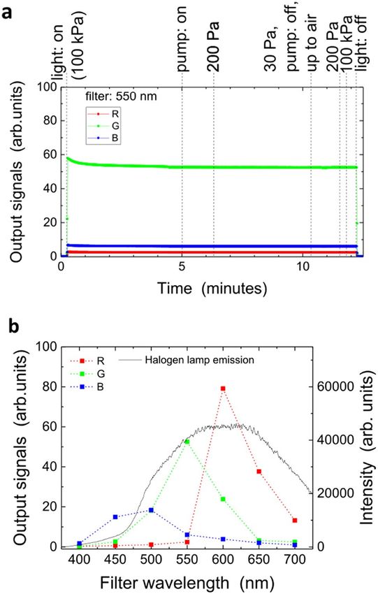
www.nature.com/scientificreports/

                                  Figure 3.  Detection of plasma emissions at 100 Pa of Ar. (a) Time evolutions of signals of averaged radiofrequency (RF,
                                  13.56 MHz) net input power for plasma generation with the corresponding peak RF amplitude (upper side) and R, G, and
                                  B outputs of the sensor located in the vicinity of the plasma region (lower side), recorded on a personal computer located
                                  outside the vacuum chamber. Input power is linearly elevated every minute, and the power at level six ignites plasma. The inset
                                  photograph shows the outlook of the vacuum chamber used here and the visible plasma image. (b) Emission spectra of plasma
                                  monitored by monochromator to which optical fibre transmits lights from other end located just outside of glass vessel.
                                  Spectrum examples before plasma ignition are in grey, whereas those after plasma ignition are in brown, and lower-level
                                  signals are enlarged to focus on intensities in the visible light range. (c) Comparison of sensor output signals with integrated
                                  intensities of spectra monitored by monochromator. The signals used here are shown in (a).

Scientific Reports |   (2021) 11:1364 |                  https://doi.org/10.1038/s41598-020-80501-z                                                             5

                                                                                                                                                          Vol.:(0123456789)
www.nature.com/scientificreports/
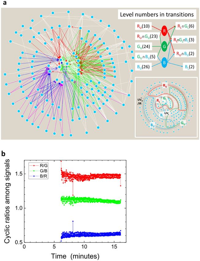
Figure 4. Information on the R, G, and B outputs of the sensor. (a) Transitions of Ar I emissions listed in the
literature32 (see Supplemental File). Nodes represent energy levels, and directed edges indicate transitions using
the colour of each output component of the sensor. We assume that wavelengths from 400 to 500 nm, from 500
to 600 nm and from 600 to 700 nm correspond to B, G, and R components, and subscripts U and L indicate
upper and lower energy levels in transitions. Node groups and their node numbers are shown on the right side.
(b) Ratios of R to G, G to B, and B to R of data in Fig. 3a.
corresponding to five nodes, with GU. Areas GU and RU share 23 nodes, but areas BU and RU share no nodes. The
numbers of the lower levels for the R, G, and B components are much smaller, limited to 12 nodes, and many of
these nodes are shared by the BL, GL, and R L groups. We found three exceptions that cannot be included in the
preceding description. One level in the R U group also serves as a lower level for an emission in the R component,
and another level in the R
U and G
U mixed group serves also an upper level for an emission from the R component.
The remaining exceptional fact is that we observed one H-atom emission spectrum at 656.2 nm (in Fig. 3b and
the Supplemental File), which is probably due to H 2O impurities and contributes slightly to the R component.
However, the main system of optical emissions consists of groups of upper (RU, GU, and B U) and lower (RL, GL,
and BL) levels and their crossing directed links.
By detecting ratios among the three components, we can judge which part shown in Fig. 4a is more active
during transitions inside plasma. Figure 4b shows the ratios of components R to G, G to B, and B to R detected by
the sensor in the low-pressure chamber, as shown in Fig. 3a. For 10 min, the changes in signals were complicated,
Scientific Reports | (2021) 11:1364 | https://doi.org/10.1038/s41598-020-80501-z 6
Vol:.(1234567890)www.nature.com/scientificreports/
which may reflect a stabilization stage of the plasma structure. After 10 min, the input power caused the plasma
parameters to vary monotonically. The ratio of R to G was constant during this phase; notably, the R and G
components share many upper energy levels, making this constant tendency reasonable. The ratio of B to R
increases, and that of G to B decreases; these two dependences indicate enhancement of a relative increase of the
B component. In fact, as shown in Fig. 3b, the intensities of the transitions from 3s23p55p’ to 3s23p54s at 415.8591,
419.8317, and 420.0675 nm increased correspondingly.
In this experiment, we set the colour sensor to detect plasma emissions while comparable data monitored
by a monochromator were available from the same equipment. We successfully confirmed the validity of the
operation at low pressure and the data accumulation outside the vacuum chamber and found reasonable agree-
ment of both datasets. At this point, this sensor was ready for use in a larger vacuum chamber with plasmas and/
or other light emitting objects, which were unobservable from outside the vacuum chambers. The sensor uses
paths through small vacuum windows for data transfer by wireless communication and installing colour sensors
allowed us to visualize phenomena at low pressure inside the industrial vacuum chamber systems. According to
the most rigorous definition, this sensor is not an edge computing device with local and flexible intelligence8–12
but is equivalently capable of in situ computing. Such in situ data processing for accurate data acquisition is a
promising trend for scientific and industrial sensor systems that allow us to secure a large amount of reliable data.
Concluding remarks
In this study, we demonstrated that our in-vacuum active colour sensor successfully detected direct optical lights
emitted from discharge plasma under the low-pressure conditions of a vacuum chamber, computed analogue
signals to digital numerals, and sent them to a storage device located outside the chamber. The capability of the
colour sensor was invariant in cases where the gas pressure of its location, 30 Pa, varied from the atmospheric
pressure, and we observed no significant outgases caused by possible detachment from the sensor surface, as
long as we investigated them with a typical gas-pressure gauge. Its capable function did not vary even when
the plasma was ignited at a position 10 mm away from the sensor, and the sensor successfully detected plasma
emission signals as R, G, and B components of the output. This low-cost and easy-to-install sensor can provide
useful data on the raw emission signals of the balance between excited energy states of discharge gases in the
out-of-reach regions of plasma reactors without any filtering effects.
Methods
Design of the in‑vacuum active sensor. Our in-vacuum active sensor is composed of printed circuit
boards, discrete electronic circuit devices, and a sealing container. The required features in the entire sensing
system for our purpose are summarized in three elements: RGB sensitivities were captured by a tiny integrated
photodiode module, IoT capability enabled the data transfer from raw RGB digital bit-data through wireless
communications, and the active functions of the sensor and computing electronic devices were robust.
It is preferable for the in situ sensor to occupy a small area or volume in the system that the device monitors;
therefore, we adopted an RGB colour sensor (S11059-02DT, Hamamatsu Photonics K.K.), which is an integrated
photodiode module chip with a sensitive area of 0.54 by 1.1 mm2. It accepts several commands including address
calls, register calls, and data read-outs, and sends 8-bit outputs for each component (R, G, or B). While several
types of colour-matching functions for wavelength spectra have been proposed36, we did not use the possible
corrections of RGB values as outputs of the sensor and used these raw data to confirm the direct measurements
on plasma emission information without any significant noise contamination. Instead of rigorous calibration of
these data as R, G, and B values, we assured their linkage to chroma and hue values as described below26. We built
up a convenient RGB-sensitive colour detector (Color Checker CC-01, Checkers Co.) that included a white light
emitting diode (LED) with the same RGB colour sensor (S11059-02DT, Hamamatsu Photonics K.K.). This handy
system was used for the calibration of the RGB colour sensor, as described in Ref.26 and summarized below. We
performed supervised learning for two-layer neural networks using more than 1600 colour catalogue samples
(Pantone Formula Guide, Pantone LLC, X-Rite Inc.) as training data. The neural networks identified positions
on the CIE 1931 colour xy coordinates on which the values of chroma and hue were d efined36. In addition, we
linked the two counter colours, white and black, to the sensor outputs as shown below. We used a colourless,
blank part of a white Pantone catalogue sheet and coated it white because white colour can be defined as a
state with no absorption of reflected lights; the R, G, and B values in this test were set to zero. The black colour
is equivalent to a case with the signal levels when no reflector is installed for the sensor, as all the R, G, and B
lights are completely absorbed and their corresponding values in the sensor outputs are set to be the maximum.
Although both of these colours correspond to (x, y) = (0.333, 0.333) on the colour coordinate, the sensor outputs
are located at the very ends on both sides. Consequently, based on this assumption, it is possible to use this tiny
RGB colour sensor solely in our in-vacuum active device with the working standard calibration level1. The colour
sensor also has an infrared-ray (IR) signal whose spectrum has a peak wavelength of 855 nm and ranges from
785 to 885 nm, although its value is neither calibrated nor used in our experiment.
After receiving light and converting the light levels into numeral outputs in the photodiode array chip, a RISC
micro-controller (AVR Microcontroller MEGA88V, Atmel Corp.) sent the outputs in nine bits via Bluetooth
standard wireless communication to a master personal computer that sends data-transfer request messages to
the sensor. Additionally, this RISC micro-controller includes the abovementioned calibration procedure for
optimized two-layer neural networks. Another chip (ADM3202, Analog Devices Inc.) performed the Bluetooth
wireless communication. All the circuit components were in a metallic (aluminium) container (70 × 20 × 83 mm3)
with an open perforated hole (260 m m2) for wireless communication. Bluetooth wireless communication between
inside sensors and outside data storage devices such as personal computers may be unstable or impossible if there
are not enough paths for microwaves of approximately 2.4 GHz. This difficulty can be overcome, as we recently
Scientific Reports | (2021) 11:1364 | https://doi.org/10.1038/s41598-020-80501-z 7
Vol.:(0123456789)www.nature.com/scientificreports/
successfully observed microwave cloaking in plasma s pace27,37–39, by detouring the signals around the metallic
components. This technique was not introduced in our system described here, although it is ready for practical
use by setting anisotropic metamaterials around the dielectric window that faces both the low-pressure plasma
space and the ambient air. The signals transferred to the personal computer are shown in its display and are
simultaneously stored in its memory every second in line with the evolutions of R, G, B, and IR signals with time.
A printed circuit board (PCB), which was a typical glass epoxy plate (FR-4, frame retardant type 4), held the
discrete devices with circuit connections composed of classical copper lines arranged by computer-aided design.
The surface finish was coverage of organic solderability preservative (OSP) on the Cu l ines40 and thin-film solder
mask on the other area; these finish layers prevent copper corrosion and, after a baking process of approximately
120 degrees Celsius, achieve high thermal endurance that may repel the bombardment of plasma particles. The
maximum temperature was fixed at a working temperature of 80 degrees Celsius for the RGB colour sensor,
which tolerated the installation of the metallic-sealed sensor system on the vacuum chamber wall, which contacts
the ambient air at room temperature even when a heater for the substrates, etc., is used somewhere else in the
chamber. The electronic circuit’s power supply was directed from outside the chamber through a vacuum-sealed
connector; however, battery technology for satellites was sufficient for our purpose41. Recently, lithium-ion bat-
teries have also been available for this purpose, since, before commercial use, they have been tested under the
UN/DOT 38.3 regulation, which stipulates that endurance at a pressure of 11.6 kPa or less is required for aircraft
equipment42. The pressure difference of the test and the ambient environment (100 kPa) was approximately
88 kPa, which is only slightly less than that in our case (~ 100 kPa). One electrolyte-filling process method for
lithium-ion batteries is performed under low pressure in a vacuum c hamber43,44, which indicates that inclusion
of these batteries in a vacuum chamber is possible.
Experimental setup of vacuum chamber. We used a compact vacuum chamber made of a stainless
steel container and a fused-quartz glass vessel for the experiments, which were the common components previ-
ously reported27. The inset photograph in Fig. 3a shows a partial view of the chamber and the specific chamber
configuration is shown in Fig. 5. The chamber wall of the upper part was fused-quartz glass through which both
visible light and microwaves can penetrate it, with an outer diameter of 100 mm at 3-mm thickness. As shown in
Fig. 5a, this upper part is useful for detection of the externally-supplied light source. The light from the halogen
lamp was injected from the top of the glass vessel and due to optical transparency, the colour sensor detected
the light with almost no depression. The glass vessel is also transparent for Bluetooth signals at approximately
2.4 GHz, which allows the microwave to propagate freely between the sensor in the chamber and the storage
device outside the chamber. The lower part was enclosed by a stainless-steel wall and works only for adjustment
of gas pressure, which depends on the balance between the openings of two valves for the gas-feed inlet and
outlet.
The main function of the lower part of the chamber was room for plasma, as shown in Fig. 5b. A cylindrical
grounded electrode made of a thin aluminium plate covered its inner surface with a diameter of 94 mm, which
was electrically continuous to the metallic mesh electrode on the top side of this cylinder (Fig. 5b). Inside this
metallic cylindrical shell, we installed a powered metallic electrode made of stainless steel whose diameter was
20 mm with a 6-mm screw hole. The distance between the powered and the grounded metallic mesh electrodes
was 25 mm, whereas that on the side of the powered electrode was 37 mm. This spatial configuration sup-
ports two-discharge geometry; one is discharge between the powered and grounded electrodes, and the other
is hollow-cathode d ischarge45 mainly generated in the screw hole. As shown in Fig. 3a, both discharge regimes
were observed and sufficient emissions of visible light with high signal-to-noise ratios enabled us to confirm the
validity of this measurement system. As in the experiments of the externally provided light detection, the sensor
was installed in the upper part of the chamber, i.e. in the glass vessel, but its optical inlet was to the lower side to
detect plasma emissions. Due to the transparency of the upper part, we can expect smooth wireless communica-
tion and monochromator measurements of visible emissions from inside to outside.
The method for supplying power for plasma generation was a classical one: a signal generator (WF1974, NF
Corporation) of an RF wave at 13.56 MHz amplified by 55 dB by an RF amplifier (T145-5546A, Thamway Co.,
Ltd). We then transferred the RF power with several tens of watts into the vacuum chamber through the match-
ing circuit with parallel and series capacitors with a series inductor. The temporal envelope of the power input
was in the shape of a triangle at 400 Hz (Fig. 5c). A 40-dB directional coupler (T051-5726A, Thamway Co., Ltd)
located between the output of the amplifier and the powered electrode monitored forward and reflected power
levels. The gas inlet and outlet valves were on the sides of the chamber on the respective opposite directions, and
the Ar gas at 20 mL/min flowed with its pressure set to 100 Pa by adjusting the opening ratio of the outlet valve,
which was connected to an oil-sealed rotary-vane vacuum pump. Gas pressure was monitored by a thermocouple
vacuum gauge (M-012DM, Canon Anelva Corporation).
Figure 5c shows an example of the RF signals monitored in one parameter (level 15, the maximum in our
experiments). The RF forward voltage was detected by the directional coupler. The net input power was calcu-
lated from the forward power component from which the reflected power was subtracted. In Fig. 3, we plotted
the average values of the net input power.
As aforementioned, the fused-quartz glass vessel was sufficiently transparent to visible light, but it deformed
light signals from the inner space (e.g., plasma emission in this study) when we installed our in-vacuum colour
sensor outside the vessel as in the conventional manner. To confirm the advantage of inner installation for data
acquisition, we performed an experiment of light detection in the setup shown in Fig. 5d at atmospheric pressure
and compared the results. In this case, light emission from the optical fibre outlet imitated the local plasma emis-
sion from the corresponding spatial point. As we swept the optical fibre, when the point light source at locations
near the vessel wall, the profiles of the signals detected outside the vessel were depressed due to nonuniform
Scientific Reports | (2021) 11:1364 | https://doi.org/10.1038/s41598-020-80501-z 8
Vol:.(1234567890)www.nature.com/scientificreports/
Figure 5. Setups of the vacuum chamber with colour sensor installation. (a) Detection of externally-controlled
light. The data in Fig. 2 are obtained in this setup. (b) Detection of Ar plasma emissions. The data in Fig. 3 are
obtained from this setup. (c) Example time evolutions of radiofrequency signals: forward voltage monitored
by a directional coupler located before the powered electrode (upper side) and net input power (lower side).
(d) Identification of the difference between direct (without glass) and indirect (with glass) sensing. (e) Colour
sensor signals in direct and indirect measurements in the setup shown in (d).
Scientific Reports | (2021) 11:1364 | https://doi.org/10.1038/s41598-020-80501-z 9
Vol.:(0123456789)www.nature.com/scientificreports/
glass refraction and surface reflection of the light, while those in the centre were unchanged (Fig. 5e). Curva-
tures in glass or other obstacles, such as contaminated surfaces, are likely to affect the light signals, but no signal
change occurred when we set our colour sensor inside the vacuum vessels or chambers. Our concept of colour
sensor installation in a vacuum to detect inside light is definitely superior to sensors sitting outside a vacuum
container because, in the vacuum, no absorber, reflector, or refractive medium exists between the light source
and the colour sensor.
Received: 16 March 2020; Accepted: 16 December 2020
References
1. Northrop, R. B. Introduction to Instrumentation and Measurements (CRC Press, London, 2005).
2. Mukhopadhyay, S. C. Intelligent Sensing, Instrumentation and Measurements (Springer, New York, 2013).
3. Hutchinson, I. H. Principles of Plasma Diagnostics (Cambridge University Press, Cambridge, 2002).
4. Sommerfeld, A. Lectures on Theoretical Physics: Optics (Academic Press, New York, 1964).
5. Lipson, A., Lipson, S. G. & Lipson, H. Optical Physics 4th edn. (Cambridge University Press, Cambridge, 2010).
6. Pozar, D. M. Microwave Engineering (Addison-Wesley, London, 1990).
7. Swanson, D. G. Plasma Waves (Academic, New York, 1989).
8. Satyanarayanan, M., Bahl, V., Caceres, R. & Davies, N. The case for vm-based cloudlets in mobile computing. IEEE Pervasive
Comput. 1, 2–11 (2009).
9. Shi, W. & Dustdar, S. The promise of edge computing. Computer 49, 78–81 (2016).
10. Satyanarayanan, M. How we created edge computing. Nat. Electron. 2, 42 (2019).
11. Khan, W. Z., Ahmed, E., Hakak, S., Yaqoob, I. & Ahmed, A. Edge computing: A survey. Future Gener. Comput. Syst. 97, 219–235
(2019).
12. Passian, A. & Imam, N. Nanosystems, edge computing, and the next generation computing systems. Sensors 19, 4048 (2019).
13. Zhu, X. M. & Pu, Y. K. Optical emission spectroscopy in low-temperature plasmas containing argon and nitrogen: Determination
of the electron temperature and density by the line-ratio method. J. Phys. D: Appl. Phys. 43, 403001 (2010).
14. Sakai, O., Kimura, M., Shirafuji, T. & Tachibana, K. Underwater microdischarge in arranged microbubbles produced by electrolysis
in electrolyte solution using fabric-type electrode. Appl. Phys. Lett. 93, 231501 (2008).
15. Urabe, K. & Sakai, O. Multiheterodyne interference spectroscopy using a probing optical frequency comb and a reference single-
frequency laser. Phys. Rev. A 88, 023856 (2013).
16. Kittel, C. Thermal Physics (Wiley, New York, 1969).
17. Gershenfeld, N., Krikorian, R. & Cohen, D. The Internet of things. Sci. Am. 291, 76–81 (2004).
18. Kranz, M., Holleis, P. & Schmidt, A. Embedded interaction: Interacting with the internet of things. IEEE Internet Comput. 14,
46–53 (2010).
19. Atzori, L., Iera, A. & Morabito, G. The internet of things: A survey. Comput. Netw. 54, 2787–2805 (2010).
20. Tokognon, C. J. A., Gao, B., Tian, G. Y. & Yan, Y. Structural health monitoring framework based on Internet of things: A survey.
IEEE Internet Things J. 4, 619–635 (2017).
21. Kuenzera, C. et al. Earth observation satellite sensors for biodiversity monitoring: Potentials and bottlenecks. Int. J. Remote Sens.
35, 6599–6647 (2014).
22. Chandera, G., Markham, B. L. & Helder, D. L. Summary of current radiometric calibration coefficients for Landsat MSS, TM,
ETM+, and EO-1 ALI sensors. Remote Sens. Environ. 113, 893–903 (2009).
23. Lebreton, J. P. et al. An overview of the descent and landing of the Huygens probe on Titan. Nature 438, 758–764 (2005).
24. Abe, M. et al. Near-infrared spectral results of Asteroid Itokawa from the Hayabusa spacecraft. Science 312, 1334–1338 (2006).
25. Bluetooth technology by Bluetooth SIG, Inc. in https://www.bluetooth.com
26. Ueno, S. & Sakai, O. Low-cost color-sensitive optical sensor and its calibration by neural network. in Proceedings of the 2019 IEEE
8th Global Conference on Consumer Electronics 1180–1181 (Osaka, Japan, 2019).
27. Sakai, O. et al. Plasma metamaterials as cloaking and nonlinear media. Plasma Phys. Control. Fusion 59, 014042 (2017).
28. Perrin, J. Reactor design for a-Si:H deposition. in (Bruno, G., Capezzuto, P. & Madan A. eds.) Plasma Deposition of Amorphous
Silicon-Based Materials. (Academic Press, 1995).
29. Coburn, J. W. & Winters, H. F. Ion and electron assisted gas surface chemistry—An important effect in plasma etching. J. Appl.
Phys. 50, 3189–3196 (1979).
30. Hitchon, W. N. G. Plasma Processes for Semiconductor Fabrication 121–142 (Cambridge University Press, Cambridge, 1999).
31. Djurovic, S., Pelaez, R. J., Cirišan, M., Aparicio, J. A. & Mar, S. Stark widths of Xe II lines in a pulsed plasma. J. Phys. B: At. Mol.
Opt. Phys. 39, 2901–2916 (2006).
32. NIST (National Institute of Standards and Technology, U.S. Department of Commerce) database in https://www.nist.gov/pml/
atomic-spectra-database
33. Sakai, O., Nobuto, K., Miyagi, S. & Tachibana, K. Analysis of weblike network structures of directed graphs for chemical reactions
in methane plasmas. AIP Adv. 5, 107140 (2015).
34. Mizui, Y., Nobuto, K., Miyagi, S. & Sakai, O. Complex reaction network in silane plasma chemistry. in Complex Networks VIII
135–140 (Springer, 2017).
35. Mizui, Y., Kojima, T., Miyagi, S. & Sakai, O. Graphical classification in multi-centrality-index diagrams for complex chemical
networks. Symmetry 9, 309 (2017).
36. Hunt, R.W.G. & Pointer, M.R. Measuring Colour 4th edn 20–40. (Wiley, 2011).
37. Iwai, A., Nakamura, Y. & Sakai, O. Enhanced generation of a second-harmonic wave in a composite of metamaterial and microwave
plasma with various permittivities. Phys. Rev. E 92, 033105 (2015).
38. Bambina, A., Yamaguchi, S., Iwai, A., Miyagi, S. & Sakai, O. Size validity of plasma-metamaterial cloaking monitored by scattering
wave in finite difference time-domain method. AIP Adv. 8, 015309 (2018).
39. Naito, T., Tanaka, T., Fukuma, Y. & Sakai, O. Electromagnetic wave cloaking and scattering around an antiresonance-resonance
symmetrical pair in the frequency domain. Phys. Rev. E 99, 013204 (2019).
40. Eilbeck, W. J., Holmes, F., Taylor, C. E. & Underhill, A. E. Cobalt(II), nickel(II), and copper(II) complexes of 2-methylimidazole.
J. Chem. Soc. A 1968, 128–132 (1968).
41. Hill, C. A. Satellite battery technology—A tutorial and overview. IEEE Aerosp. Electr. Sys. Mag. 26, 38–43 (2011).
42. Recommendations on the Transport of Dangerous Goods. (United Nations, 2017) https://www.unece.org/fileadmin/DAM/trans/
danger/publi/manual/Rev.6/ST-SG-AC10-11-Rev6-Amend1e.pdf . Accessed 20 Dec 2019.
43. Wu, M. S., Liao, T. L., Wang, Y. Y. & Wan, C. C. Assessment of the wettability of porous electrodes for lithium-ion batteries. J. Appl.
Electrochem. 34, 797–805 (2004).
Scientific Reports | (2021) 11:1364 | https://doi.org/10.1038/s41598-020-80501-z 10
Vol:.(1234567890)www.nature.com/scientificreports/
44. Schilling, A., Gumbel, P., Moller, M., Kalkan, F., Dietrich, F., & Droder, K. X-ray based visualization of the electrolyte filling process
of lithium ion batteries. J. Electrochem. Soc. 166, A5163–A5167 (2019).
45. Lidsky, L. M., Rothleder, S. D., Rose, D. J. & Yoshikawa, S. Highly ionized hollow cathode discharge. J. Appl. Phys. 33, 2490–2497
(1962).
Acknowledgements
We thank S. Ueno at Checkers Co., Ltd., for his comments on sensor calibration. This study is supported in part
by the Strategic Information and Communications R&D Promotion Programme (SCOPE) from the Ministry of
Internal Affairs and Communications, Japan, and by a Grant-in-Aid for Scientific Research from the Japanese
Ministry of Education, Culture, Sports, Science and Technology (MEXT/JSPS KAKENHI) with Grant Numbers
JP18H03690.
Author contributions
O.S. supervised the research, proposed the basic concept, performed the experiments and network analysis on
the Ar energy transitions, and contributed to the writing of this paper. T.K. worked on sensor design and manu-
facturing, and performed the experiments. K.S. performed experiments, analysed the data, and contributed to
the writing of this paper. G.I. designed the microwave communication and detection systems. S.M. prepared the
data analysis environment and discussed the validity and implications of the experimental data. K.N. worked on
the sensor design. K.T. proposed the outline of the sensor design and its conceptual use in industrial applications.
Additional information
Supplementary Information The online version contains supplementary material available at https://doi.
org/10.1038/s41598-020-80501-z.
Correspondence and requests for materials should be addressed to O.S.
Reprints and permissions information is available at www.nature.com/reprints.
Publisher’s note Springer Nature remains neutral with regard to jurisdictional claims in published maps and
institutional affiliations.
Open Access This article is licensed under a Creative Commons Attribution 4.0 International
License, which permits use, sharing, adaptation, distribution and reproduction in any medium or
format, as long as you give appropriate credit to the original author(s) and the source, provide a link to the
Creative Commons licence, and indicate if changes were made. The images or other third party material in this
article are included in the article’s Creative Commons licence, unless indicated otherwise in a credit line to the
material. If material is not included in the article’s Creative Commons licence and your intended use is not
permitted by statutory regulation or exceeds the permitted use, you will need to obtain permission directly from
the copyright holder. To view a copy of this licence, visit http://creativecommons.org/licenses/by/4.0/.
© The Author(s) 2021
Scientific Reports | (2021) 11:1364 | https://doi.org/10.1038/s41598-020-80501-z 11
Vol.:(0123456789)You can also read