Integration of Epitaxial Systems for Electronics Applications - Julien Brault Université Côte d'Azur, CNRS, CRHEA, Valbonne, France - Summer ...
←
→
Page content transcription
If your browser does not render page correctly, please read the page content below
Integration of Epitaxial Systems for
      Electronics Applications
                    Julien Brault
 Université Côte d’Azur, CNRS, CRHEA, Valbonne, France
            e-mail: Julien.Brault@crhea.cnrs.fr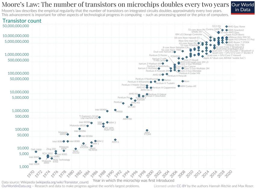
Nice
                                                               airport       Antibes

                   NICE

                                             CRHEA: Research Center for Hetero-
Sophia Antipolis: 30 000 jobs                Epitaxy & Applications
                                             (~ 60 pers., researchers, professors, students,
1200 companies / labs                        engineers, administratives)
•Research Labs (academic & private)
•Companies (medical, software, electronic,
numerical related to telecoms…)
Activities
EPITAXY
Semiconductors
(MBE, MOCVD)
Clean Room
Optical Char. Electrical Char.
Devices
PL, µ-PL, CL (I-V, Hall, C-V) (LEDs, HEMTs)
GaN : LEDs, µ-cavities, µ-lasers, electronics (RF, power) Structural Characterization
ZnO : IR, THz (QWIP, QCL), µ-cavities (polaritons) (X, AFM, SEM, TEM)
SiC : power electronics, buffer for GaN, MEMS
Graphene & 2D materials : CVD growth, VdW epitaxy
Metasurfaces: µ- / nano-fabrication on nitrides, oxides
3
Outline
Si Electronics
Si-based Technology: Field Effect Transistor, Metal-Oxide FET & CMOS Technology
From MOSFET to Integrated Circuits
Scaling: motivations & issues
Heterogeneous Integration & Defect Engineering
Heterogeneous Material Integration on Si Platforms
From MOSFET to HEMT
Epitaxy Defect Engineering
SiGe & III-V technology
Strained Si MOSFET
SiGe channels & III-V HEMTs
Nitride Materials – AlGaN/GaN HEMTs
Conclusions & perspectives
Pulse Summer School, Epitaxy Bases & Promises, Porquerolles, 2-8 July 2021 4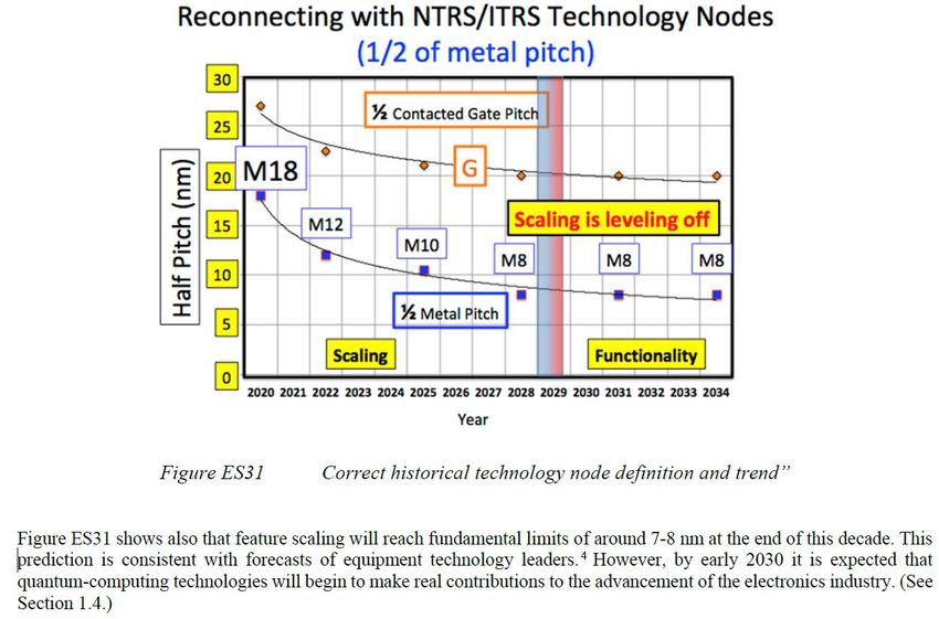
Si Electronics

                 Wednesday, July 7th 2021
                    Porquerolles, France    5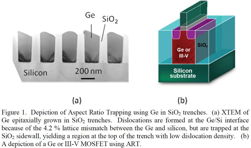
Si-based technology
Why Si ?
Silicon: abundant (2nd element (28%) after oxygen (46%)), cheap and simple purification process:
Reduction:
Silicon dioxide (SiO2) is reduced (@ 1500-2000 °C) : SiO2 + C → Si + CO2
Si is metallurgical grade silicon (MG-Si) 98-99% pure.
Presence of transition metals --> deep levels in the bandgap with high recombination activity -->
unsuitable for use in electronics https://www.pveducation.org/pvcdrom/
manufacturing-si-cells/refining-silicon
Purification in 2 steps:
- MG-Si is reacted with anhydrous HCl (@ 300 °C) to form SiHCl3: Si + 3HCl → SiHCl3 + H2
- SiHCl3 is reacted with hydrogen (@ 1100°C) to produce a very pure Si : SiHCl3 + H2 → Si + 3 HCl
Reaction inside large vacuum chambers & the Si is deposited
onto thin polysilicon rods to produce high-purity
polysilicon rods.
The resulting rods of semiconductor grade silicon are
broken up to form the feedstock for the crystallisation
process.
- Czochralski (CZ) process (Crystal pulling)
- Floating zone (FZ) process
Pulse Summer School, Epitaxy Bases & Promises, Porquerolles, 2-8 July 2021
Si wafers
Strong increase of the wafer diameter since the 1960’s
from 100mm to 300 mm
--> reduction of the price per transistor & performances improvement
Pulse Summer School, Epitaxy Bases & Promises, Porquerolles, 2-8 July 2021 7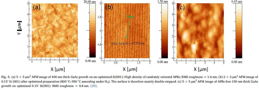
Field Effect Transistor
Transistor = SC device used to amplify or switch electronic signals and electrical power
A field effect transistor (FET) uses an electric field to control the flow of current & only
one kind of charge carrier
Amplifier = electronic device that can increase the power of a signal
Switch = electrical component that can disconnect or connect the conducting path
in an electrical circuit
First working device in 1947 by John Bardeen, Walter Brattain
« concept of a field-effect transistor » and William Shockley (Bell Labs)
Julius Edgar Lilienfeld
(1882 – 1963) Nobel Prize in Physics in 1956
Main type of transistor used = metal–oxide semiconductor
field-effect transistor (MOSFET)
invented by Mohamed Atalla and Dawon Kahng (1959, Bell Labs)
https://www.mksinst.com/n/mosfet-physics
Pulse Summer School, Epitaxy Bases & Promises, Porquerolles, 2-8 July 2021 8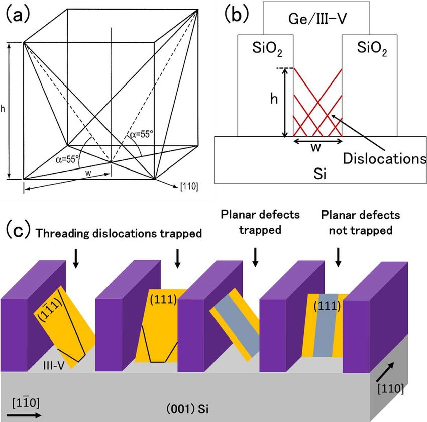
Metal–Oxide semiconductor FET (MOSFET)
https://www.elprocus.com/the-fabrication-process-of-cmos-transistor/
Basic MOSFET devices used metal as the gate material
(now poly-Si), silicon dioxide as insulator
(gate oxide) and Si as substrate.
The gate switches on and off by the transistor
with an electric field crossing the gate oxide
3 terminal device :
The Source, Gate, Drain and Body terminals. In general, the body is channel
in connection with the source terminal thus forming a three-terminal
device such as a field-effect transistor.
The functionality of MOSFET depends on the electrical variations in the channel along
with the flow of carriers (either holes or electrons).
The charge carriers enter into the channel through the source and exit via the drain.
The N-Channel MOSFET has an N-channel region NMOS PMOS
The P- channel MOSFET has a P- Channel region
https://www.mksinst.com/n/mosfet-physics
Pulse Summer School, Epitaxy Bases & Promises, Porquerolles, 2-8 July 2021 9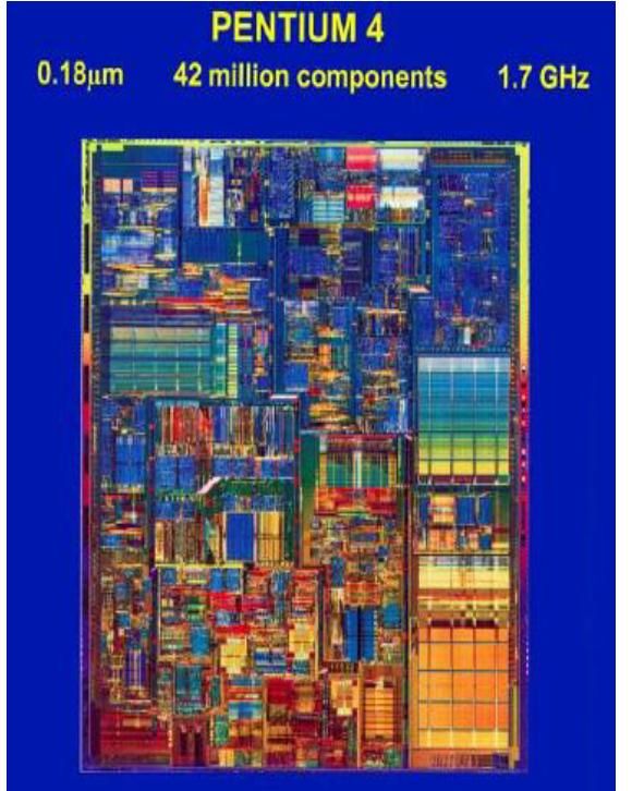
Metal–Oxide semiconductor FET (MOSFET)
Depletion mode and enhancement mode are two major transistor types:
- depletion = transistor in a normally-ON state
at zero gate-source voltage
- enhancement = transistor in a normally-OFF state
MOS Transistor main elements & process:
1. oxidation of the silicon substrate (field oxide) + etching part of the SiO2 ;
2. formation of a thin oxide layer (gate oxide–thermal oxidation) + deposition of poly Si (by CVD);
3. etching+doping (implantation) of Si creation of the source & drain junctions (self-aligned proc.);
4. insulating layer of SiO2 (by CVD) + etching (contact windows for source & drain) ;
5. deposition of the metal contact (Al) ; CMOS technology: complementary MOS
Gate
technology using both N and P channel devices
Poly Si oxide
Insulating poly-Si
oxide
oxide
source drain
http://emicroelectronics.free.fr/onlineCourses/VLSI/ch02.html
Pulse Summer School, Epitaxy Bases & Promises, Porquerolles, 2-8 July 2021 10Complementary metal–oxide–semiconductor (CMOS)
Advantages of CMOS: high noise immunity
& low static power consumption
CMOS technology is used to implement logic gates and other
digital circuits in integrated circuit (IC) chips, such as
microprocessors, microcontrollers, memory chips, and other
digital logic circuits.
CMOS technology is also used for analog circuits such as
image sensors (CMOS sensors), data converters,
RF circuits (RF CMOS), and highly integrated transceivers
for many types of communication.
https://en.wikipedia.org/wiki/CMOS#Logic
Pulse Summer School, Epitaxy Bases & Promises, Porquerolles, 2-8 July 2021 11MOSFET Characteristics (basics)
MOSFET are characterized by
2 electric field distributions in the structure:
The transverse field caused by the potential
difference between the gate and the source
(VGS). This field supports the substrate
depletion region (VGS < Vth) and
inversion layer (VGS > Vth).
The lateral field from source to drain potential
(VDS) --> main mechanism for current flow
in the MOSFET.
An inversion region with an
A depletion region excess of e- forms below the gate
@ zero or low VGS. oxide. This region connects the
No current flow source and drain N-type regions,
through the channel. forming a continuous N-region
from source to drain.
Pulse Summer School, Epitaxy Bases & Promises, Porquerolles, 2-8 July 2021 12MOSFET Characteristics (basics)
The output characteristics represents the drain current ID vs.
drain to source VDS for different values of gate to source voltage VGS V - V
GS th
The operation of MOSFET is used in
3 main regions:
- Cut-off region: the device will be in the
OFF condition and NO current flow through it
- Linear/Ohmic region: the current ID increases
linearly with the voltage VDS
- Saturation region: the drain to source current
value ID is constant & independent of VDS
IDSS
(the channel is pinched off at the drain side)
A 4th region occurs as VDS increases beyond
VDSS (saturation): the pinch off point moves
away from the drain by ∆L and has the effect
of changing the effective channel length in the transistor IDSS: maximum current flowing through
when the gate voltage VGS is 0V.
Pulse Summer School, Epitaxy Bases & Promises, Porquerolles, 2-8 July 2021 13MOSFET Characteristics (basics)
Linear/Ohmic region: In this region, the MOSFET works as an amplifier functionality.
The ability of MOSFET to amplify the signal is given by the output/input ratio:
--> transconductance gm = (dID/dVGS)VDS = VDSμWCi/L
µ = carrier mobility
L = gate length
W = gate width
Ci = gate insulator capacitance
High transconductance is obtained with high values of:
- the low field electron mobility (before saturation)
- thin gate insulator layers
(--> larger gate insulator capacitance ci = εi/di with
εi the permittivity and di the thickness of the gate dielectric)
- large W/L ratios
Pulse Summer School, Epitaxy Bases & Promises, Porquerolles, 2-8 July 2021 14MOSFET Characteristics (basics)
MOSFET used as an electronic switch (for controlling loads & in CMOS digital circuits).
They operate between the cut-off & saturation regions.
Cut-off region: VGS is low or zero, the channel resistance is very high & the transistor acts like an
open circuit --> no current flows through the channel. The MOSFET is “OFF” operating.
Saturation region: The ON-state gate voltage VGS ensures that the MOSFET is “ON” at a specific
drain current ID increases to its maximum value becomes constant independently of VDS and
depends only on VGS. The transistor is “ON” operating and behaves like a closed switch.
https://www.electronics-tutorials.ws/transistor/tran_7.html
Pulse Summer School, Epitaxy Bases & Promises, Porquerolles, 2-8 July 2021 15From Integrated Circuit…
IC = a set of electronic circuits on
one small flat piece (or "chip") of
semiconductor (Si)
The first monolithic IC was produced
on May 26th 1960
Fabrication of all the components
(transistors & resistances)
on a same wafer
by using oxide and Al contacts
¼ of 2-inch
Pulse Summer School, Epitaxy Bases & Promises, Porquerolles, 2-8 July 2021 16… to Microprocessor
First Microprocessor in 1971
(few thousands of MOS transistors)
Pentium 4 in 2000
(42 millions of components)
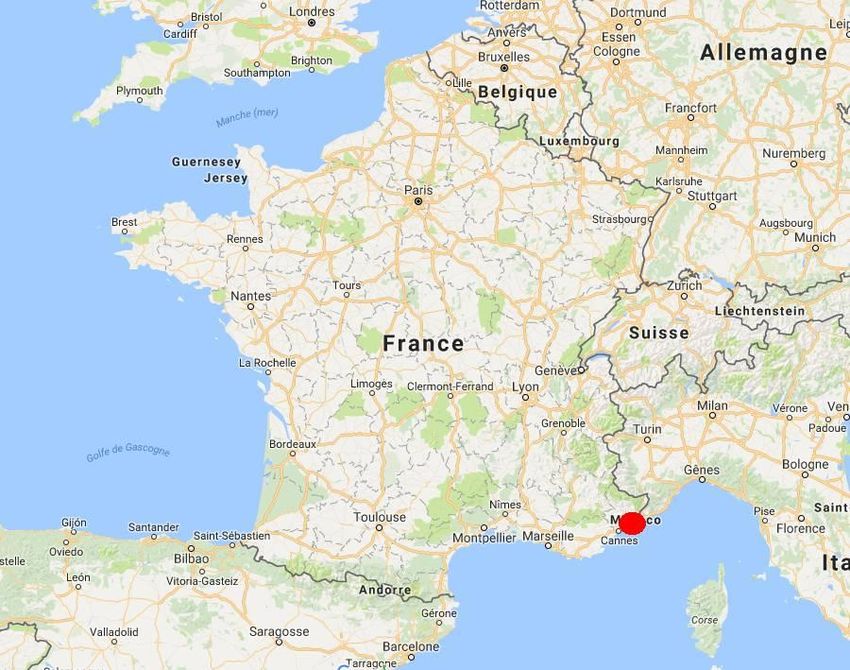
Pulse Summer School, Epitaxy Bases & Promises, Porquerolles, 2-8 July 2021 17Moore’s Law
Moore’s Law:
“Doubling in the
number of
components per
integrated circuit
(every 1.5 to 2-years)”
Gordon Moore (1965)
Reduction of the size
of the MOSFET
Pulse Summer School, Epitaxy Bases & Promises, Porquerolles, 2-8 July 2021 18Moore’s Law
Reduction of the size
of the MOSFET
The fabrication cost is divided by 10 every ~5 years
Pulse Summer School, Epitaxy Bases & Promises, Porquerolles, 2-8 July 2021 19Transistor dimensions & performances
Following the scaling rules has a strong impact
on the MOSFET performances
Vdd : operating
voltage
Vth (VT): threshold
voltage
tox : oxide
thickness
Increase of the maximum operating frequency
Pulse Summer School, Epitaxy Bases & Promises, Porquerolles, 2-8 July 2021 20Transistor dimensions & performances
Following the scaling rules has a strong impact
on the MOSFET performances
Shrinking of the silicon transistors presents multiple benefits:
Vdd : operating
voltage
Vth (VT): threshold
- a lower power
voltage consumption,
t-ox :increased
oxide performance (i.e. faster transistors operating at higher frequencies)
thickness
- increasing functionality (primary by increasing the transistor density)
- a reduction in the fabrication cost per transistor…
Pulse Summer School, Epitaxy Bases & Promises, Porquerolles, 2-8 July 2021 21Transistor dimensions & performances
Following the scaling rules has a strong impact
on the MOSFET performances
Proper scaling of MOSFET requires:
Vdd : operating
voltage
- a size reduction of the gate length and width but NOT only
Vth (VT): threshold
--> voltage
it requires a reduction of all other dimensions
tox : oxide
-thickness
including the gate/source and gate/drain alignment,
- the oxide thickness and the depletion layer widths,
- scaling of the substrate doping density…
Pulse Summer School, Epitaxy Bases & Promises, Porquerolles, 2-8 July 2021 22Scaling rules
If a CMOS technology generation has:
- a minimum channel length and width (L & W),
- an oxide thickness tox,
- a substrate doping NA,
- a power supply voltage VDD,
- a threshold voltage Vth, etc.
Downscaling of the gate length and
width, oxide thickness, junction
depth, and substrate doping.
Supply and threshold voltages are
also scaled by a factor of γ.
The electric field is constant
(rules developped by
Robert Dennard in 1974).
The transistor density is increased
by factor of γ2.
Pulse Summer School, Epitaxy Bases & Promises, Porquerolles, 2-8 July 2021 23Scaling rules
Two types of scaling (S = 1/0.7) can be used:
1) constant voltage scaling
Avoid the previous problem = preferred scaling method
since it provides voltage compatibility with older circuit
technologies.
The disadvantage of constant voltage scaling
is that the electric field increases as the
minimum feature length is reduced. This
leads to velocity saturation, mobility
degradation, increased leakage currents and
lower breakdown voltages.
Pulse Summer School, Epitaxy Bases & Promises, Porquerolles, 2-8 July 2021 24Scaling rules
Two types of scaling (S = 1/0.7) can be used:
2) constant field scaling
requires a reduction in Vdd as one decreases the
minimum feature size.
Difficulty of lowering Vth
(VGS)
Limit of MOSFET operation (VGS)
with a minimum overdrive
voltage (VDD – Vth)
Trade-off between
performance & high-density
leakage power dissipation (µm) [Trans. Electr. Electron. Mater. 11(3) 93 (2010): Y.-B. Kim]
Pulse Summer School, Epitaxy Bases & Promises, Porquerolles, 2-8 July 2021 25Limit in the Reduction of the transistor size
Evolution of the MOSFET transistor
channel since 1970
Technology node (Lgate)
As of 1980, the size reduction
has been exponential
Scaling to keep up with the demand
for faster, smaller, cheaper products
without any significant changes,
relying on improved lithography processes
(used to transfer the electronics network
patterns to every layer of IC)
Pulse Summer School, Epitaxy Bases & Promises, Porquerolles, 2-8 July 2021 26Limit in the Reduction of the transistor size
Evolution of the MOSFET transistor
channel since 1970
Technology node (Lgate)
As of 1980, the size reduction
has been exponential
Scaling to keep up with the demand
for faster, smaller, cheaper products
without any significant changes,
relying on improved lithography processes
(used to transfer the electronics network
patterns to every layer of IC)
As the technology node reached
90 nm (in 2005), challenges started to
appear ! nano-electronic era
Pulse Summer School, Epitaxy Bases & Promises, Porquerolles, 2-8 July 2021 27Limit in the Reduction of the transistor size
Evolution of the MOSFET transistor
channel since 1970
Technology node (Lgate)
Increased
As of 1980, the leakage
size reduction currents,
has been exponential
Difficulty on increase of on-current,
Scaling to keep up with the demand
Large parameter variations (doping, Vth, etc.)
for faster, smaller, cheaper products
without any Low reliability
significant changes,and yield,
relying on improved lithography processes
Increase
(used to transfer in manufacturing
the electronics network cost, etc.
patterns to every layer of IC)
As the technology node reached
90 nm (in 2005), challenges started to
appear ! nano-electronic era
Pulse Summer School, Epitaxy Bases & Promises, Porquerolles, 2-8 July 2021 28Velocity Saturation & Mobility Degradation
The electron drift velocity in the channel is
proportional to the electric field @ low
electric field values.
It starts to saturate at high E.
velocity saturation (Vsat). V = µE
For short channel devices, the longitudinal
electric field increases. At high E, the
velocity saturation affects the I-V
characteristics of the MOSFET.
For the same VGS (gate voltage), the saturation
mode is reached at smaller values of VDS and
leads to saturation current reductions.
Due to higher vertical electric fields, the
carriers of the channel scatter off of the oxide
interface.
This results in the degradation of carrier
mobility and the reduction in drain current.
[R. Trew, « High-Frequency Solid-State Electronic Devices »,
IEEE Pulse
Trans. on Elec. Devices(2005),
Summer 10.1109/TED.2005.845862]
School, Epitaxy Bases & Promises, Porquerolles, 2-8 July 2021 29Velocity Saturation & Mobility Degradation
The electron drift velocity in the channel is
proportional to the electric field @ low
electric field values.
It starts to saturate at high E.
velocity saturation (Vsat).
Both saturation field & the saturation velocity
For short channelof a semiconductor
devices, the longitudinal material are typically
electric field increases. At high E, the
strong function of:
velocity saturation affects I-V
characteristics -ofimpurities,
the MOSFET.
For the same VGS- (gate voltage),
crystal the saturation
defects,
mode is achieved at smaller values of drain-
- operating
source voltage and temperature.
saturation current reductions.
Due to higher vertical electric fields, the
carriers of the channel scatter off of the oxide
interface.
This results in the degradation of carrier
mobility and the reduction in drain current.
Pulse Summer School, Epitaxy Bases & Promises, Porquerolles, 2-8 July 2021 30IRDS nodes from 2020 to 2034
IRDS (Int. Roadmap for Devices and Systems) 2020
Modification/improvement of the device design
Pulse Summer School, Epitaxy Bases & Promises, Porquerolles, 2-8 July 2021 31FinFET Technology
A fin field-effect transistor is a multi-gate device MOSFET built on a substrate where the gate is
placed on 2, 3, or 4 sides of the channel or wrapped
around the channel, forming a double or even multi gate FET
--> technology started to be implemented in 2011
Excessive reduction of the gate length (LG) in conventional
MOSFET leads to an increase of the leakage current
--> excessive stand-by power consumption.
FinFET has improved electrostatics enabling the further
scaling of LG and contact gate/poly pitch (CPP).
[K. Cheng et al., ECS Transactions 80, 17 (2017)]
Reduction of Vth
active power
consumption
(reduction of VDD)
performances
(@cst Pconsumption)
Pulse Summer School, Epitaxy Bases & Promises, Porquerolles, 2-8 July 2021 32Improvement of the Performances
ITRS (Int. Tech. Roadmap for Semicond.) 2010
Heterogeneous integration
High mobility materials
(SiGe, III-V)
introduction on a Si platform
and a multi-gate based
technology
--> Compatibility with the
FinFET-based technology
Pulse Summer School, Epitaxy Bases & Promises, Porquerolles, 2-8 July 2021 33IRDS nodes from 2020 to 2034
IRDS (Int. Roadmap for Devices and Systems) 2020
Modification/improvement of the channel structure
Pulse Summer School, Epitaxy Bases & Promises, Porquerolles, 2-8 July 2021 34Heterogeneous Integration
Wednesday, July 7th 2021
Porquerolles, France 35Heterogeneous Material Integration on Si Platforms
Growing need to integrate more functionality into a smaller form factor with
power-performance benefits
Need for disruptive solutions to solve Si CMOS scaling limitations
new on-chip functionalities (sensors, optoelectronics, power management, RF… )
Complex electronic system are still fabricated using a wide range (mix) of technologies
(combining chips of last generation CMOS with older process technology chips in RF, MEMS…)
Integration of heterogeneous components for performance, power & cost improvement
Beyond multichip modules & system in package
on-chip integration
Co-integration at the material level
(in a compact volume)
High Mobility Materials for CMOS Applications.
https://doi.org/10.1016/B978-0-08-102061-6.00001-X
© 2018 Elsevier Ltd. All rights reserved.
Pulse Summer School, Epitaxy Bases & Promises, Porquerolles, 2-8 July 2021 36Heterogeneous Material Integration on Si Platforms
Growing need to integrate more functionality into a smaller form factor with
power-performance benefits
Need for disruptive solutions to solve Si CMOS scaling limitations
new on-chip functionalities (sensors, high-speed I/O, optoelectronics, power management, and RF)
Compatibility with large-scale 300 mm CMOS processes
Complex electronic system are still fabricated using a wide range (mix) of technologies
Epitaxial techniques/processes adapted to:
(Mixed-signal integrated circuit - e.g. in telecommunications)
- Defect
Pressure to integrate heterogeneous components for performance, power and cost
- Stress
improvement management
Beyond
- Thermal multichip modules & system in package
budget
on-chip & on-die integration
Co-integration at the material level
High Mobility Materials for CMOS Applications.
https://doi.org/10.1016/B978-0-08-102061-6.00001-X
© 2018 Elsevier Ltd. All rights reserved.
Pulse Summer School, Epitaxy Bases & Promises, Porquerolles, 2-8 July 2021 37Heterogeneous Material Integration on Si Platforms
Integrate (onto Si) heterogeneous devices with CMOS transistors
introduction of materials with specific properties
Semiconductor materials chosen for
their specific properties (Eg, µ)
e.g. InP, InGaAs, GaAs and GaN
developed for mixed-signal
analog RF applications
Pulse Summer School, Epitaxy Bases & Promises, Porquerolles, 2-8 July 2021 38Heterogeneous Material Integration on Si Platforms
Integrate (onto Si) heterogeneous devices with CMOS transistors
introduction of materials with specific properties
Semiconductor materials chosen for
their specific properties (Eg, µ)
e.g. InP, InGaAs, GaAs and GaN
developed for mixed-signal
analog RF applications
Replacement of the Si channel of the MOSFET
- Use of strained Si
- Use of SiGe technology characterized by
a higher mobility
- Use of a III-V material
Pulse Summer School, Epitaxy Bases & Promises, Porquerolles, 2-8 July 2021 39High Electron Mobility Transistor
A high-electron-mobility transistor (HEMT) is a FET incorporating a heterojunction between
two materials with different band gaps as the channel instead of a doped region (as is
generally the case for a MOSFET).
HEMTs are used in integrated circuits as digital on-off switches & as amplifiers.
They are able to operate at higher frequencies than ordinary transistors, up to millimeter wave
frequencies.
Applications: high-frequency products such as cell phones, satellite television receivers, voltage
converters, and radar equipment. They are widely used in satellite receivers, in low power amplifiers
and in the defense industry.
https://en.wikipedia.org/wiki/High-electron-mobility_transistor
Pulse Summer School, Epitaxy Bases & Promises, Porquerolles, 2-8 July 2021 40High Electron Mobility Transistor
The HEMT high carrier mobility and switching speed come from his specific design:
The wide band element (barrier) is typically doped with donor atoms
and has excess electrons in its conduction band.
The e- diffuse to the adjacent narrow band material CB
due to the availability of states with lower energy.
The movement of electrons will cause a change in
potential and thus an electric field between the
materials.
The electric field will push electrons back to the wide band
element CB. The diffusion process continues until electron
diffusion and electron drift balance each other, creating a
junction at equilibrium similar to a p-n junction.
The undoped narrow band gap material now has excess
majority charge carriers --> 2DEG
The fact that the charge carriers are majority carriers yields Supriya, Sweety. (2012).
high switching speeds, and the fact that the low band gap Ballistic Mobility Degradation Effect
semiconductor is undoped means that there are no donor in 25 nm Single Gate HEMT.
atoms to cause scattering and thus yields high mobility.
Pulse Summer School, Epitaxy Bases & Promises, Porquerolles, 2-8 July 2021 41Band Structure Engineering
Heteroepitaxy band structure design
& engineering for high performance devices
Combining different III-V materials leads
to a large variety of band structures
(band alignments)
Fabrication of complex heterostructures
In lattice-matched systems:
- Si, GaP, AlP AlAs
- Ge, GaAs, AlAs
Using III-V alloys:
- (In,Ga,Al)As
- (In,Ga,Al)P
- (In,Al,Ga)N
Pulse Summer School, Epitaxy Bases & Promises, Porquerolles, 2-8 July 2021 42Band Structure Engineering
Heteroepitaxy band structure design
& engineering for high performance devices
Epitaxial stress:
e = (asub. – alay.) / alay.
e < 0: compressive stress
e > 0: tensile stress
Critical thickness
(pseudomorphic growth)
hc 1 / ε
For h > hc : strain relaxation
(creation of defects)
Chapter 3 – Monolithic Integration of InGaAs on Si(001) Substrate for Logic Devices , Clément Merckling
High Mobility Materials for CMOS Applications. https://doi.org/10.1016/B978-0-08-102061-6.00004-5
Pulse Summer School, Epitaxy Bases & Promises, Porquerolles, 2-8 July 2021 43Epitaxy Defect Engineering
Wednesday, July 7th 2021
Porquerolles, France 44Heterogeneous Material Integration on Si Platforms
Key challenge --> elimination of the
dislocations formed when Ge or III-V
materials are grown on Si.
A variety of techniques includes:
- compositional grading,
- wafer bonding,
- selective area growth,
- aspect ratio trapping,
- cyclic annealing. [D. Caimi et al.,
Solid-State Electronics
185, 108077 (2021)]
Patterned selective-area-growth (SAG) methods provide a direct and potentially more
flexible means to directly integrate disparate materials if defectivity can be managed.
Selective area epitaxy is a local growth through a patterned amorphous dielectric mask
(typically SiO2 or Si3N4) deposited on a semiconductor substrate. Semiconductor growth conditions
are selected to ensure epitaxial growth on the exposed substrate, but not on the dielectric mask.
Pulse Summer School, Epitaxy Bases & Promises, Porquerolles, 2-8 July 2021 45Heterogeneous Material Integration on Si Platforms
Key challenge --> elimination of the
dislocations formed when Ge or III-V
materials are grown on Si.
A variety of techniques includes:
- compositional grading,
- wafer bonding,
- selective area growth,
- aspect ratio trapping,
- cyclic annealing.
Patterned selective-area-growth (SAG) methods provide a direct and potentially more flexible
means to directly integrate disparate materials if defectivity can be managed.
Selective area epitaxy is a local growth through a patterned amorphous dielectric mask (typically
SiO2 or Si3N4) deposited on a semiconductor substrate. Semiconductor growth conditions are
selected to ensure epitaxial growth on the exposed substrate, but not on the dielectric mask.
Pulse Summer School, Epitaxy Bases & Promises, Porquerolles, 2-8 July 2021 46Selective Area Growth
Selective area growth (SAG) --> local growth of an epitaxial layer on a substrate through
a patterned dielectric mask (typically silicon oxide (SiO2) or silicon nitride (Si3N4)).
10 – 500 nm thick, covering a part of the substrate surface & leaving a defined Si
surface – the “active area” – exposed for the growth of the active layers.
Objective: to promote the growth of the layer only [N. Collaert et al., Microelec.Eng.132 (2015) 218]
in the active area w/o nucleation on the mask
exclusively in a lithography defined area, this
process enables alignment for the later device
fabrication. But the growth condition windows are
reduced to favour the growth rate locally
depending on the mask dimensions &
the dielectric layer nature.
Crystalline quality, process selectivity,
thickness, doping control, faceting need to be
investigated.
Pulse Summer School, Epitaxy Bases & Promises, Porquerolles, 2-8 July 2021 47Aspect Ratio Trapping
ART has been developed to integrate Ge or III-V devices with CMOS: the buffer layer is
thin (< 1 μm) to allow a standard CMOS back-end process, the technique has a low thermal
budget, and the process can be applied to large wafers to allow integration into a CMOS process.
Ge or III-V material is epitaxially grown in
high aspect ratio holes or trenches formed
in dielectric layers on silicon.
In ART, dislocations are guided to the
dielectric sidewalls
and trapped, producing a
low-dislocation density
region at the top of the trench.
Typically, the trenches are formed in
thermally-grown SiO2 by lithography &
RIE etching (in the fig., they are
800 nm deep, 200 nm wide and millimeters long). [J. G. Fiorenza et al., ECS Transactions, 33 (6) 963-976 (2010)]
Pulse Summer School, Epitaxy Bases & Promises, Porquerolles, 2-8 July 2021 48Aspect Ratio Trapping
The threading dislocations originating from the III-V/Si hetero-interface are guided to
the oxide sidewalls, resulting in dislocation-free regions above a critical thickness.
The “trapping” of threading segments in the ART technique is attributed to the crystallographic
geometry: in the {111}/ cubic slip system, misfit dislocations lie along the ⟨110⟩ directions
in the (100) growth plane, while the threading segments rise up on the {111} planes in the ⟨110⟩
directions.
[Qiang Li et al., Progress in Crystal Growth &
Characterization of Materials 63 (2017) 105–120]
Pulse Summer School, Epitaxy Bases & Promises, Porquerolles, 2-8 July 2021 49Aspect Ratio Trapping
ART has been developed to integrate Ge or III-V devices with CMOS: the buffer layer is
thin (< 1 μm) to allow a standard CMOS back-end process, the technique has a low
thermal budget, and the process can be applied to large wafers to allow integration into
a state-of-the-art CMOS process.
Ge or III-V material is epitaxially grown in
high aspect ratio holes or trenches formed
in dielectric layers on silicon.
In the ART technique, dislocations
are guided to the dielectric sidewalls
and trapped, producing a
low-dislocation density
region at the top of the trench.
Typically, the trenches are formed in
thermally-grown SiO2 by lithography &
RIE etching (in the fig., they are
800 nm deep, 200 nm wide and millimeters long). [J. G. Fiorenza et al., ECS Transactions, 33 (6) 963-976 (2010)]
The TEM images demonstrate that the threading dislocations are eliminated in
the top of the trench for a large total area of material (~5 µm2)
Pulse Summer School, Epitaxy Bases & Promises, Porquerolles, 2-8 July 2021 50Aspect Ratio Trapping
ART is effective in reducing the surface TDD
The surface dislocation density is reduced
by 3 orders of magnitude from blanket Ge on Si.
The TDD decreases proportionately with the aspect
ratio (trench height/trench width)
the aspect ratio itself plays an important role
in the mechanism by which ART reduces the TDD
ART is applicable to a variety of III-V
materials (GaAs, InP).
[J. G. Fiorenza et al., ECS Transactions, 33 (6) 963-976 (2010)]
Pulse Summer School, Epitaxy Bases & Promises, Porquerolles, 2-8 July 2021 51Aspect Ratio Trapping
Important reduction of the dislocation density within a thin deposited layer thickness
(few hundreds of nm)
The key challenge of this technique resides in the impossibility to trap the (111)-
oriented defects along the parallel direction of the trench.
[C. Merckling et al.,
ECS Transactions 66, 107 (2015)]
Pulse Summer School, Epitaxy Bases & Promises, Porquerolles, 2-8 July 2021 52Challenges in III-V/Si Hetero-Epitaxy
A specific defect is antiphase-domains (APD) due to the lack of inversion symmetry of
III-V materials --> the sub-lattices are occupied by different atom species.
The bonds are polar due to the difference in the ionicity of the constituent atoms.
APDs are inherent to polar-on-non-polar growth. Single layer steps produce 2
domains in the III-V overlayer whereas double-layer steps do not.
[Qiang Li et al., Progress in Crystal Growth &
Characterization of Materials 63 (2017) 105–120]
Pulse Summer School, Epitaxy Bases & Promises, Porquerolles, 2-8 July 2021 53Challenges in III-V/Si Hetero-Epitaxy
Development of surface preparation processes
Importance of the III-V/Si surface engineering to control the APD generation
Promotion of double-layer steps at the surface
Si (001) substrate (with a 0.15° misorientation in the [110] direction) is deoxidized in using NF3/NH3
remote plasma and then annealed (1 min–10 min) in an MOCVD reactor at high temperature
(800 °C–950 °C) in H2 ambient.
formation of double steps and growth of GaAs
[R. Alcotte et al., APL Mater. 4 (4) (2016) 046101]
Pulse Summer School, Epitaxy Bases & Promises, Porquerolles, 2-8 July 2021 54Aspect Ratio Trapping Patterned Si
The use of {111} Si V-grooves in the ART growth process has been developped.
The crystallographic alignment between the Si and III-V materials in the V-grooves avoids
the introduction of APDs.
Crystallography analysis indicates that III-V SC on the two {111} facets of the “V-
shape” have the same polarity. In principle, the Si (111) surface can also have surface steps, as
in the case of Si (001) --> A single step on the Si (111) surface has the height of one
Si (001) double-layer (0.31 nm). Such steps will not lead to the formation of APBs.
III-V nucleation on Si (111) generates less defects as compared to nucleation on Si (001)
& avoid the formation of the (111)-oriented defects along the parallel direction of the
trench.
A III-V lattice in the V-shape of Si with
{111} facets along the [110] direction.
[Qiang Li et al., Progress in Crystal Growth &
Characterization of Materials 63 (2017) 105–120]
Pulse Summer School, Epitaxy Bases & Promises, Porquerolles, 2-8 July 2021 55SiGe & III-V technology
Wednesday, July 7th 2021
Porquerolles, France 56Beyond the Si Channel
Replacement of the Si channel in MOSFET with higher mobility (or injection velocity)
materials.
Research efforts have focused on improving the effective mass (m*)
- strained Si MOSFET technology
Beyond the traditional silicon channel materials:
- Ge-based materials for improving PMOS (low hole mass m*)
- III-V-based materials for improving NMOS (low electron mass m*)
µ 1 / m*
Pulse Summer School, Epitaxy Bases & Promises, Porquerolles, 2-8 July 2021 57Strained Si MOSFET Technology
Strained Si channels have been introduced since the 90 nm node technology
Use of epitaxial processes involving MOCVD or MBE growth
higher speed operation ( µ) & improved current-voltage performances
The carrier mobility increase, implemented by appropriate Si strain, provides higher speed of the
carriers under the same conditions of polarization and a fixed oxide thickness.
Or with the same current conditions in the channel, thicker oxides and/or lower voltage supply
can be used relaxation of compromise between current, consumption
& short channel effects
Ge has a lattice constant of 5.658 Å with Si (5.431 Å) up to 4.2% lattice-mismatch
Use of an SiGe « template » to biaxially strain Si
--> The tensile stress causes an increase in
the lattice parameter of strained silicon
[Dismukes, J.P. et al.,
JAP 35 ,1964, 2899]
Pulse Summer School, Epitaxy Bases & Promises, Porquerolles, 2-8 July 2021 58Strained Si MOSFET Technology
IEEE TRANS. ON ELECTRON DEVICES, 47, 1406, JULY 2000
The strain leads to an energy splitting of the Si
conduction band edge.
It lifts the six fold degeneracy in the conduction band and
lowers the two perpendicular valleys (labeled D2) with respect
to the four in-plane valleys.
Electrons are expected to preferentially occupy the
lower-energy valleys, reducing the effective in-plane
transport mass.
The energy splitting also suppresses intervalley
phonon-carrier scattering, increasing the electron low-
field mobility.
Pulse Summer School, Epitaxy Bases & Promises, Porquerolles, 2-8 July 2021 59Strained Si MOSFET Technology: Electron Transport
IEEE TRANSACTIONS ON ELECTRON DEVICES, VOL. 47, p. 1406, JULY 2000
The strain leads to an energy splitting of the Si
conduction band edge.
ELECTRONICS, VOL. 18,
It lifts the six fold degeneracy in the conduction band and NO. 2, p. 63 (2014)
lowers the two perpendicular valleys (labeled D2) with respect
to the four in-plane valleys.
Electrons are expected to preferentially occupy the
lower-energy valleys, reducing the effective in-plane
transport mass.
The energy splitting also suppresses intervalley
phonon-carrier scattering, increasing the electron low-
field mobility.
Pulse Summer School, Epitaxy Bases & Promises, Porquerolles, 2-8 July 2021 60SiGe channels
Utilization of strained materials such as strained Si for n-FET and strained SiGe for p-FET are
developped as a near-term technological solution.
SiGe layers pseudomorphically grown on Si substrates are under biaxial compressive
strain. SiGe layers on relaxed SiGe underlying buffers can have either biaxial compressive
or tensile strain depending on the relative lattice mismatch between the two layers.
Strain plays a role on the band structure and transport properties of SiGe channels
For y > x, the buried Si1-yGey layer is under
biaxial compressive strain.
The strained-Si1-yGey layer is capped with Si for surface
passivation to control the interface traps for SiGe.
The band alignment of strained Si and strained
SiGe mostly confines the holes in the buried SiGe &
the electrons in the strained-Si capping layer.
Chapter 6 – SiGe Devices, Pouya Hashemi and Takashi Ando
High Mobility Materials for CMOS Applications.
https://doi.org/10.1016/B978-0-08-102061-6.00004-5
Pulse Summer School, Epitaxy Bases & Promises, Porquerolles, 2-8 July 2021 61SiGe channels: Hole Transport
Hole mobility monotonically increases with increasing Ge content in the biaxially strained-
SiGe. Adjusting the Ge content in the channel and the buffer, a wide range of mobility values can be
achieved mobility enhancements up to 10x over (100)-Si.
Moreover, extremely high hole effective mobility numbers > above 1000cm2/V.s have
been measured for buried-channel strained-Si1-yGey quantum wells.
Strained Si
Strained Si1-yGey
Relaxed Si1-xGex
The effective mass of SiGe is a strong
function of Ge fraction, strain state
(compression or tension), and strain type
(uniaxial, biaxial).
Pulse Summer School, Epitaxy Bases & Promises, Porquerolles, 2-8 July 2021 62SiGe channels: Hole Transport
The biaxial strain is shown to lift the degeneracy of the heavy-hole and light-hole subbands in the
valence band, in addition to the effective mass reduction.
On the other hand, the theory suggests that the uniaxial compressive strain can further
reduce the hole effective mass and is the optimum strain for the hole transport. The
calculated hole effective mass of relaxed and uniaxially strained SiGe, lattice matched to Si, for
various Ge fractions and surface orientations.
The hole effective mass decreases with
increasing Ge content and uniaxial strain.
A way to achieve uniaxial strain is to start
from globally biaxial strained substrates and
pattern them to high-aspect-ratio fingers or
bars leading to strain relaxation along one
direction.
Pulse Summer School, Epitaxy Bases & Promises, Porquerolles, 2-8 July 2021 36Integration of devices on a Si CMOS platform
Demonstration of a GaAs MOSFET on silicon using ART.
The transfer characteristics showed a peak mobility of 503 cm2/Vs, which was
similar to the value seen on a GaAs MOSFET made on a bulk GaAs substrate using the
same MOSFET fabrication process, and which exceeds the silicon universal mobility
curve.
[Y. Q. Wu et al., Appl. Phys. Lett. 93,
242106 (2008)]
Pulse Summer School, Epitaxy Bases & Promises, Porquerolles, 2-8 July 2021 64InGaAs-based channel FinFET
Initiation of the growth on the Si {111} planes and use of an InP buffer layer.
Steps of chemical mechanical polishing (CMP) / chemical etching for InP recess.
Growth of the In0.53Ga0.47As channel layer --> the depth of the InP recess determines
the thickness/height of the InGaAs channel. [N. Waldron et al., Solid-State Electronics 115, 81 (2016)]
The STI oxide is recessed and then follows a typical Si Fin.
Pulse Summer School, Epitaxy Bases & Promises, Porquerolles, 2-8 July 2021 65GaN Electronics
Wednesday, July 7th 2021
Porquerolles, France 66Why GaN ?
Optoelectronic Applications: UVC
UVB
UVA
LED, lasers, …
Wide band Gap semiconductors
(AlN, GaN)
From IR to UV
Wide range of applications
White light
LED
“ For the invention of efficient blue LEDs which has
enabled bright and energy-saving white light
sources “
Pulse Summer School, Epitaxy Bases & Promises, Porquerolles, 2-8 July 2021 67Why GaN ?
Electronic Components:
Telecommunication, radars, power electronics,…
Properties (300 K) Si InP GaAs 4H-SiC GaN
Band Gap Energy (eV) 1.12 1.35 1.43 3.25 3.43
Breakdown Field Fcl (MV/cm) 0.3 0.45 0.4 3 3 Pmax I max Vcl
Electron Saturation Velocity
vs (x107 cm/s)
1.1 1 1 2 1.8 f c vsat
Thermal Conductivity (Cut-off frequency)
ΘK (W/cm.K)
1.5 0.7 0.5 4.9 1.5
GaN --> high breakdown field, good thermal conductivity, high electron saturation velocity
Pulse Summer School, Epitaxy Bases & Promises, Porquerolles, 2-8 July 2021 68Why GaN ?
Electronic Components:
Heterostructure
Heterostructure
→ 2D electron gas
→ 2D electron gas
Telecommunication, radars, power electronics,…
GaAs
GaN: well-adapted materialfor high-frequency high-power electronic components
Pulse Summer School, Epitaxy Bases & Promises, Porquerolles, 2-8 July 2021 69New players
Optoelectronic Applications:
have entered the
market with
GaN-on-Si
enhancement-mode
(E-mode)
high-electron-
mobility LED, lasers, …
Transistor
(HEMT)Properties
technology
(300 K) Si InP GaAs 4H-SiC GaN
Band Gap Energy (eV) 1.12 1.35 1.43 3.25 3.43
Breakdown Field Fcl (MV/cm) 0.3 0.45 0.4 3 3
Electron Saturation Velocity
1.1 1 1 2 1.8
vs (x107 cm/s)
Thermal Conductivity
www.semiconductor-today.com/ 1.5 0.7 0.5 4.9 1.5
ΘK (W/cm.K)
news_items/2021/may/
yole-100521.shtml
GaN: strong candidate for high-frequency high-power electronic components
Pulse Summer School, Epitaxy Bases & Promises, Porquerolles, 2-8 July 2021 70GaN Crystal Structure & Polarization N
Wurtzite structure with two hexagonal sublattices Ga
A unique c-polar axis c
Non ideal wurtzite structure
u
the tetrahedron is distorted
c shorter = tetrahedron compressed along c
a
Spontaneous polarization (Psp)
Ideal wurtzite
The direction depends on
the film polarity c/a c/u
(Ga or N polar)
1.633 2.666
PSp PSp
AlGaN GaN
(Ga, Al) polar
Pulse Summer School, Epitaxy Bases & Promises, Porquerolles, 2-8 July 2021 71Polarization in Heterostructures
Wurtzite structure with two hexagonal sub-lattices
UVC
A unique c-polar axis UVB
UVA
Piezoelectric polarization (Ppz )
Due to the epitaxial strain
(the direction depends on the type of strain) Tensile strain Compressive strain
PSp PPz PSp PPz
Total polarization (P = Psp + Ppz)
AlGaN GaN
c
PSp PSp
GaN AlGaN
Pulse Summer School, Epitaxy Bases & Promises, Porquerolles, 2-8 July 2021 72Polarization in a AlGaN/GaN Heterostructure
Total polarization (P = Psp +Ppz) Tensile strain
Heterostructure -spol bar
PSp PPz
AlGaN
Different total polarization AlGaN barrier +spol bar barrier
c -spol channel
Charge densities at the interface PSp GaN
GaN channel +spol channel channel
Internal electric field
Conduction Growth direction
F = DP= (Pbar-Pcha)/ee0 = s/ee0 band
Band structure bending Undoped
Fermi GaN
HEMT heterostructure: level AlGaN
A cladding barrier (larger gap than GaN)
is grown on the GaN channel
2DEG
At the AlGaN/GaN interface: polarization
formation of a triangular QW
difference and conduction band discontinuity 2D electron gaz (2DEG)
Electron density N = s / q
Pulse Summer School, Epitaxy Bases & Promises, Porquerolles, 2-8 July 2021 73Comparison of Si, GaAs and GaN
Comparison of the main properties for power and microwave applications
temperature
breakdown frequency
noise
current
https://sudonull.com/post/29796-Why-silicon-and-why-CMOS
Pulse Summer School, Epitaxy Bases & Promises, Porquerolles, 2-8 July 2021 74Hetero-Epitaxial Growth of GaN on Si
Lack of GaN native substrates:
- limited supply & very expensive (few thousand $)
Growth on Si (less than 100 $ for 200 mm wafer)
--> large lattice-mismatch & thermal mismatch
Pulse Summer School, Epitaxy Bases & Promises, Porquerolles, 2-8 July 2021 75Hetero-Epitaxial Growth of GaN on Si
Main difficulties:
- the “melt-back etching” --> reaction between Ga & Si at high temperature
If Ga comes into contact with Si
during growth, this leads to
melt-back etching which generates
large defects in the GaN structures.
Use of a blocking layer between
GaN and Si --> AlN
GaN
AlN
Chapter 4 – III-N Epitaxy on Si for Power Electronics
Si substrate M. Charles, Y. Baines, E. Morvan and A. Torres
High Mobility Materials for CMOS Applications.
https://doi.org/10.1016/B978-0-08-102061-6.00004-5
Pulse Summer School, Epitaxy Bases & Promises, Porquerolles, 2-8 July 2021 76AlN Buffer Layer on Si by MBE rms = 0.32 nm
Nucleation process to obtain a sharp AlN/Si interface
RHEED patterns along the [–110] azimuth of
Si(111) during AlN nucleation using a NH3-first
nucleation process.
(a) after NH3 pre-flow of Si(111) at 650°C and in-situ 1200°C 500 nm
rapid thermal annealing at 820°C, a (8 × 8) surface
reconstruction characteristic of β -Si3N4 (0001)
surface is obtained. rms = 0.24 nm
(b) After deposition of 1 monolayer of Al at 650°C,
the AlN(0001) (1 × 1) orders indicated by white arrows
coexist with the Si(111) ones.
(c) after the growth of 40 nm AlN buffer layer at 920°C.
500 nm
F. Semond , MRS BULLETIN AFM
VOLUME 40, MAY 2015
DOI: 10.1557/mrs.2015.96
TEM Porquerolles, 2-8 July 2021
Pulse Summer School, Epitaxy Bases & Promises, 77Hetero-Epitaxial Growth of GaN on Si
Main difficulties:
- the melt-back etching --> reaction between Ga & Si at high temperature
- high dislocation density --> lattice-mismatch aGaN = 0.318 nm, a = 5.59x10⁻⁶ K-1
- large stress --> thermal expansion coef. mismatch aSi(111) = 0.384 nm, a = 3.59x10⁻⁶ K-1
lattice-mismatch = 16.9%
TEC mismatch = 56%
Integration of GaN on silicon --> « manufacturability »
(compatibility of the wafers with a standard Si production line)
Low bow, low particule/defect count of the wafers & crack-free surface
Cracking of a GaN/Si structure due to the large
tensile stress during the cooling process from
growth temperature to room temperature
originating from the TEC mismatch
Pulse Summer School, Epitaxy Bases & Promises, Porquerolles, 2-8 July 2021 78Design of the Heterostructure
Integration of layers to control the strain:
To grow crack-free GaN layers on Si, it is necessary to maintain a certain amount of
compressive strain in GaN in order to compensate for the tensile strain appearing during the post
growth cooling from the growth temperature to room temperature.
Growth under compressive
strain --> low Al content
Layers on high Al content
ones
to prevent cracking, growth
of GaN must be 2D, which
also means that the surface
morphology of the initial
AlN or AlGaN buffer layer
needs to be as smooth as
possible.
Pulse Summer School, Epitaxy Bases & Promises, Porquerolles, 2-8 July 2021 79Design of the Heterostructure
Designing structures to preserve a compressive strain:
1. Graded aluminum from AlN to GaN: with a smooth
grading or a step grading of different AlxGa1-xN layers
to continually introduce compression into the layers.
2. AlN interlayers: after growing GaN on the Al(Ga)N
nucleation layer, a new AlN layer is grown on this GaN layer. [B. Zhang et al., Chin. Sci. Bull. 1251 (2014)]
The AlN quickly reaches its critical strain thickness and then
relaxes. After, a GaN layer can be grown in compression
on the AlN layer.
Presence of a strain gradient during the growth of
the different layers (a slope of zero = fully relaxed structure)
Strong difference in the relaxation process between the first
& second GaN layer compressive strain of the structure
=
compensation of the tensile strain generated
during the cooling process
(In-situ curvature meas. gives the aver. deformation of the epitaxial structure)
Pulse Summer School, Epitaxy Bases & Promises, Porquerolles, 2-8 July 2021 80Design of the Heterostructure
Designing structures to preserve a compressive strain:
1. Graded aluminum from AlN to GaN: with either a smooth
grading or a step grading of different AlxGa1-xN layers in order to
continually introduce compression into the layers.
2. AlN interlayers: after growing GaN directly on the AlN
nucleation layer, a new AlN layer is subsequently grown on this GaN
layer. The AlN quickly reaches its critical strain thickness and then
relaxes. After this, a GaN layer can once again be grown in
compression on the AlN layer.
3. Thick superlattice structures: After the AlN nucleation layer,
successive pairs of AlN and GaN (or AlGaN) are grown, with the AlN
relaxing sufficiently to put the GaN in compression. The sum of the
tension in the AlN and compression in the GaN gives a net addition
of compression, and so, a large number of these repeats can
be used to create thick structures, before the addition of a
final GaN layer also in compression.
[B. Zhang et al., Chin. Sci. Bull. 1251 (2014)]
Pulse Summer School, Epitaxy Bases & Promises, Porquerolles, 2-8 July 2021 81Effect of the Barrier Material
Designing structures to improve the HEMT characteristics:
1. The AlGaN/AlN/GaN double heterojunction with the insertion
of a thin AlN layer of the order of 1nm between the AlGaN barrier and
the GaN channel. The AlN “spacer” layer
allows more e- to accumulate in the GaN channel spacer
combined with better confinement due to the
larger band offset which increases the mobility.
This gives lower sheet resistance: buffer layer
2. Design of the AlGaN capping with
larger Al content or lattice-matched AlInN
to reach larger Ns values.
Mobility μ > 1800 cm².V-1.s-1
Sheet carrier density > 1x1013 cm-2
@ 300K Schematic of a typical
[Y. Cordier et al., AlGaN/GaN HEMT structure
III-Nitride Semiconductors & [N. BARON, thèse, [S. RENNESSON, thèse,
their Modern Devices, 2013)] Univ. Nice (2009)] Univ. Nice (2013)]
Pulse Summer School, Epitaxy Bases & Promises, Porquerolles, 2-8 July 2021 82Combining MBE & MOCVD
AlGaN/GaN HEMTs on Si
One of the challenges is the vertical voltage-blocking capability of the GaN-on-Si epitaxial stack
which limits the maximum voltage operation.
Vertical buffer current is correlated to charge injection from the Si substrate
--> a parasitic channel forming between the AlN nucleation and the Si.
Suppression of the formation of this channel --> AlN growth temperature
Limit in MOCVD growth due to severe material quality degradation.
Hybrid growth approach
Combining the use of MBE AlN nucleation layer @ LT with a MOCVD HEMT structure.
Coll. CRHEA – Aachen Univ. & Magdeburg Univ.
[H. Yacoub et al., Phys. Status Solidi A, 1700638(2018)]
Pulse Summer School, Epitaxy Bases & Promises, Porquerolles, 2-8 July 2021 83Combining MBE & MOCVD
[H. Yacoub et al.,
Phys. Status Solidi A,
1700638(2018)]
C–V measurements on 150nm MBE AlN/p-Si test structures
@ 0V: hole accumulation is still observed and the capacitance decreases until 4V. No further
increase in Cp is observed at higher positive biases, indicating the suppression of e- accumulation
at the interface (an increase in the positive bias voltage regime initiated by carrier injection
originating from an inversion channel formed between AlN and the p-Si substrate). This e- channel is
responsible for the vertical leakage current in the buffer structure.
C–V profile shows no hysteresis (between to/back-sweeps): high AlN/Si interface quality.
Pulse Summer School, Epitaxy Bases & Promises, Porquerolles, 2-8 July 2021 84Combining MBE & MOCVD
Vertical buffer leakage (I–V): MOCVD-sample shows 1x10⁻⁴ Acm-2 current density @ 350V
& hybrid MBE/MOCVD-sample has the same J @ 445 V yielding an increase of 27%.
The hybrid growth reduces the vertical buffer current. The initial growth conditions
impact the voltage-blocking capabilities (@ 600 V 100x lower J for MBE/MOCVD structure).
Hall meas.: slight decrease in the channel mobility for MBE/MOCVD-sample. The mean
carrier concentrations are similar --> 2DEG properties of the samples are comparable.
Pulse Summer School, Epitaxy Bases & Promises, Porquerolles, 2-8 July 2021 85Perspectives & Challenges
Monolithic integration of III-V SC on Si attracts a lot of interest to benefit from the
superior electron mobility / high saturation velocity / high temperature / high power
Important improvements & achievements with demonstration of fully integrated III-V
devices on 300 mm Si substrates in a VLSI compatible flow [N. Waldron et al., Solid-State
Fin FET Electronics 115, 81 (2016)]
Gate All Around
direct optical band gap offers the Nanowires
possibility to integrate light sources on
Si for optical interconnections
Challenges still exist:
Control of the defects in
heteroepitaxy (lattice mismatch)
(III-V, IV-IV) in a compact volume,
compatible with Si CMOS devices.
In the longer term, new beyond-CMOS materials like CNTs and 2D materials may add
further to the material palette for heterogeneity and new nanosystems.
Pulse Summer School, Epitaxy Bases & Promises, Porquerolles, 2-8 July 2021 86Environmental Impact
Environmental footprint of
CMOS technologies
https://www.imec-int.com/en/articles/
environmental-footprint-logic-cmos-technologies
Pulse Summer School, Epitaxy Bases & Promises, Porquerolles, 2-8 July 2021 87Thank you for your attention
Wednesday, July 7th 2021
Porquerolles, France 88Transistor: Advantages & Challenges
Transistor Advantages Challenges
[K. Cheng et al., ECS Transactions 80, 17 (2017)]
Pulse Summer School, Epitaxy Bases & Promises, Porquerolles, 2-8 July 2021 89Issues for nanoscale MOSFET (1)
Reverse bias-pn junction leakage current
For heavily doped pn junction of drain/source and substrate regions, the band-to-
band tunneling (BTBT) effect dominates the reverse bias leakage current. In band-
to-band tunneling, electrons tunnel directly from the valence band of the p region
to the conduction band of the n region.
Subthrehold leakage current
When 0 < VGS < Vth : the transistor is biased in the subthreshold or weak inversion
region and the concentration of minority carriers is small but not zero.
Drain-Induced Barrier Lowering (DIBL)
Subthreshold leakage current is mainly due to drain-induced barrier lowering. In
short channel devices, the depletion region of drain and source interact with each
other and reduce the potential barrier at the source. The source is then able to
inject charge carriers into the surface of the channel resulting in subthreshold
leakage current (pronounced in high drain voltages and short channel devices).
Vth Roll Off
Vth reduces due to channel length reduction. The drain and source depletion
region enter further into the channel length, depleting a part of the channel.
Due to this, a lesser gate voltage is required to invert the channel reducing the
threshold voltage. The reduction in threshold voltages increases the subthreshold
leakage current as the subthreshold current is inversely proportional to the
threshold voltage.
Pulse Summer School, Epitaxy Bases & Promises, Porquerolles, 2-8 July 2021 90You can also read