Inverse designed arbitrary input and ultra compact 1 N power splitters based on high symmetric structure - Nature
←
→
Page content transcription
If your browser does not render page correctly, please read the page content below
www.nature.com/scientificreports
OPEN Inverse‑designed arbitrary‑input
and ultra‑compact 1 × N power
splitters based on high symmetric
structure
Hansi Ma1,2, Jie Huang2, Kaiwang Zhang1* & Junbo Yang2*
Based on high symmetric structure, we propose the arbitrary-input and ultra-compact 1 × 2 and 1 × 3
power splitters by utilizing inverse design method. These devices can realize the functionality of
power splitting, when the optical field is launched from arbitrary port. The shapes of their structures
are 3.8 μm-wide regular hexagon and 4.0 μm-wide regular octagon, respectively. By utilizing 3D
fine difference time domain solutions, the simulated results indicate that the excess loss of the
1 × 2 power splitter is less than 1.5 dB from 1,500 to 1,600 nm, and the excess loss and crosstalk of
the 1 × 3 power splitter are less than 1.9 dB and lower than − 15.5 dB over 100 nm bandwidth at the
centered wavelength of 1,550 nm respectively. In addition, the tolerances to fabrication errors are also
investigated.
As we all know, with the rapid development of photonics integrated circuits (PICs), more and more devices will be
put on the chip, such as mode division multiplexing (MDM)1–5, power splitter6–10, polarization beam splitter11–15
and optical m odulator16–18. In addition, current silicon-on-insulator (SOI) photonic circuits are constricted to a
single layer. If the key components completed their own functionality in multiple ports, the field of PICs might
allow for high device densities and complex photonic systems. For example, waveguide crossing can operate very
well when the light field is launched from output p ort19–23, and mode multiplexer can also be employed reversely
as mode demultiplexer in the MDM s ystems24–27. As one of the fundamental building elements for scaling
high-density PIC, power splitter has attracted substantial research interests. The authors fabricated, tested, and
compared 1 × 8 splitters formed by cascaded conventional b ranches28. A 1 × 16 optical power splitter with wide
splitting angle, uniform outputs, and low excess loss was d emonstrated29. But the footprint of the conventional
power splitters may be extremely large, which may impede their widespread applicability. In order to decrease
footprint, advanced inverse design methods were adopted to design power splitter. An ultra-compact colorless
50:50 coupler with the footprint of only 2.6 μm × 2.6 μm and a considerably smaller and more broadband 1 × 3
splitter with a design area of 3.8 µm × 2.5 µm were demonstrated30,31. These devices occupy both great perfor-
mances and compact footprints. Moreover, various power splitters with novel and practical characteristics have
been reported by means of computational optimization methods, including arbitrary-direction, multichannel
and ultra-compact power s plitters9, power splitter with arbitrary r atios32,33, the ultra-compact dual-mode and
three-mode 3-dB power splitters based on photonic crystal like s tructure34,35, and the novel 1 × 2 mode convert-
ers with multipurpose design goals which can simultaneously achieve power splitting and mode c onversion36.
Although power splitters become more pervasive, they can scarcely realize the functionality of power splitting by
launching the optical field from the output waveguide like waveguide crossing and mode multiplexer. Thus it can
be seen the design goals of being arbitrary-input and ultra-compact imposed on them become worth pursuing.
At the same time, an accumulating number of advanced optimization methods have been applied to design
complex nanophotonic devices, such as direct-binary-search (DBS) a lgorithm2,4,5,9,13,18,21,27,30,34,35, genetic
algorithm37,38, objective-first d
esign39–41, and fabrication-constrained nanophotonic inverse d esign42. Compared
with traditional approaches which strongly depend on analytic theory and intuition of researchers, the biggest
virtue of advanced optimization methods is that they can take full advantage of the available design space of
1
Hunan Key Laboratory for Micro‑Nano Energy Materials and Devices, School of Physics and Optoelectronics,
Xiangtan University, Xiangtan 411105, China. 2Center of Material Science, National University of Defense
Technology, Changsha 410073, Hunan, China. *email: kwzhang@xtu.edu.cn; yangjunbo@nudt.edu.cn
Scientific Reports | (2020) 10:11757 | https://doi.org/10.1038/s41598-020-68746-0 1
Vol.:(0123456789)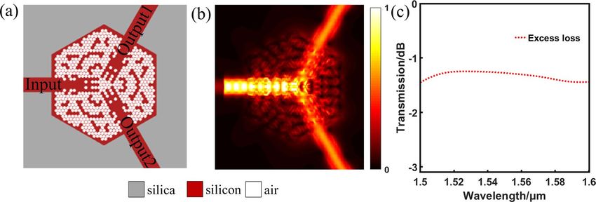
www.nature.com/scientificreports/
Figure 1. The different pixel arrangements. (a) The simple way to arrange pixels. (b) The way to arrange the
pixels of the next row in the gap between the adjacent pixels of the previous row.
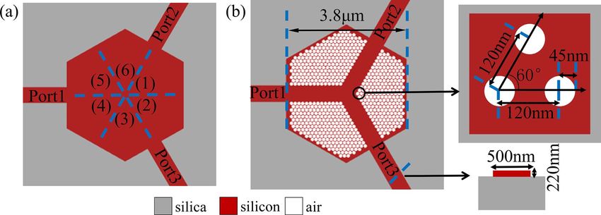
Figure 2. The design of coupling region of arbitrary-input 1 × 2 power splitter. (a) The six symmetric parts of
coupling region. (b) The initial pattern.
devices31,43. In this work, we use DBS algorithm to complete the arbitrary-input 1 × 2 and 1 × 3 power splitters
based on high symmetry, the structure shapes of which are 3.8 μm-wide regular hexagon and 4.0 μm-wide
regular octagon, respectively. Moreover, the excess loss (EL) of the 1 × 2 power splitter is less than 1.5 dB from
1,500 to 1,600 nm. The 1 × 3 power splitter exhibits the EL of less than 1.9 dB and crosstalk (CT) of lower than
− 15.5 dB over 100 nm bandwidth at the centered wavelength of 1,550 nm. We believe the arbitrary-input and
ultra-compact 1 × N power splitters will be highly applied in the PIC and further increase the transmission
capacity of optical communication system.
Methods and results
We use DBS algorithm to simulate and compute the structure of our devices on a SOI platform with 220 nm-thick
top silicon layer. As shown in Fig. 1a, a simple way was widely adopted to arrange pixels. The grey part means
silica layer, the red part stands for silicon layer and the white parts represent the air holes. However, we often get
unexpected results by applying this method to our device, because this pixel combination can not realize high
symmetry. Therefore, our first priority is to find a proper way to arrange the pixels. In the Fig. 1b, we arrange
the pixels of the next row in the gap between the adjacent pixels of the previous row. By this way, we can get the
symmetric and well-distributed pixels in the coupling region.
Being arbitrary-input needs highly symmetric structure. We choose a regular hexagon as the shape of cou-
pling region of 1 × 2 power splitter. As shown in Fig. 2a, the coupling region is divided into six parts and each
part is axisymmetric. If we get the pixel distribution of any part, the distributions of other parts can be obtained
through symmetry. The benefit of this approach is that we can not only get the functionality we want, but also
save a lot of computing time. Since the DBS algorithm is very sensitive to the initial structure, we need to set a
reasonable one in Fig. 2b9,18,30. Here the widths of regular-hexagon design region and every waveguide are 3.8 μm
and 500 nm respectively. In addition, the distance of each circular void is set to 120 nm. The radius and depth
are set to 45 nm and 220 nm, respectively.
The DBS optimization algorithm aims to figure out the optimal void combination. The pixel has two states:
silicon and air. We switch the pixel states of the six axisymmetric parts and calculate the figure of merit (FOM).
Scientific Reports | (2020) 10:11757 | https://doi.org/10.1038/s41598-020-68746-0 2
Vol:.(1234567890)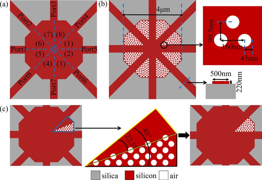
www.nature.com/scientificreports/
Figure 3. The simulated results of arbitrary-input 1 × 2 power splitter. (a) The optimized structure. (b) The
corresponding the distribution of optical field. (c) The simulated spectra transmission of this device.
Power uniformity which is defined as the ratio of the maximum and minimum output powers, is important and
critical aspects for a s plitter29. Since the symmetry of pixel combination is kept during the following optimiza-
tion process so that the imbalance of output ports is negligible. That is to say the transmittances of this device
in the output ports are always uniform. Thus FOM does not need to adjust the imbalance of output ports. FOM
is defined as:
FOM = 1 − (|t1 min − 0.5| + |t2 min − 0.5|) − |t1 min − t2 min | (1)
where t1min and t2min stand for the minimum transmittances of the output ports during all wavelengths, respec-
tively, because we can improve the overall transmittances by only controlling the minimum transmittance9. If the
value of the FOM increases, it means the performance of the device is developed and the state of this pixel should
be maintained. Otherwise, the performance is not optimized and the pixel return to the previous state. Every
time the state of a pixel is toggled, we make a calculation and comparison. When all the pixel states are toggled,
one iteration ends. The device exhibits nice and stable performance when the FOM is not further improved.
Because the three parts, separated by the three waveguides in Fig. 3a, are identical and symmetric, this device
can exhibit the same effect of 1 × 2 power splitting, no matter which waveguide the light field is injected from. We
make further optimization by utilizing 3D fine difference time domain (3D FDTD) solutions. The transmission
efficiencies of output ports, described in Fig. 3b, are uniform. The simulated spectra transmission of this device
is shown in Fig. 3c. Here, the EL is defined as:
tm
ELm = 10 × log (2)
T
where t denotes the transmission efficiency of output port, and the T corresponds to the transmittance of the
input port. Besides m represents the number of output ports. Thus, the EL of this device is less than 1.5 dB from
1,500 to 1,600 nm.
We have explained the design process of an arbitrary-input 1 × 2 power splitter in detail above. In principle,
we can design the arbitrary-input power splitter with any number of waveguide channels. Here we continue to
state an arbitrary-input 1 × 3 power splitter. Considering on the one hand the number of waveguide ports, and
on the other hand the angle between adjacent ports, we design the shape of coupling region as a regular octagon.
It is divided into eight parts and each part is axisymmetric in Fig. 4a. As is shown in Fig. 4b, the initial pattern
is given. Here the width of design region is 4 μm, row spacing of pixel matrix is 99.5 nm, and column spacing of
pixel matrix is 160 nm. Similarly, the radius and depth of air void are 45 nm and 220 nm, respectively. The same
challenge is how to arrange pixels. Firstly, in Fig. 4c, we divide one of eight parts, in the blue box of left picture,
into two symmetric parts, shown by the yellow and black boxes in the middle picture. Secondly, we arrange the
pixels in one part, and then we use symmetry to get the pixel combination of the other. Here we get the pixel
combination of one of the eight parts in right picture of Fig. 4c. At last, once again, we use symmetry to get the
pixel distributions of other parts in Fig. 4a. This method of pixel combination detailed i n21 can not only get as
many pixels as possible, but also make the pixels arrange along the direction of waveguide so as to profit the
propagation of light.
We adopt DBS algorithm to optimize 1 × 3 power splitter as well. Unlike the 1 × 2 power splitter, the transmit-
tance of each port can not always keep uniform during optimization process by symmetry. That is to say, there
needs to be a term in the FOM function to adjust the power uniformity. So root-mean-square error (RMSE)
is employed, which is universally applied to describe the dispersion degree of distribution. It is expressed as:
1/2
1/2
1/2
(t1 − t2 )2 (t1 − t3 )2 (t2 − t3 )2
M= + + (3)
n n n
Scientific Reports | (2020) 10:11757 | https://doi.org/10.1038/s41598-020-68746-0 3
Vol.:(0123456789)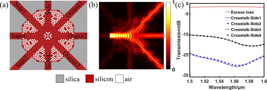
www.nature.com/scientificreports/

                                      Figure 4.  The design of coupling region of arbitrary-input 1 × 3 power splitter. (a) The eight symmetric parts of
                                      coupling region. (b) The initial pattern. (c) The design process of initial pattern.

                                      where t1, t2 and t3 present the transmittances of three output waveguides and n indicates the number of measured
                                      wavelength. This way by utilizing RMSE assures the power uniformity of each port. At the same time, we use N
                                      to indicate the transmittance function, which is defined as:
                                                     N = (t1 min + t2 min + t3 min ) − (|t1 min − t2 min | + |t1 min − t3 min | + |t2 min − t3 min |)     (4)
                                      here t1min, t2min and t3min stand for the minimum transmittances of the three output ports during all wavelengths.
                                      The N is similar to the FOM of 1 × 2 power splitter. It is the task of the inverse algorithm to obtain the high and
                                      uniform transmittances. First and foremost, in order to guarantee high light strength, we want the value of N
                                      to be as big as possible. Furthermore, we need the value of M to be minimal, and preferably close to zero so as
                                      to ensure the uniformity of transmittances. Last but not least, we give the FOM by combining two functions,
                                      which is expressed as:
                                             FOM = α × (t1 min + t2 min + t3 min ) − β × (|t1 min − t2 min | + |t1 min − t3 min | + |t2 min − t3 min |)
                                                                          1/                    1/                     1/
                                                               (t1 − t2 )2 2          (t1 − t3 )2 2           (t2 − t3 )2 2                               (5)

                                                  −γ ×                        +                      +
                                                                  n                      n                       n
                                      we introduce α, β and γ in this formula to balance the weights of M and N. Here they are set to 0.8, 0.1 and 0.1,
                                      respectively. The 3D FDTD simulation is used to make further optimization. It is not hard to notice the truth,
                                      mirrored by Fig. 5a, that the top and bottom of the structure are symmetric about horizontal waveguide, and
                                      the left and right are symmetric with respect to vertical waveguide. Through this design, this device can always
                                      achieve 1 × 3 power splitting in the corresponding output waveguides when the light field is launched from the
                                      top or bottom or left or right waveguide. Figure 5b displays the distribution of light field. The simulated spectra
                                      transmission of this device is shown in Fig. 5c. Here, the CT is expressed as:

                                                                                                       t
                                                                                    CT = 10 × log                                                     (6)
                                                                                                      T
                                      where t denotes the transmission efficiency of side port, and the T corresponds to the transmittance of the
                                      input port. Therefore, this device exhibits the EL of less than 1.9 dB and CT of lower than − 15.5 dB in the broad
                                      bandwidth of 1 µm, respectively.
                                          Generous rewards are accompanied with significant risks. Our devices occupy typical and novel character-
                                      istics, but the transmittances of our device are not as efficient as them without arbitrary-input power splitting.
                                      That is because highly symmetric structure unavoidably curbs the flexibility of pixels search and control ability

          Scientific Reports |   (2020) 10:11757 |                  https://doi.org/10.1038/s41598-020-68746-0                                             4

Vol:.(1234567890)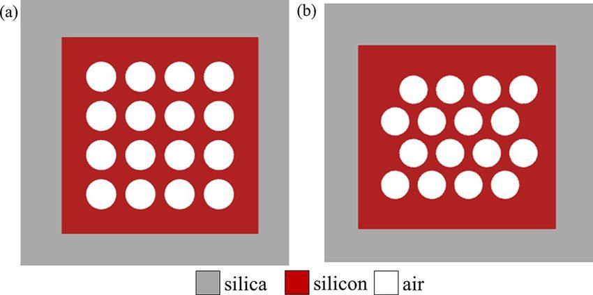
www.nature.com/scientificreports/
Figure 5. The simulated results of arbitrary-input 1 × 3 power splitter. (a) The optimized structure. (b) The
corresponding the distribution of optical field. (c) The simulated spectra transmission of this device.
Figure 6. The simulated spectral responses under the diameter variations from − 10 to 10 nm. (a) The arbitrary-
input 1 × 2 power splitter. (b)–(d) The arbitrary-input 1 × 3 power splitter.
of pixel combination. It inevitably restricts the performance of our device. However, they still pave the way for
the development of PICs.
Tolerance to fabrication errors
The fabrication tolerance must be considered because of the unavoidable and random fabrication imperfection
in practice. Here we simulate the device performances and plot the transmission curves under diameter vari-
ations from − 10 to 10 nm in Fig. 6. Unfortunately, in Fig. 6a the hole size variations have dramatic impact on
the ELs of 1 × 2 power splitter. In the blue curve of Fig. 6a, the 1 × 2 power splitter exhibits the EL of less than
10.2 dB which is an unacceptable result. The loss of each port of 1 × 2 power splitter is always uniform thanks to
the symmetric design of structure. In terms of 1 × 3 power splitter, although the EL and CT curves of 1 × 3 power
splitter in Fig. 6b,c, show slightly fluctuations, the loss of each port becomes greatly nonuniform after imposing
variations of − 10 and 10 nm to the air hole diameters in Fig. 6d, especially in the blue curves. We may reach the
conclusion that smaller hole size greatly affects the performances of these devices, and we may get unexpected
performance under large-scale diameter variations from − 10 to 10 nm.
As the fabrication of nanophotonic components is quite developed, the circular air void without sharp corners
is easy enough to implement in a small-scale diameter variation during f abrication8,30. Thus we can discuss the
fabrication tolerances under slight diameter variations. As is shown in Fig. 7, the simulated spectral responses
under the diameter variations from − 3 to 3 nm are given. Except that there is a significant drop at short wave-
lengths in blue curve of Fig. 7a, the transmission curves of 1 × 2 power splitter on the whole are slightly degraded.
The efficiency drops of ELs are all within 1.5 dB according to the simulated results. In Fig. 7b,c, the hole size
variations have little impact on the ELs and CTs of 1 × 3 power splitter. The fluctuations of ELs are only within
0.5 dB, and the CTs are still lower than − 14.9 dB. In addition, the loss of each port of 1 × 3 power splitter is very
uniform in Fig. 7d. This suggests an acceptable fabrication tolerance of the designed devices.
Conclusion
In the paper, we make full use of the symmetric structure to design and theoretically simulate arbitrary-input
and ultra-compact power splitters. In principle, we can design any number of waveguide channels. Here we
mainly propose 1 × 2 and 1 × 3 power splitter. The excess loss of the 1 × 2 power splitter is less than 1.5 dB from
1,500 to 1,600 nm, and the excess loss and crosstalk of the 1 × 3 power splitter are less than 1.9 dB and lower
than − 15.5 dB over 100 nm bandwidth at the centered wavelength of 1,550 nm. The tolerances to fabrication
errors are also investigated. The best advantage of our work is that these devices can achieve power splitting, no
Scientific Reports | (2020) 10:11757 | https://doi.org/10.1038/s41598-020-68746-0 5
Vol.:(0123456789)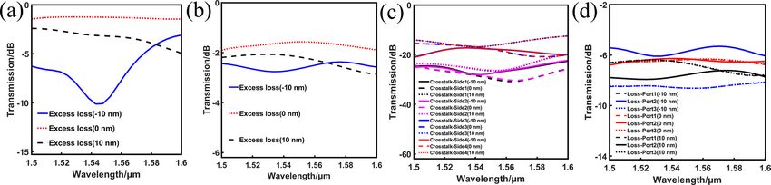
www.nature.com/scientificreports/
Figure 7. The simulated spectral responses under the diameter variations from − 3 to 3 nm. (a) The arbitrary-
input 1 × 2 power splitter. (b)–(d) The arbitrary-input 1 × 3 power splitter.
matter which port the light field is launched from. Although we have only achieved a little, we provide a kind of
new approach to enhance the transmission capacity of on-chip optical interconnect.
Received: 10 March 2020; Accepted: 26 June 2020
References
1. Ding, Y. et al. On-chip two-mode division multiplexing using tapered directional coupler-based mode multiplexer and demulti-
plexer. Opt. Express 21, 10376–10382 (2013).
2. Chang, W. et al. Ultra-compact mode (de) multiplexer based on subwavelength asymmetric Y-junction. Opt. Express 26, 8162–8170
(2018).
3. Luo, L. W. et al. WDM-compatible mode-division multiplexing on a silicon chip. Nat. Commun. 5, 1–7 (2014).
4. Liu, Y. et al. Arbitrarily routed mode-division multiplexed photonic circuits for dense integration. Nat. Commun. 10, 1–7 (2019).
5. Liu, Y. et al. Very sharp adiabatic bends based on an inverse design. Opt. Lett. 43, 2482–2485 (2018).
6. Tahersima, M. H. et al. Deep neural network inverse design of integrated photonic power splitters. Sci. Rep. 9, 1–9 (2019).
7. Sakamaki, Y. et al. Y-branch waveguides with stabilized splitting ratio designed by wavefront matching method. IEEE Photonics
Technol. Lett. 18, 817–819 (2006).
8. Lu, L. et al. Inverse-designed single-step-etched colorless 3 dB couplers based on RIE-lag-insensitive PhC-like subwavelength
structures. Opt. Lett. 41, 5051–5054 (2016).
9. Ma, H., Huang, J., Zhang, K. & Yang, J. Arbitrary-direction, multichannel and ultra-compact power splitters by inverse design
method. Opt. Commun. 462, 125329 (2020).
10. Zhang, Y. et al. A compact and low loss Y-junction for submicron silicon waveguide. Opt. Express 21, 1310–1316 (2013).
11. Zhang, Y. et al. High-extinction-ratio silicon polarization beam splitter with tolerance to waveguide width and coupling length
variations. Opt. Express 24, 6586–6593 (2016).
12. Lou, F., Dai, D. & Wosinski, L. Ultracompact polarization beam splitter based on a dielectric–hybrid plasmonic–dielectric coupler.
Opt. Lett. 37, 3372–3374 (2012).
13. Shen, B., Wang, P., Polson, R. & Menon, R. An integrated-nanophotonics polarization beamsplitter with 2.4× 2.4 μm2 footprint.
Nat. Photonics 9, 378–382 (2015).
14. Dai, D. & Bowers, J. E. Novel ultra-short and ultra-broadband polarization beam splitter based on a bent directional coupler. Opt.
Express 19, 18614–18620 (2011).
15. Liu, Y. et al. Subwavelength polarization splitter–rotator with ultra-compact footprint. Opt. Lett. 44, 4495–4498 (2019).
16. Majumder, A., Helms, P. L., Andrew, T. L. & Menon, R. A comprehensive simulation model of the performance of photochromic
films in absorbance-modulation-optical-lithography. AIP Adv. 6, 035210 (2016).
17. Majumder, A. et al. Reverse-absorbance-modulation-optical lithography for optical nanopatterning at low light levels. AIP Adv.
6, 065312 (2016).
18. Majumder, A., Shen, B., Polson, R., Andrew, T., & Menon, R. An ultra-compact nanophotonic optical modulator using multi-state
topological optimization. Preprint at https://arxiv.xilesou.top/abs/1712.02835 (2017).
19. Chang, W. et al. An ultracompact multimode waveguide crossing based on subwavelength asymmetric Y-junction. IEEE Photonics
J. 10, 1–8 (2018).
20. Bogaerts, W., Dumon, P., Van Thourhout, D. & Baets, R. Low-loss, low-cross-talk crossings for silicon-on-insulator nanophotonic
waveguides. Opt. Lett. 32, 2801–2803 (2007).
21. Lu, L. et al. Inverse-designed ultra-compact star-crossings based on PhC-like subwavelength structures for optical intercross con-
nect. Opt. Express 25, 18355–18364 (2017).
22. Li, Y. et al. Hybrid plasmonic waveguide crossing based on the multimode interference effect. Opt. Commun. 335, 86–89 (2015).
23. Chen, H. & Poon, A. W. Low-loss multimode-interference-based crossings for silicon wire waveguides. IEEE Photonics Technol.
Lett. 18(21), 2260–2262 (2006).
24. Dai, D., Wang, J. & Shi, Y. Silicon mode (de)multiplexer enabling high capacity photonic networks-on-chip with a single-wave-
length-carrier light. Opt. Lett. 38, 1422–1424 (2013).
25. Wang, J., He, S. & Dai, D. On-chip silicon 8-channel hybrid (de) multiplexer enabling simultaneous mode-and polarization-
division-multiplexing. Laser. Photonics Rev. 8, L18–L22 (2014).
26. Frellsen, L. F., Ding, Y., Sigmund, O. & Frandsen, L. H. Topology optimized mode multiplexing in silicon-on-insulator photonic
wire waveguides. Opt. Express 24, 16866–16873 (2016).
27. Xie, H. et al. Highly compact and efficient four-mode multiplexer based on pixelated waveguides. IEEE Photonics Technol. Lett.
32, 166–169 (2020).
28. Gamet, J. & Pandraud, G. Ultralow-loss 1 × 8 splitter based on field matching Y junction. IEEE Photonics Technol. Lett. 16,
2060–2062 (2004).
29. Tao, S. H. et al. Cascade wide-angle y-junction 1 × 16 optical power splitter based on silicon wire waveguides on silicon-on-
insulator. Opt. Express 16, 21456–21461 (2008).
30. Lu, L., Zhang, M., Zhou, F. & Liu, D. An ultra-compact colorless 50: 50 coupler based on PhC-like metamaterial structure. In
Optical Fiber Communications Conference and Exhibition. IEEE 1–3 (2016).
Scientific Reports | (2020) 10:11757 | https://doi.org/10.1038/s41598-020-68746-0 6
Vol:.(1234567890)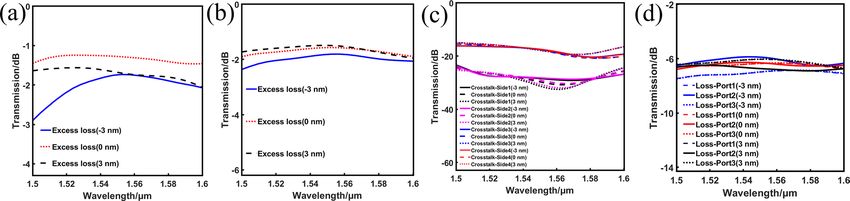
www.nature.com/scientificreports/
31. Piggott, A. Y. Automated design of photonic devices. https : //a.glgoo . top/books ? hl=zh-CN&lr=&id=habQD w AAQB
AJ&oi=fnd&pg=PR4&dq=Automated+design+of+photonic+devices&ots=eLJKn0HT6B&sig=36rki3cEHNU9t9IlnIVcO8rnF
RQ#v=onepage&q=Automated%2520design%2520of%2520photonic%2520devices&f=false (Alexander Yukio Piggott 2018).
32. Xu, K. et al. Integrated photonic power divider with arbitrary power ratios. Opt. Lett. 42, 855–858 (2017).
33. Xie, H. et al. Inversely designed 1 × 4 power splitter with arbitrary ratios at 2-μm spectral band. IEEE Photonics J. 10, 1 (2018).
34. Chang, W., Lu, L., Liu, D., & Zhang, M. An ultra-compact colorless dual-mode 3 dB power splitter based on axisymmetrical
subwavelength structure. In CLEO: Science and Innovations (Optical Society of America, JW2A-47, 2018).
35. Xie, H. et al. An ultra-compact 3-dB power splitter for three modes based on pixelated meta-structure. IEEE Photonics Technol.
Lett. 32, 341–344 (2020).
36. Ma, H., Huang, J., Zhang, K. & Yang, J. Ultra-compact and efficient 1 × 2 mode converters based on rotatable direct-binary-search
algorithm. Opt. Express 11, 17010–17019 (2020).
37. Liu, Z. et al. Integrated nanophotonic wavelength router based on an intelligent algorithm. Optica 6, 1367–1373 (2019).
38. Li, Z., Zhang, Z., Huang, J. & Yang, J. Genetically designed ultra-compact wideband multiple-use reflectors with high reflectivity
applying to optics communication. In IEEE 19th International Conference on Communication Technology (ICCT) 724–728 (2019).
39. Huang, J. et al. Implementation of on-chip multi-channel focusing wavelength demultiplexer with regularized digital metamateri-
als. Nanophotonics https://doi.org/10.1515/nanoph-2019-0368 (2019).
40. Huang, J. et al. Ultra-compact broadband polarization beam splitter with strong expansibility. Photonics Res. 6, 574–578 (2018).
41. Lu, J. & Vučković, J. Objective-first design of high-efficiency, small-footprint couplers between arbitrary nanophotonic waveguide
modes. Opt. Express 20, 7221–7236 (2012).
42. Piggott, A. Y., Petykiewicz, J., Su, L. & Vučković, J. Fabrication-constrained nanophotonic inverse design. Sci. Rep. 7, 1–7 (2017).
43. Lu, J. & Vučković, J. Nanophotonic computational design. Opt. Express 21, 13351–13367 (2013).
Acknowledgements
This work is supported by the National Natural Science Foundation of China (60907003, 61805278), the China
Postdoctoral Science Foundation (2018M633704), the Foundation of NUDT (JC13-02-13, ZK17-03-01), the
Hunan Provincial Natural Science Foundation of China (13JJ3001), and the Program for New Century Excellent
Talents in University (NCET-12-0142).
Author contributions
H.M. and J.H. contributed to the idea. H.M. performed the numerical simulation, collected the data and wrote
the manuscript. K.Z. and J.Y. directed the project. All authors discussed the results and revised the manuscript.
Competing interests
The authors declare no competing interests.
Additional information
Correspondence and requests for materials should be addressed to K.Z. or J.Y.
Reprints and permissions information is available at www.nature.com/reprints.
Publisher’s note Springer Nature remains neutral with regard to jurisdictional claims in published maps and
institutional affiliations.
Open Access This article is licensed under a Creative Commons Attribution 4.0 International
License, which permits use, sharing, adaptation, distribution and reproduction in any medium or
format, as long as you give appropriate credit to the original author(s) and the source, provide a link to the
Creative Commons license, and indicate if changes were made. The images or other third party material in this
article are included in the article’s Creative Commons license, unless indicated otherwise in a credit line to the
material. If material is not included in the article’s Creative Commons license and your intended use is not
permitted by statutory regulation or exceeds the permitted use, you will need to obtain permission directly from
the copyright holder. To view a copy of this license, visit http://creativecommons.org/licenses/by/4.0/.
© The Author(s) 2020
Scientific Reports | (2020) 10:11757 | https://doi.org/10.1038/s41598-020-68746-0 7
Vol.:(0123456789)You can also read